
Ion-Driven Electrochemical Random-Access Memory-Based Synaptic Devices for Neuromorphic Computing Systems: A Mini-Review

Abstract
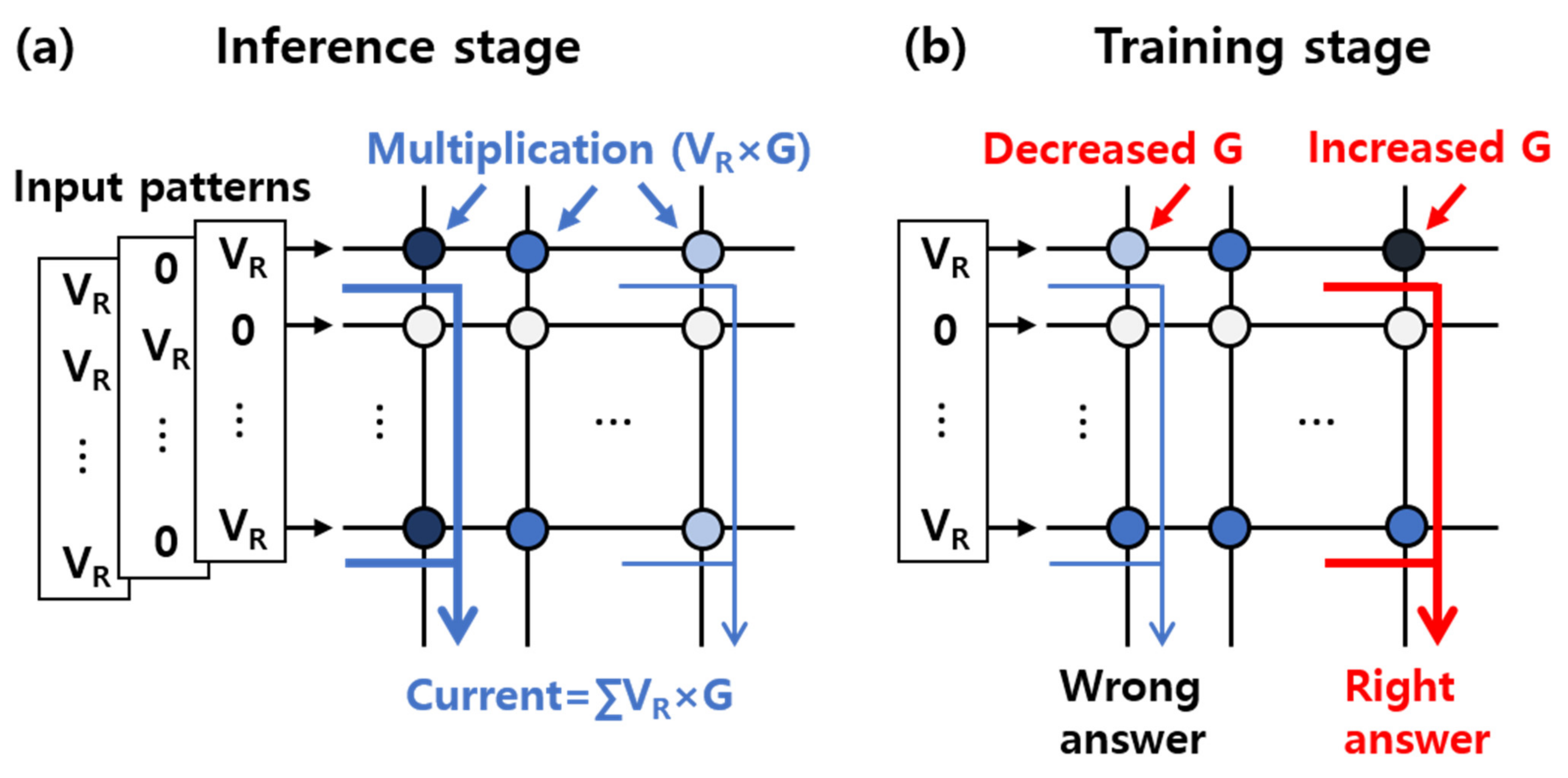
:1. Introduction
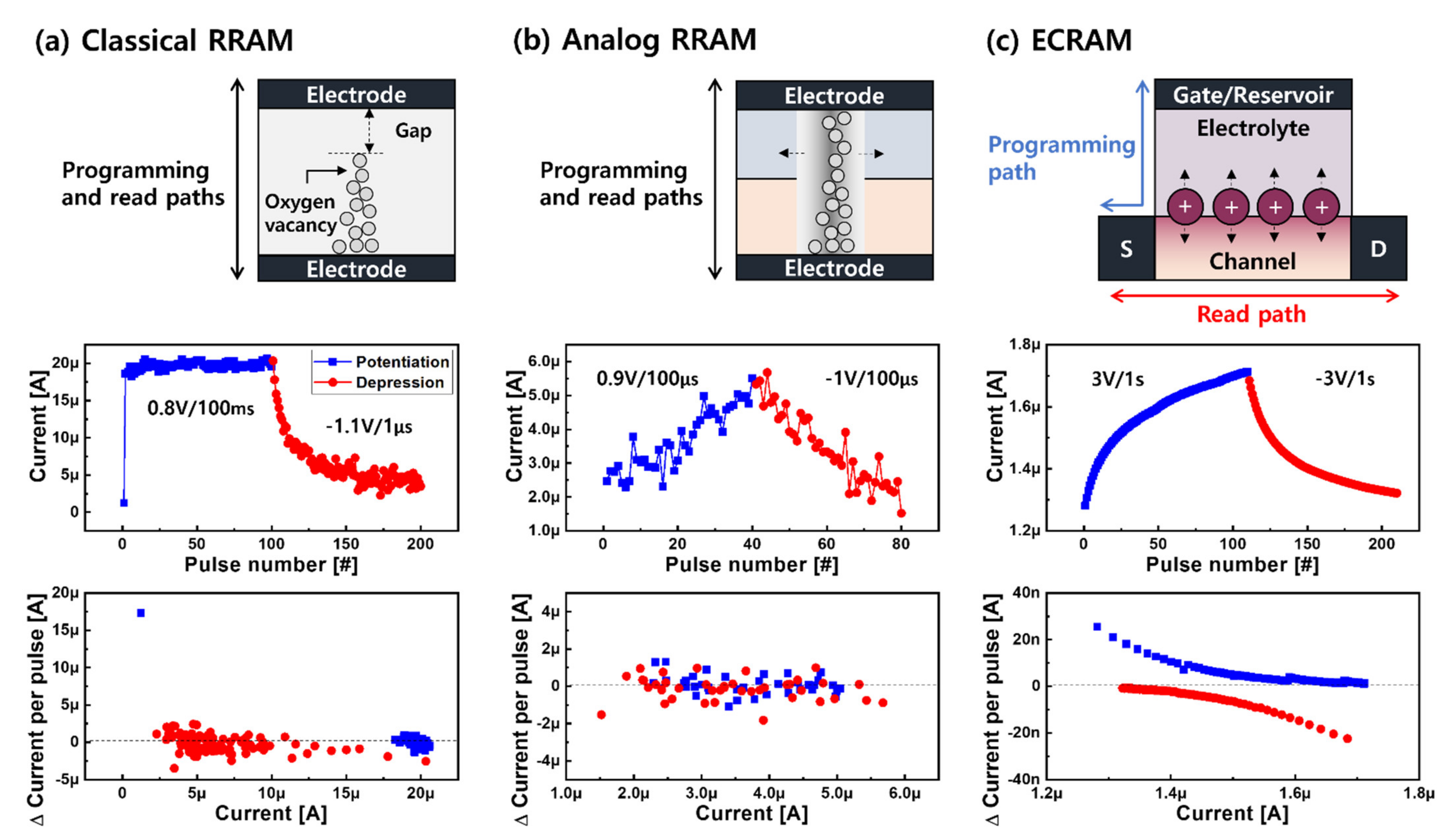
2. Results and Discussion
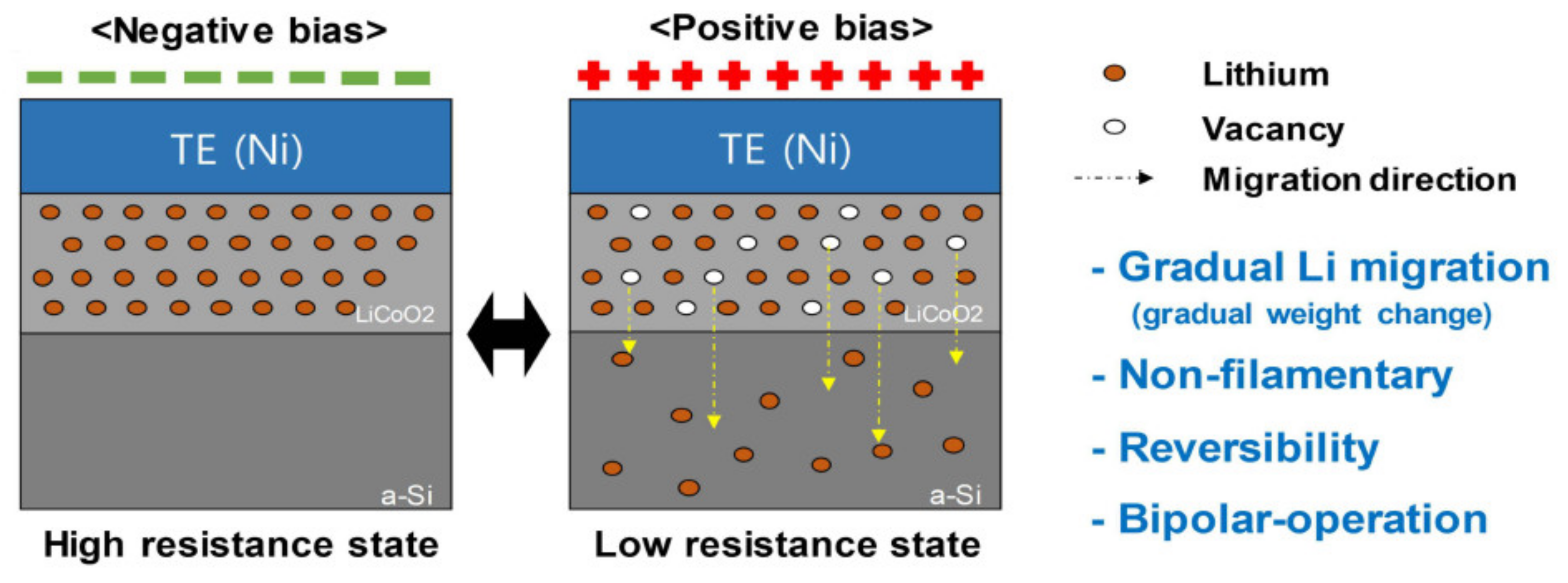
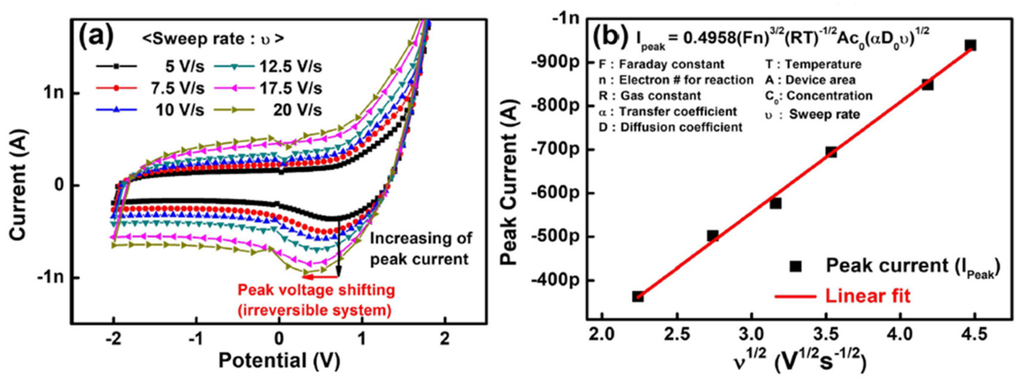
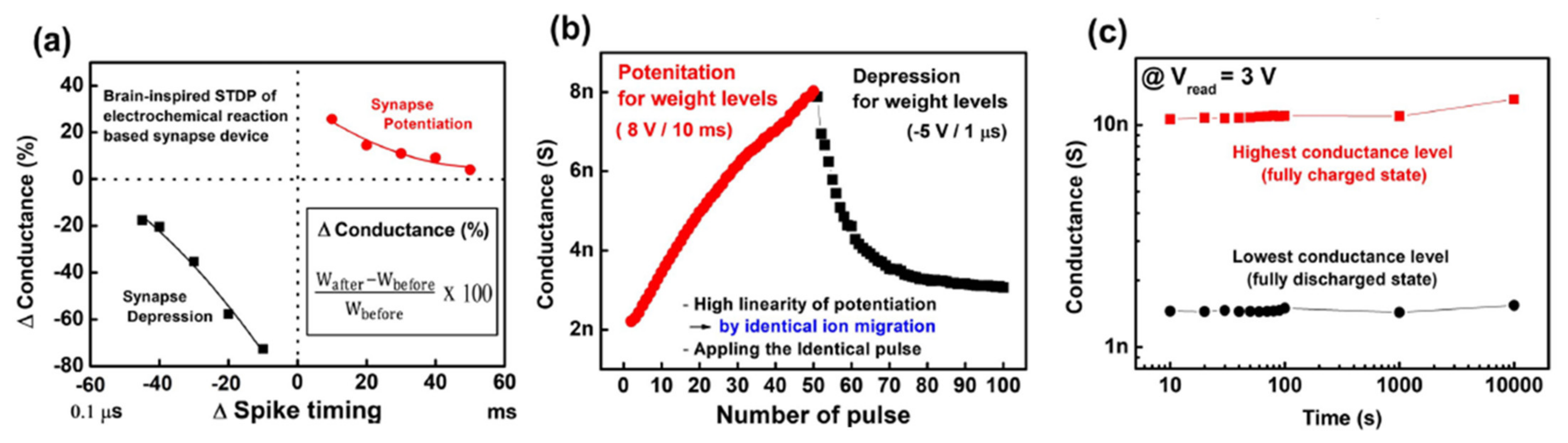
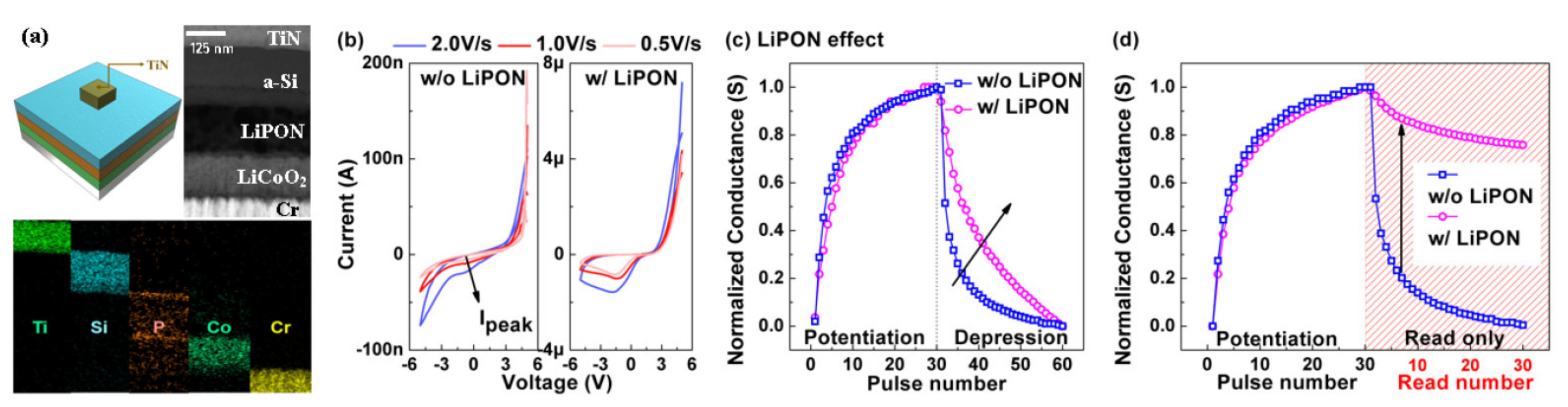
2.1. Li-Ion-Based Electrochemical Random-Access Memory
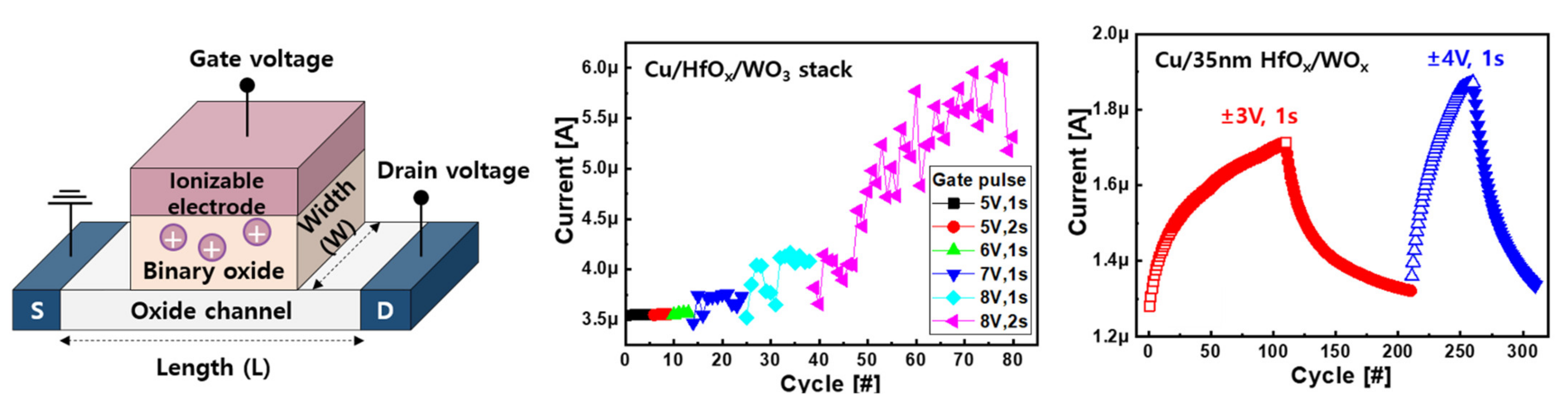
2.2. Oxygen-Ion-Based Electrochemical Random-Access Memory

| Device stack | Electrolyte | Ionic Liquid | HfO2 | HfO2 | HfO1.74 | HfOx | YSZ |
|---|---|---|---|---|---|---|---|
| Channel | SmNiO3 | WO3 | WOX | PCMO | PCMO | TiOx | |
| Mobile ion | Oxygen ion | Oxygen ion | Oxygen ion | Oxygen ion | Oxygen ion | Oxygen ion | |
| Conductance range | 1.1 | 20 | ~6 | ~1.75 | ~2.25 | 7 | |
| Driving conditions | Potentiation | −2.5 V/10 ms | +1 nA/0.5 s | +4 V/1 s | −3.75 V/1 s | −3.5 V/100 ms | +4 V/500 ms |
| Depression | +2.5 V/10 ms | −1 nA/0.5 s | −3 V/1 s | 3V/1 s | 2.5 V/100 ms | −3.5 V/500 ms | |
| Reference | [22] | [18] | [29] | [26] | [27] | [28] | |
2.3. Proton-Based Electrochemical Random-Access Memory
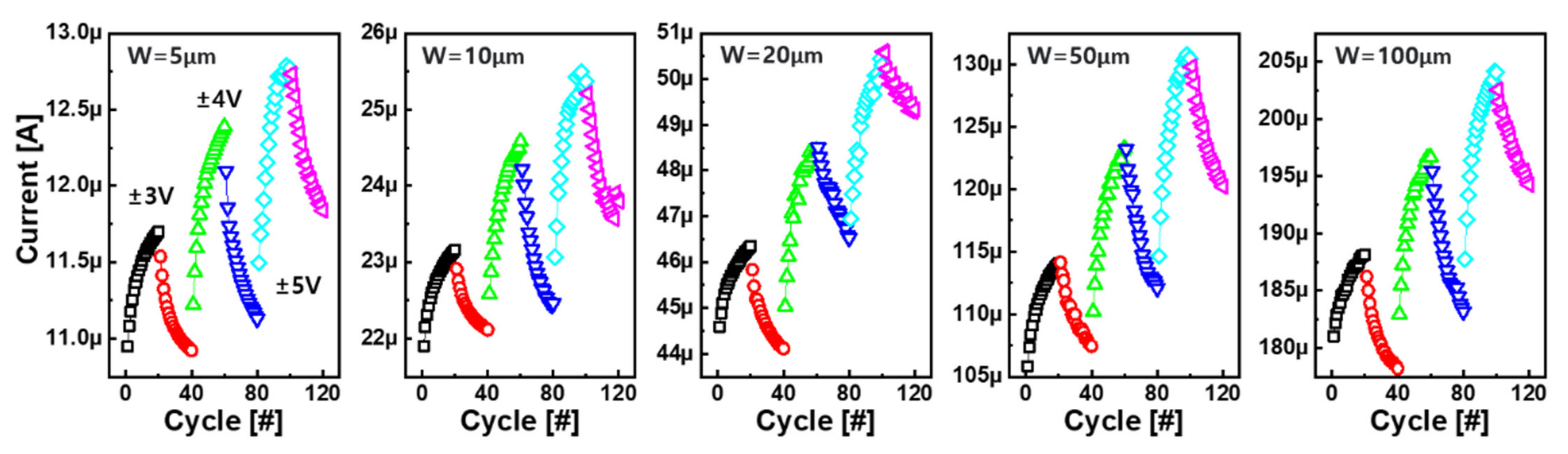
2.4. Cu-Ion-Based Electrochemical Random-Access Memory
3. Conclusions
Author Contributions
Funding
Data Availability Statement
Conflicts of Interest
References
- Mead, C. Neuromorphic electronic systems. Proc. IEEE 1990, 78, 1629–1636. [Google Scholar] [CrossRef] [Green Version]
- Burr, G.W.; Shelby, R.M.; Sebastian, A.; Kim, S.; Kim, S.; Sidler, S.; Virwani, K.; Ishii, M.; Narayanan, P.; Fumarola, A.; et al. Neuromorphic computing using non-volatile memory. Adv. Phys. X 2017, 2, 89–124. [Google Scholar] [CrossRef]
- Zhang, Y.; Wang, Z.; Zhu, J.; Yang, Y.; Rao, M.; Song, W.; Zhuo, Y.; Zhang, X.; Cui, M.; Shen, L.; et al. Brain-inspired computing with memristors: Challenges in devices, circuits, and systems. Appl. Phys. Rev. 2019, 7, 011308. [Google Scholar] [CrossRef]
- Wan, Q.; Shi, Y. Neuromorphic Devices for Brain-Inspired Computing: Artificial Intelligence, Perception and Robotics, 1st ed.; Wiley-VCH: Weinheim, Germany, 2022. [Google Scholar]
- Song, Y.J.; Lee, J.H.; Han, S.H.; Shin, H.C.; Lee, K.H.; Suh, K.; Jeong, D.E.; Koh, G.H.; Oh, S.C.; Park, J.H.; et al. Demonstration of Highly Manufacturable STT-MRAM Embedded in 28nm Logic. In Proceedings of the IEEE International Electron Devices Meeting (IEDM), San Francisco, CA, USA, 1–5 December 2018; p. 182. [Google Scholar]
- Jackson, B.L.; Rajendran, B.; Corrado, G.S.; Breitwisch, M.; Burr, G.W.; Cheek, R.; Gopalakrishnan, K.; Raoux, S.; Rettner, C.T.; Padilla, A.; et al. Nanoscale Electronic Synapses Using Phase Change Devices. ACM J. Emerg. Technol. Comput. Syst. 2013, 9, 12. [Google Scholar] [CrossRef]
- Horii, H.; Yi, J.; Park, J.; Ha, Y.; Baek, I.; Park, S.; Hwang, Y.; Lee, S.; Kim, Y.; Lee, K.; et al. A novel cell technology using N-doped GeSbTe films for phase change RAM. In Proceedings of the 2003 Symposium on VLSI Technology, Kyoto, Japan, 10–12 June 2003. [Google Scholar] [CrossRef]
- Yao, P.; Wu, H.; Gao, B.; Tang, J.; Zhang, Q.; Zhang, W.; Yang, J.J.; Qian, H. Fully hardware-implemented memristor convolu-tional neural network. Nature 2020, 577, 641–646. [Google Scholar] [CrossRef]
- Li, C.; Hu, M.; Li, Y.; Jiang, H.; Ge, N.; Montgomery, E.; Zhang, J.; Song, W.; Dávila, N.; Graves, C.; et al. Analogue signal and image processing with large memristor crossbars. Nat. Electron. 2017, 1, 52–59. [Google Scholar] [CrossRef]
- Woo, J.; Yu, S. Resistive Memory-Based Analog Synapse: The Pursuit for Linear and Symmetric Weight Update. IEEE Nanotechnol. Mag. 2018, 12, 36–44. [Google Scholar] [CrossRef]
- Yu, S.; Chen, P.-Y.; Cao, Y.; Xia, L.; Wang, Y.; Wu, H. Scaling-up Resistive Synaptic Arrays for Neuro-inspired Architecture: Challenges and Prospect. In Proceedings of the IEEE International Electron Devices Meeting (IEDM), Washington, DC, USA, 7–9 December 2015; p. 17.3. [Google Scholar]
- Woo, J.; Moon, K.; Song, J.; Lee, S.; Kwak, M.; Park, J.; Hwang, H. Improved Synaptic Behavior Under Identical Pulses Using AlOx/HfO2 Bilayer RRAM Array for Neuromorphic Systems. IEEE Electron Device Lett. 2016, 37, 994–997. [Google Scholar] [CrossRef]
- Woo, J.; Padovani, A.; Moon, K.; Kwak, M.; Larcher, L.; Hwang, H. Linking Conductive Filament Properties and Evolution to Synaptic Behavior of RRAM Devices for Neuromorphic Applications. IEEE Electron Device Lett. 2017, 38, 1220–1223. [Google Scholar] [CrossRef]
- Wu, W.; Wu, H.; Gao, B.; Deng, N.; Yu, S.; Qian, H. Improving Analog Switching in HfOx-Based Resistive Memory with a Thermal Enhanced Layer. IEEE Electron Device Lett. 2017, 38, 1019–1022. [Google Scholar] [CrossRef]
- Fuller, E.J.; El Gabaly, F.; Léonard, F.; Agarwal, S.; Plimpton, S.J.; Jacobs-Gedrim, R.B.; James, C.D.; Marinella, M.J.; Talin, A.A. Li-Ion Synaptic Transistor for Low Power Analog Computing. Adv. Mater. 2016, 29. [Google Scholar] [CrossRef] [PubMed]
- Tang, J.; Bishop, D.; Kim, S.; Copel, M.; Gokmen, T.; Todorov, T.; Shin, S.H.; Lee, K.-T.; Solomon, P.; Chan, K.; et al. ECRAM as Scalable Synaptic Cell for High-Speed, Low-Power Neuromorphic Computing. In Proceedings of the IEEE International Electron Devices Meeting (IEDM), San Francisco, CA, USA, 1–5 December 2018; p. 13.1. [Google Scholar]
- Hasegawa, T.; Itoh, Y.; Tanaka, H.; Hino, T.; Tsuruoka, T.; Terabe, K.; Miyazaki, H.; Tsukagoshi, K.; Ogawa, T.; Yamaguchi, S.; et al. Volatile/Nonvolatile Dual-Functional Atom Transistor. Appl. Phys. Express 2010, 4, 015204. [Google Scholar] [CrossRef]
- Kim, S.; Todorov, T.; Onen, M.; Gokmen, T.; Bishop, D.; Solomon, P.; Lee, K.-T.; Copel, M.; Farmer, D.B.; Ott, J.A.; et al. Metal-oxide based, CMOS-compatible ECRAM for Deep Learning Accelerator. In Proceedings of the IEEE International Electron Devices Meeting (IEDM), San Francisco, CA, USA, 7–11 December 2019; p. 35.7.1. [Google Scholar]
- Kang, H.; Woo, J. Cu-ion-actuated three-terminal neuromorphic synaptic devices based on binary metal-oxide electrolyte and channel. Appl. Phys. Lett. 2021, 119, 072103. [Google Scholar] [CrossRef]
- Lee, C.; Lee, J.; Kim, M.; Woo, J.; Koo, S.-M.; Oh, J.-M.; Lee, D. Two-terminal structured synaptic device using ionic elec-trochemical reaction mechanism for neuromorphic system. IEEE Electron Device Lett. 2019, 40, 546–549. [Google Scholar] [CrossRef]
- Choi, Y.; Lee, C.; Kim, M.; Song, Y.; Hwang, H.; Lee, D. Structural Engineering of Li-Based Electronic Synapse for High Reliability. IEEE Electron Device Lett. 2019, 40, 1992–1995. [Google Scholar] [CrossRef]
- Shi, J.; Ha, S.D.; Zhou, Y.; Schoofs, F.; Ramanathan, S. A correlated nickelate synaptic transistor. Nat. Commun. 2013, 4, 2676. [Google Scholar] [CrossRef] [Green Version]
- Sawa, A. Resistive switching in transition metal oxides. Mater. Today 2008, 11, 28–36. [Google Scholar] [CrossRef]
- Siddik, M.; Jung, S.; Park, J.; Lee, W.; Kim, S.; Lee, J.; Shin, J.; Park, S.; Lee, D.; Kim, I.; et al. Thermally assisted resistive switching in Pr0.7Ca0.3MnO3/Ti/Ge2Sb2Te5 stack for nonvolatile memory applications. Appl. Phys. Lett. 2011, 99, 063501. [Google Scholar] [CrossRef]
- Baek, K.; Park, S.; Park, J.; Kim, Y.-M.; Hwang, H.; Oh, S.H. In situ TEM observation on the interface-type resistive switching by electrochemical redox reactions at a TiN/PCMO interface. Nanoscale 2017, 2, 582–593. [Google Scholar] [CrossRef]
- Lee, C.; Rajput, K.G.; Choi, W.; Kwak, M.; Nikam, R.D.; Kim, S.; Hwang, H. Pr0.7Ca0.3MnO3-Based Three-Terminal Synapse for Neuromorphic Computing. IEEE Electron Device Lett. 2020, 41, 1500–1503. [Google Scholar] [CrossRef]
- Lee, C.; Choi, W.; Kwak, M.; Kim, S.; Hwang, H. Impact of electrolyte density on synaptic characteristics of oxygen-based ionic synaptic transistor. Appl. Phys. Lett. 2021, 119, 103503. [Google Scholar] [CrossRef]
- Lee, J.; Nikam, R.D.; Kwak, M.; Kwak, H.; Kim, S.; Hwang, H. Improvement of Synaptic Properties in Oxygen-Based Synaptic Transistors Due to the Accelerated Ion Migration in Sub-Stoichiometric Channels. Adv. Electron. Mater. 2021, 7, 2100219. [Google Scholar] [CrossRef]
- Jeong, Y.; Lee, H.; Gil Ryu, D.; Cho, S.H.; Lee, G.; Kim, S.; Kim, S.; Lee, Y.S. Elucidating Ionic Programming Dynamics of Metal-Oxide Electrochemical Memory for Neuromorphic Computing. Adv. Electron. Mater. 2021, 7, 2100185. [Google Scholar] [CrossRef]
- Lee, J.; Lim, S.; Kwak, M.; Song, J.; Hwang, H. Understanding of proton induced synaptic behaviors in three-terminal synapse device for neuromorphic systems. Nanotechnology 2019, 30, 255202. [Google Scholar] [CrossRef]
- Van De Burgt, Y.Y.; Lubberman, E.; Fuller, E.J.; Keene, S.; Faria, G.C.; Agarwal, S.; Marinella, M.J.; Talin, A.; Salleo, A. A non-volatile organic electrochemical device as a low-voltage artificial synapse for neuromorphic computing. Nat. Mater. 2017, 16, 414–418. [Google Scholar] [CrossRef]
- Fuller, E.J.; Keene, S.T.; Melianas, A.; Wang, Z.; Agarwal, S.; Li, Y.; Tuchman, Y.; James, C.D.; Marinella, M.J.; Yang, J.J.; et al. Parallel programming of an ionic floating-gate memory array for scalable neuromorphic computing. Science 2019, 364, 570–574. [Google Scholar] [CrossRef]
- Yao, X.; Klyukin, K.; Lu, W.; Onen, M.; Ryu, S.; Kim, D.; Emond, N.; Waluyo, I.; Hunt, A.; Del Alamo, J.A.; et al. Protonic solid-state electrochemical synapse for physical neural networks. Nat. Commun. 2020, 11, 3134. [Google Scholar] [CrossRef]
- Yang, C.S.; Shang, D.S.; Liu, N.; Shi, G.; Shen, X.; Yu, R.C.; Li, Y.Q.; Sun, Y. A Synaptic Transistor based on Quasi-2D Mo-lybdenum Oxide. Adv. Mater. 2017, 29, 1700906. [Google Scholar] [CrossRef]
- Belmonte, A.; Kim, W.; Chan, B.T.; Heylen, N.; Fantini, A.; Houssa, M.; Jurczak, M.; Goux, L. A Thermally Stable and High-Performance 90-nm Al2O3\Cu-Based 1T1R CBRAM Cell. IEEE Trans. Electron Devices 2013, 60, 3690–3695. [Google Scholar] [CrossRef]
- Sills, S.; Yasuda, S.; Strand, J.; Calderoni, A.; Aratani, K.; Johnson, A.; Ramaswamy, N. A copper ReRAM cell for Storage Class Memory applications. In Proceedings of the 2014 Symposium on VLSI Technology (VLSI-Technology), Honolulu, HI, USA, 9–12 June 2014; pp. 1–2. [Google Scholar] [CrossRef]
- Miyamura, M.; Tada, M.; Sakamoto, T.; Banno, N.; Okamoto, K.; Iguchi, N.; Hada, H. First Demonstration of Logic Map-ping on Nonvolatile Programmable Cell Using Complementary Atom Switch. In Proceedings of the IEEE International Electron Devices Meeting (IEDM), San Francisco, CA, USA, 10–13 December 2012; p. 10.6. [Google Scholar]
- Todorov, T.K.; Ando, T.; Narayanan, V.; Rozen, J. Three-Terminal Copper-Driven Neuromorphic Device. U.S. Patent 16/295986, 10 September 2020. [Google Scholar]
- Li, Y.; Fuller, E.J.; Asapu, S.; Agarwal, S.; Kurita, T.; Yang, J.J.; Talin, A.A. Low-Voltage, CMOS-Free Synaptic Memory Based on LiXTiO2 Redox Transistors. ACS Appl. Mater. Interfaces 2019, 11, 38982–38992. [Google Scholar] [CrossRef]
- Nikam, R.D.; Kwak, M.; Lee, J.; Rajput, K.G.; Banerjee, W.; Hwang, H. Near ideal synaptic functionalities in Li ion syn-aptic transistor using Li3POxSex electrolyte with high ionic conductivity. Sci. Rep. 2019, 9, 18883. [Google Scholar] [CrossRef] [PubMed] [Green Version]
- Lee, K.; Lee, J.; Nikam, R.D.; Heo, S.; Hwang, H. Sodium-based nano-ionic synaptic transistor with improved retention characteristics. Nanotechnology 2020, 31, 455204. [Google Scholar] [CrossRef] [PubMed]
- Baldo, M.; Ielmini, D. Modeling of oxide-based ECRAM programming by drift-diffusion ion transport. In Proceedings of the 2021 IEEE International Memory Workshop (IMW), Dresden, Germany, 16–19 May 2021; pp. 1–4. [Google Scholar] [CrossRef]
- Solomon, P.M.; Bishop, D.M.; Todorov, T.K.; Dawes, S.; Farmer, D.B.; Copel, M.; Lee, K.-T.; Collins, J.; Rozen, J. Transient Investigation of Metal-oxide based, CMOS-compatible ECRAM. In Proceedings of the IEEE International Reliability Physics Symposium (IRPS), Monterey, CA, USA, 21–25 March 2021. [Google Scholar]


| Device stack | Electrolyte | Ionic Liquid | PEDOT:PSS | Nafion | SiOx | Nafion |
|---|---|---|---|---|---|---|
| Channel | MoO3 | PEDOT:PSS/PEI | PEDOT:PSS | WO2.7 | WO3 | |
| Mobile ion | Hydrogen | Hydrogen | Hydrogen | Hydrogen | Hydrogen | |
| Conductance range | ~1.35 | ~1.5 | ~2 | ~6 | ~4 | |
| Driving conditions | Potentiation | +2.5 V/1 ms | −100 mV | −1.1 V/50 ms | +3 V/1 s with -1 V/0.5 s | +0.25 V/5 ms |
| Depression | −1.8 V/1 ms | +100 mV | +1 V/50 ms | −2.5 V/1s with +1 V/0.5 s | −0.25 V/5 ms | |
| Reference | [34] | [31] | [32] | [28] | [33] | |
| Device Stack | Cu/Ta2O5 | Cu/Cu6Rb41Cl13/TiN (or TaN) | Cu/HfOx/WOx |
|---|---|---|---|
| Volatility | Nonvolatile | Nonvolatile | Nonvolatile |
| Resistance state | Binary | Analog | Analog |
| Switching mechanism | Forming and dissolution of Cu nucleus | Plating and deplating of Cu | Valence change |
| Applications | Logic | Analog synapse | Analog synapse |
| Reference | [17] | [38] | [19] |
Publisher’s Note: MDPI stays neutral with regard to jurisdictional claims in published maps and institutional affiliations. |
© 2022 by the authors. Licensee MDPI, Basel, Switzerland. This article is an open access article distributed under the terms and conditions of the Creative Commons Attribution (CC BY) license (https://creativecommons.org/licenses/by/4.0/).
Share and Cite
Kang, H.; Seo, J.; Kim, H.; Kim, H.W.; Hong, E.R.; Kim, N.; Lee, D.; Woo, J. Ion-Driven Electrochemical Random-Access Memory-Based Synaptic Devices for Neuromorphic Computing Systems: A Mini-Review. Micromachines 2022, 13, 453. https://doi.org/10.3390/mi13030453
Kang H, Seo J, Kim H, Kim HW, Hong ER, Kim N, Lee D, Woo J. Ion-Driven Electrochemical Random-Access Memory-Based Synaptic Devices for Neuromorphic Computing Systems: A Mini-Review. Micromachines. 2022; 13(3):453. https://doi.org/10.3390/mi13030453
Chicago/Turabian StyleKang, Heebum, Jongseon Seo, Hyejin Kim, Hyun Wook Kim, Eun Ryeong Hong, Nayeon Kim, Daeseok Lee, and Jiyong Woo. 2022. "Ion-Driven Electrochemical Random-Access Memory-Based Synaptic Devices for Neuromorphic Computing Systems: A Mini-Review" Micromachines 13, no. 3: 453. https://doi.org/10.3390/mi13030453
APA StyleKang, H., Seo, J., Kim, H., Kim, H. W., Hong, E. R., Kim, N., Lee, D., & Woo, J. (2022). Ion-Driven Electrochemical Random-Access Memory-Based Synaptic Devices for Neuromorphic Computing Systems: A Mini-Review. Micromachines, 13(3), 453. https://doi.org/10.3390/mi13030453