
Scanning Probe Lithography: State-of-the-Art and Future Perspectives

 ,
,  and
and 
Abstract
1. Introduction
2. History of SPM
3. Major SPL Nanofabrication Approaches
3.1. Close-to-Atomic Scale SPL
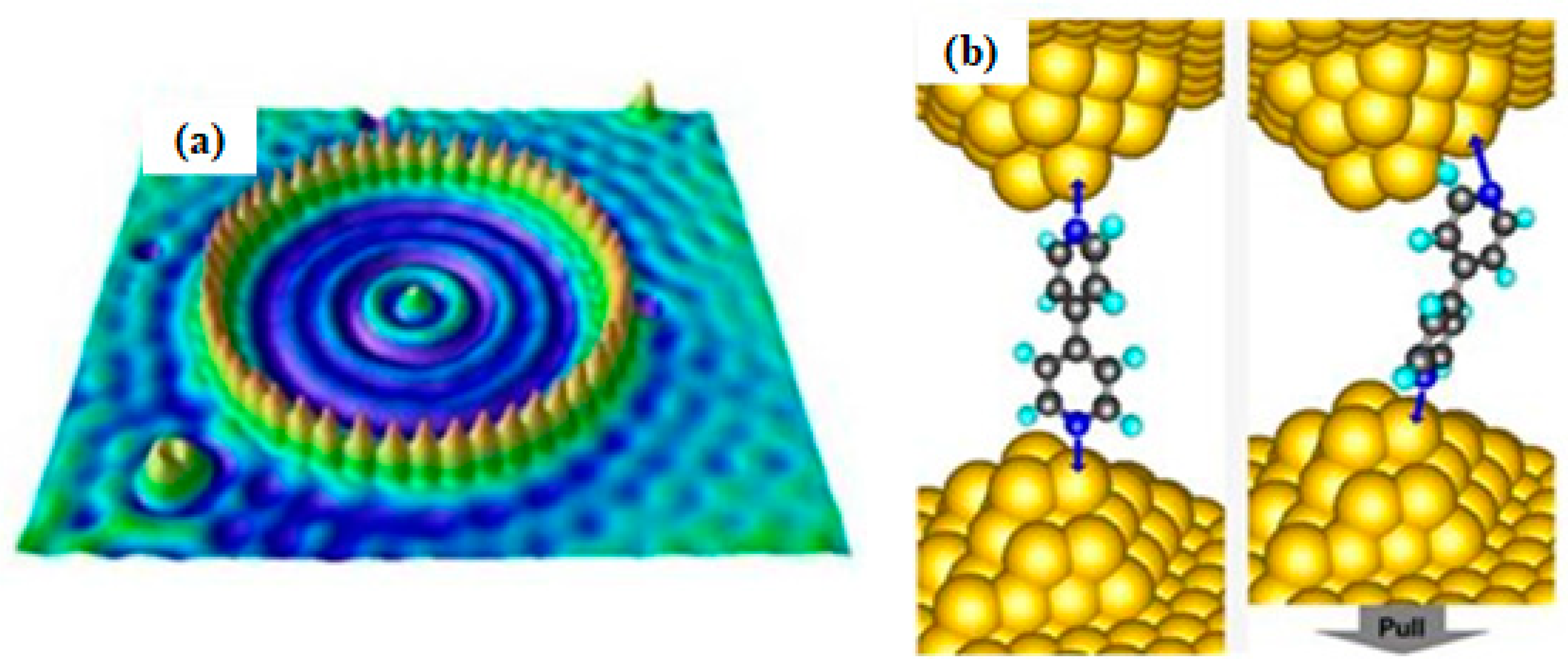
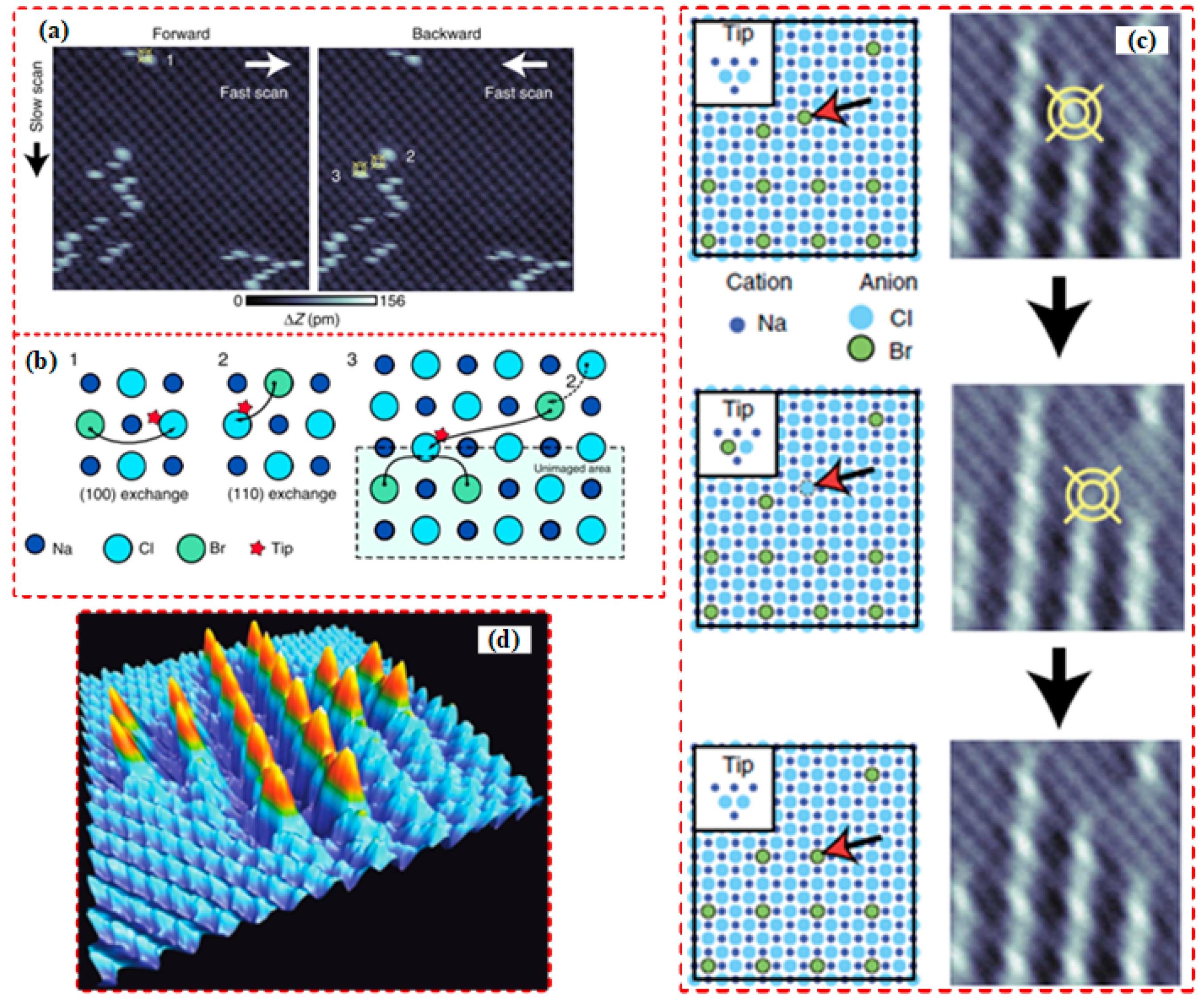
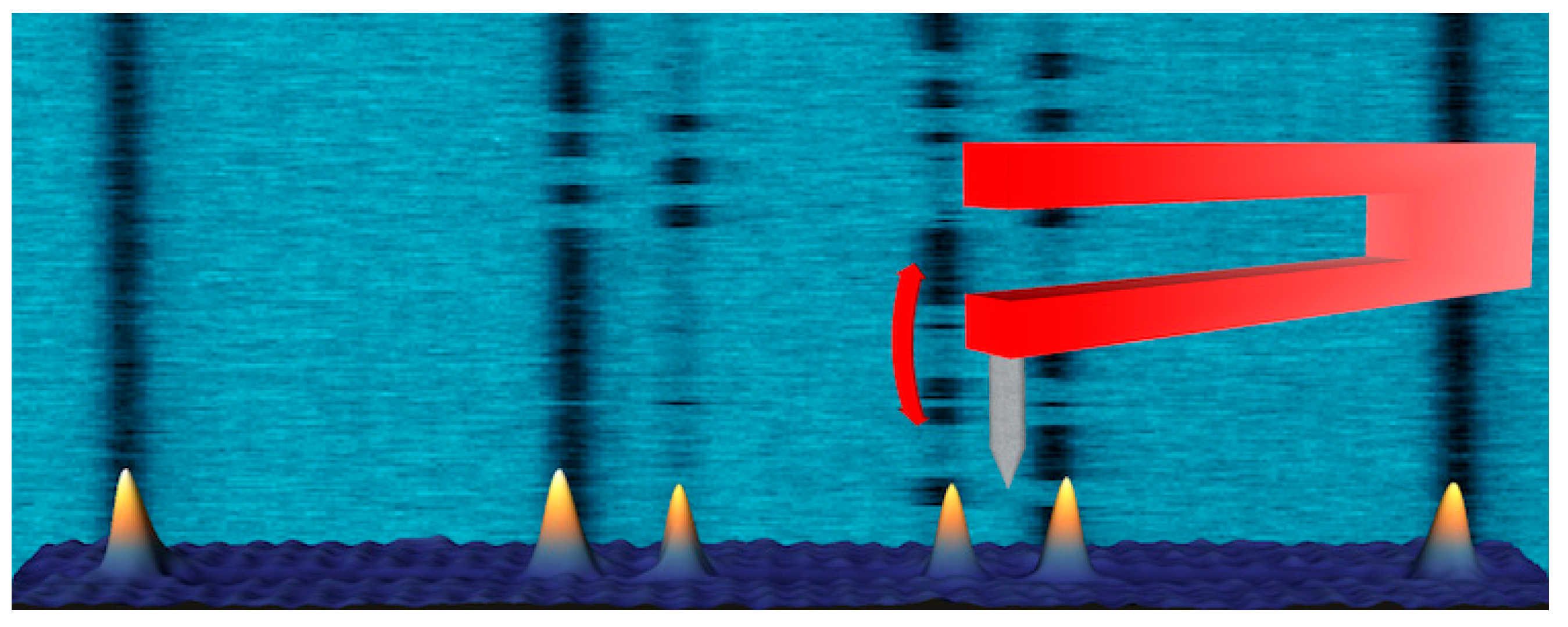
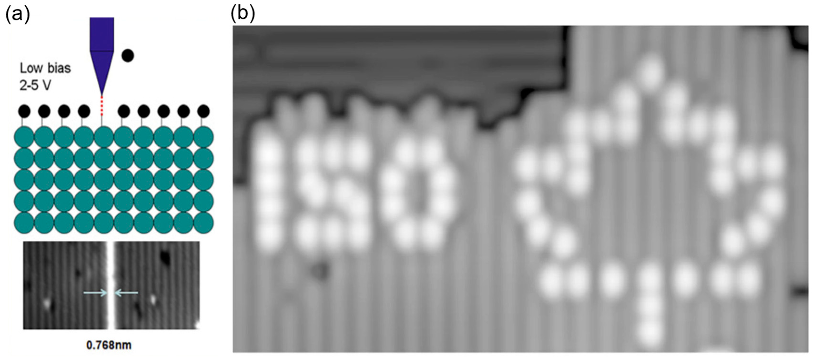
3.1.1. Fabrication Mechanisms
3.1.2. Research Status
3.1.3. Merits and Drawbacks
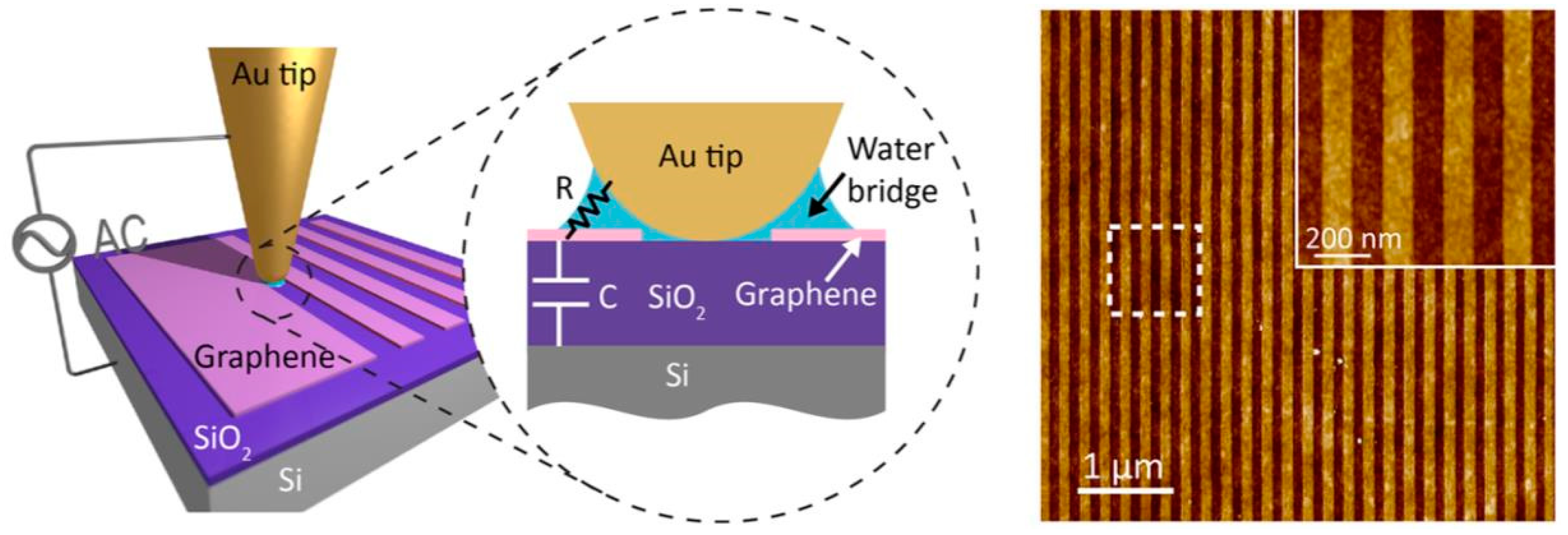
3.2. O-SPL Nanofabrication Approach
3.2.1. Fabrication Mechanism
3.2.2. Research Status
3.2.3. Merits and Drawbacks
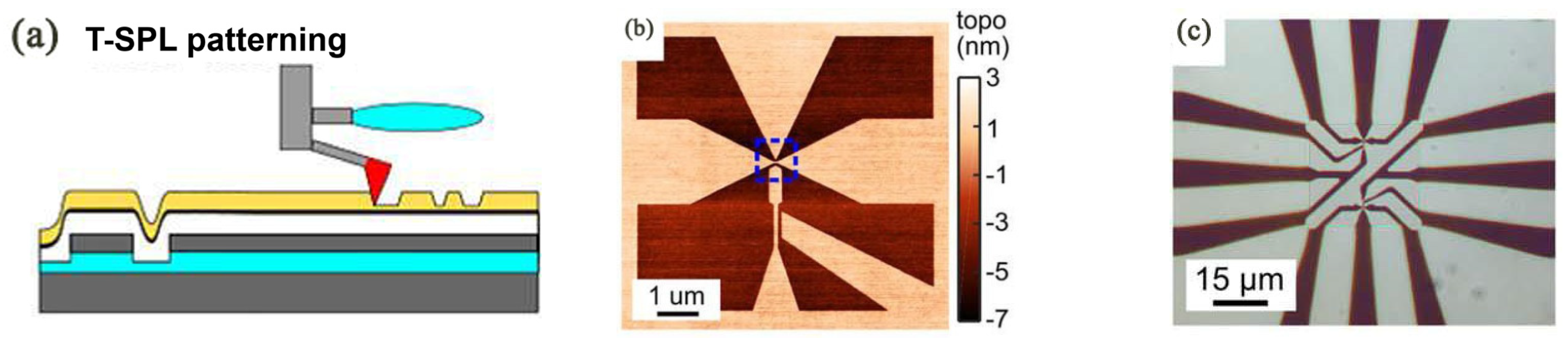
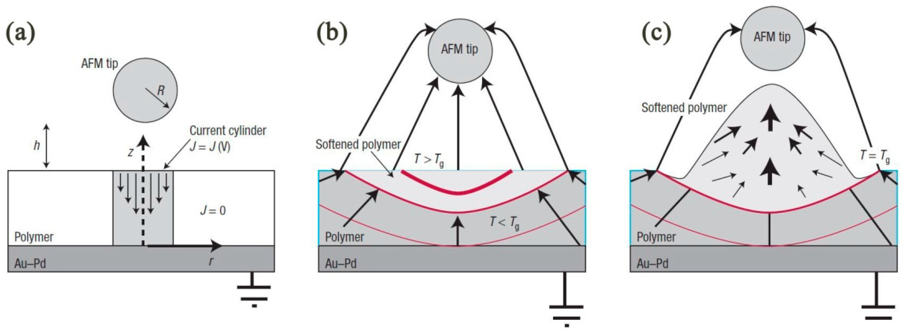
3.3. T-SPL and Tc-SPL Nanofabrication Approach
3.3.1. Fabrication Mechanism
3.3.2. Research Status
3.3.3. Merits and Drawbacks
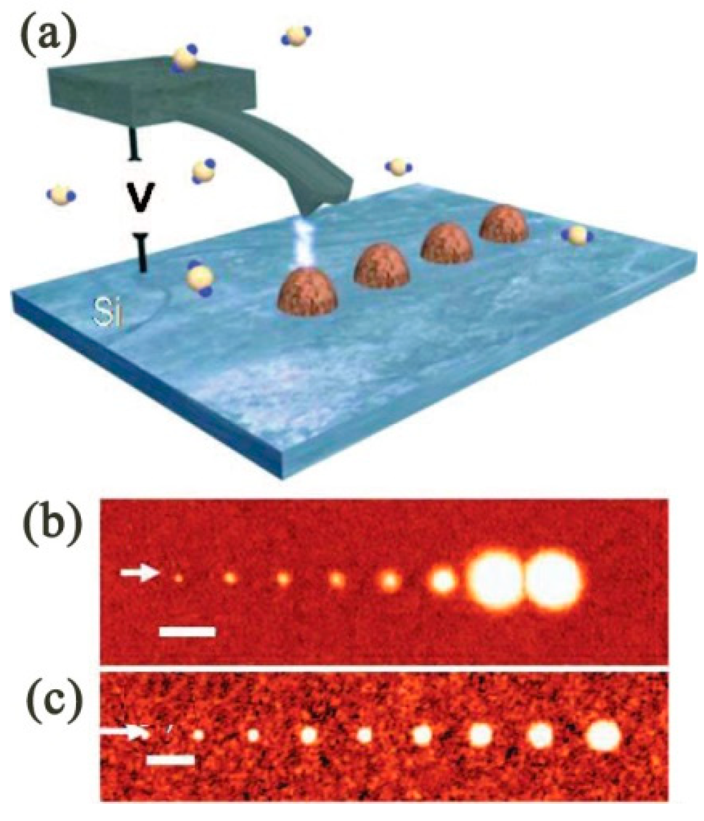
3.4. D-SPL Nanofabrication Approach
3.4.1. Fabrication Mechanism
3.4.2. Research Status
3.4.3. Merits and Drawbacks
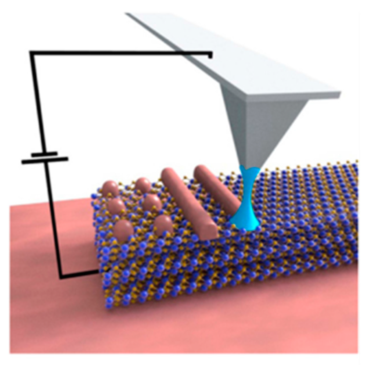
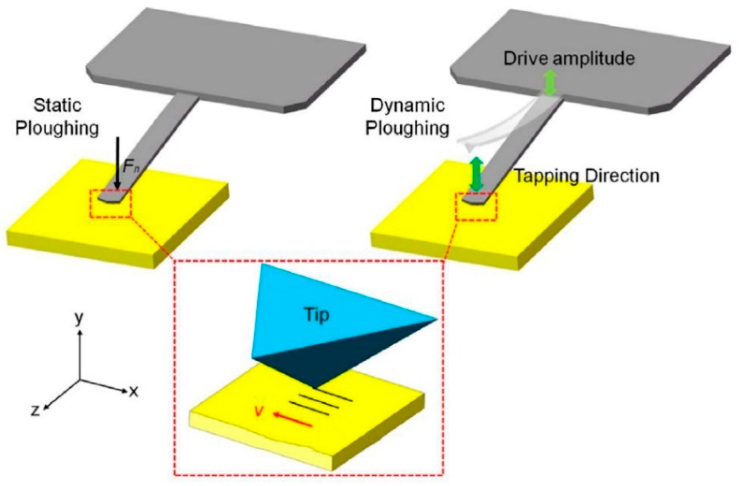
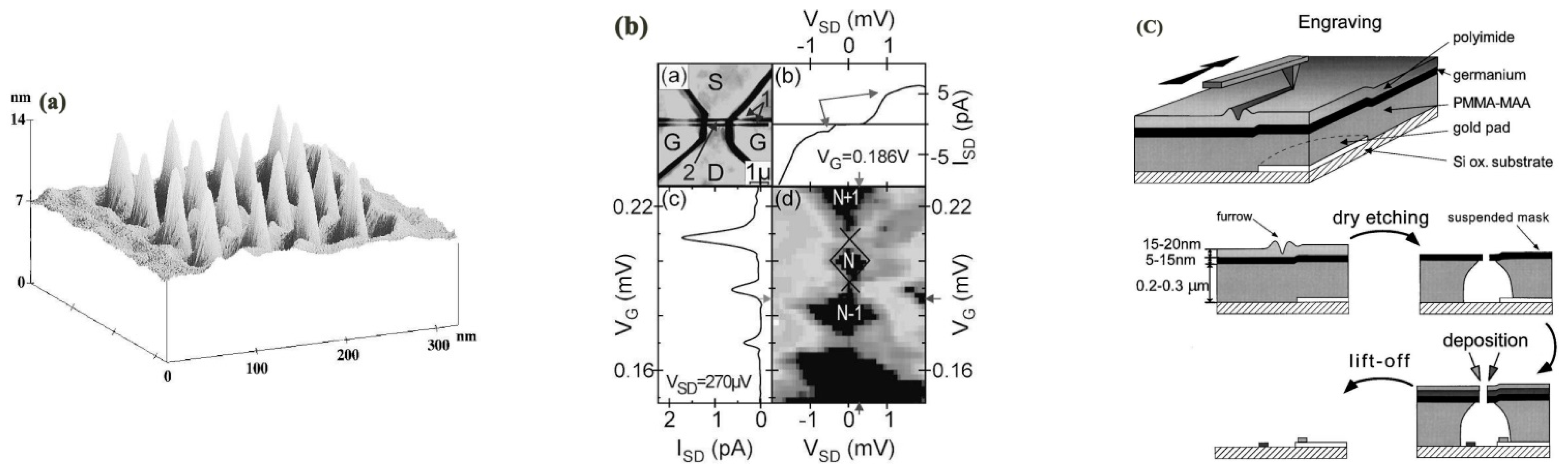
3.5. B-SPL Nanofabrication Approach
3.5.1. Fabrication Mechanism
3.5.2. Research Status
3.5.3. Merits and Drawbacks
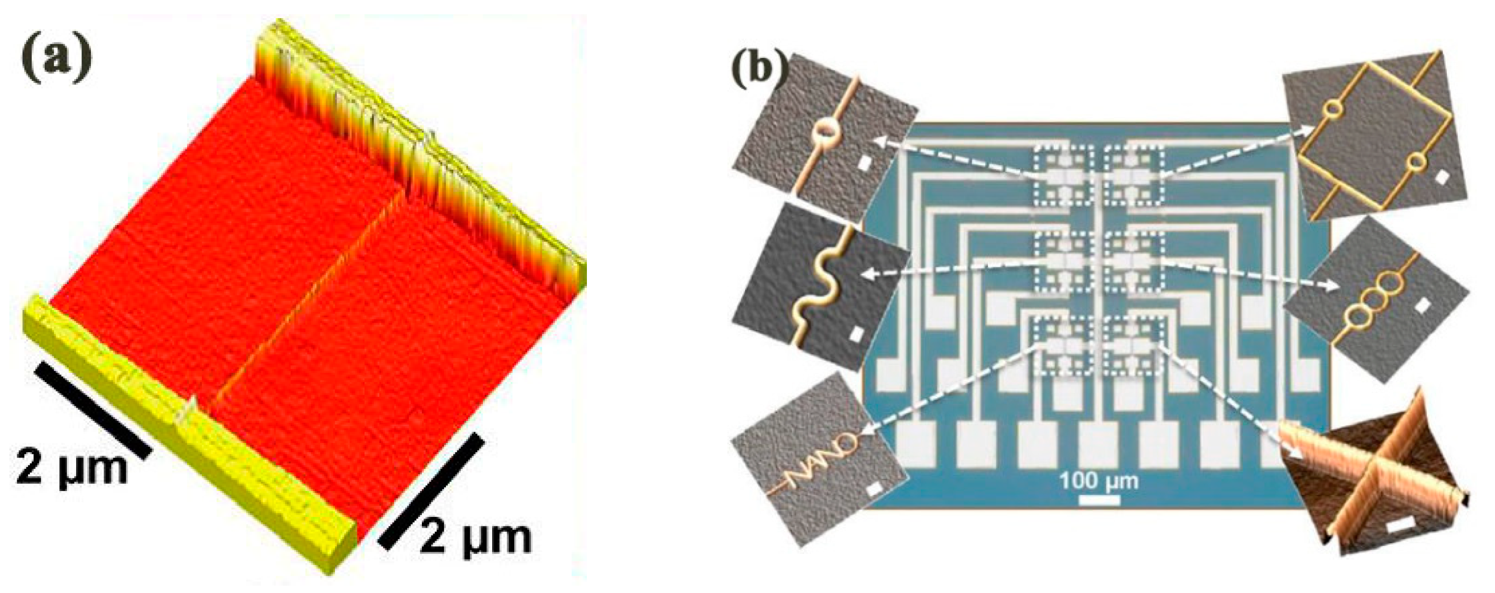
3.6. M-SPL Nanofabrication Approach
3.6.1. Fabrication Mechanism
3.6.2. Research Status
3.6.3. Merits and Drawbacks
3.7. New SPM Tip-Based Nanofabrication Approaches
4. Application of SPL Nanofabrication Technique
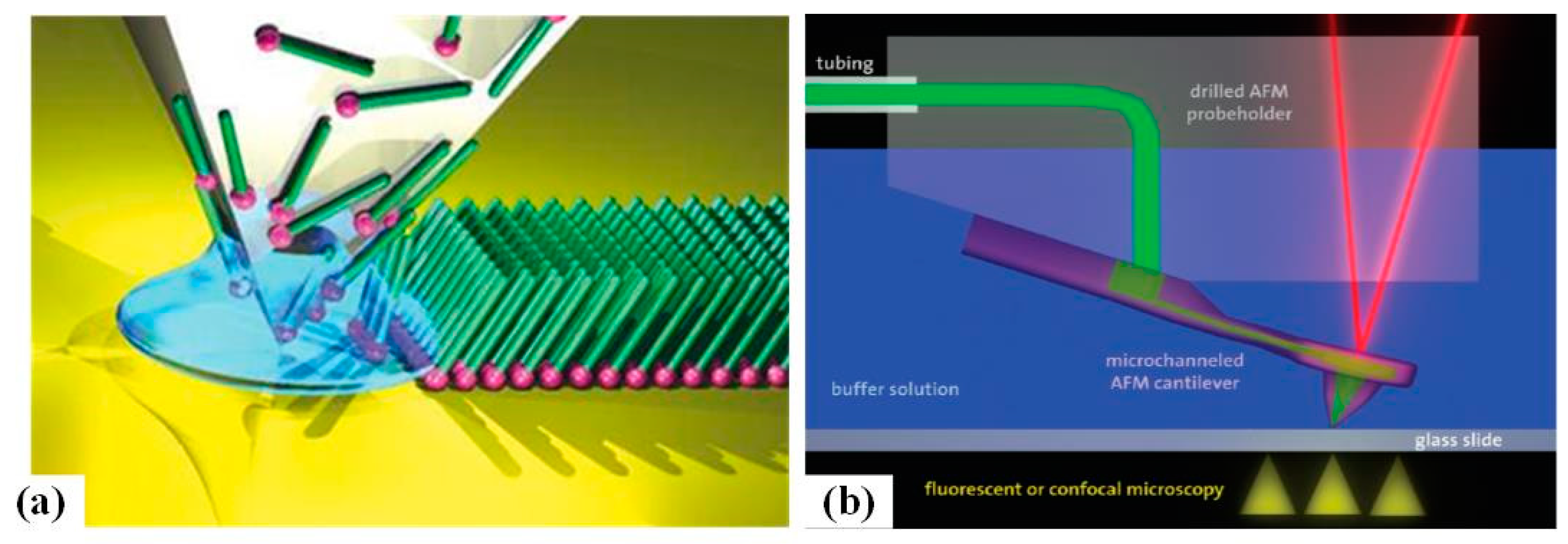
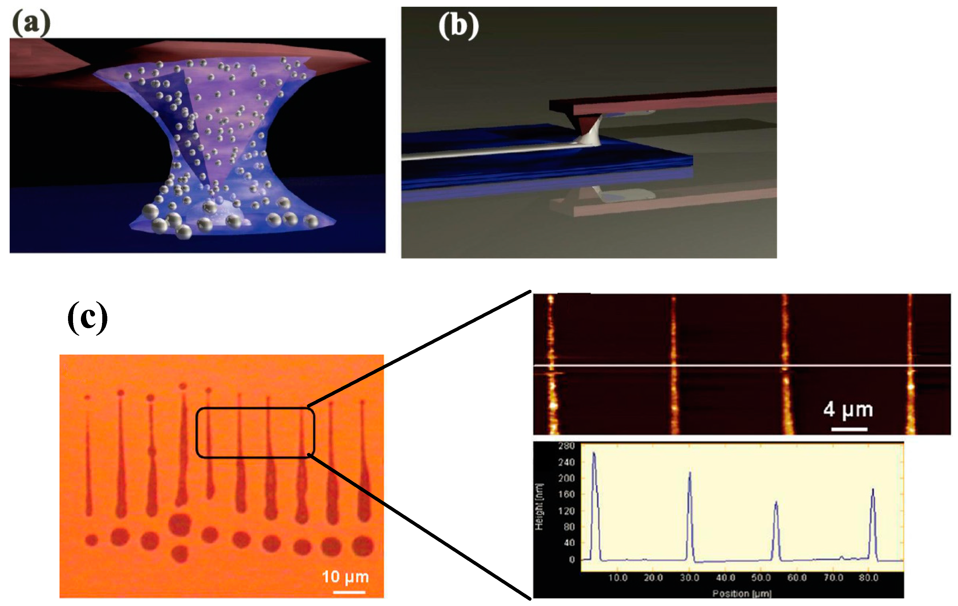
4.1. Nanofluidic Science
4.2. Biomedical Application
4.3. Quantum Computing and Data Storage Device
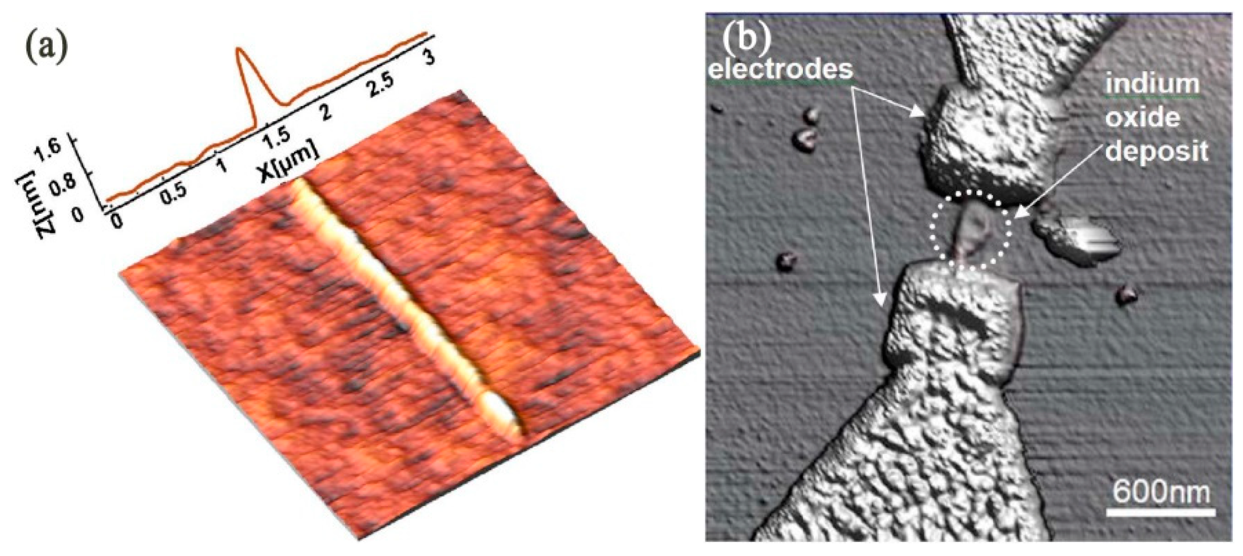
4.4. Nanoelectronics
5. Comparison and Discussion
6. Challenges and Outlook
7. Concluding Remarks
- The SPL nanofabrication technique is a unique technique offering low-cost, high-value manufacturing while achieving atomic-scale precision. It offers additional advantages such as not requiring a mask and allows direct writing on the substrate by means of various chemical, physical, diffusive, and deposition mechanisms.
- The SPL nanofabrication technique has largely been used at the laboratory level to fabricate nanoscale components at a scale envisioned by Nobel Laurette Richard Feynman, and was seen as a long-standing challenge back then even to achieve that level of precision at the nanoscale. With its current success, more efforts are required to enable commercialization of the SPL nanofabrication technique.
- A mix-and-match lithography approach by combining the SPL nanofabrication technique and the etching technique can pave the way to a cost-effective manufacturing method contrary to the currently used mass nanofabrication production techniques.
- The SPL nanofabrication technique is a critical nanofabrication method with great potential to evolve into a disruptive atomic-scale fabrication technology to meet the future demand for atomic manipulation of surfaces.
Funding
Data Availability Statement
Conflicts of Interest
Abbreviations
| SPL | Scanning probe lithography |
| SPM | Scanning probe microscopy |
| FIB | Focused ion beam |
| NIL | Nanoimprint lithography |
| EBL | Electron beam lithography |
| STM | Scanning tunneling microscope |
| AFM | Atomic force microscope |
| EFM | Electrostatic force microscopy |
| MFM | Magnetic force microscopy |
| FluidFM | Fluidic force microscopy |
| PFM | Piezoresponse force microscopy |
| O-SPL | Oxidation scanning probe lithography |
| t-SPL | Thermal scanning probe lithography |
| tc-SPL | Thermochemical scanning probe lithography |
| PMMA | Polymethyl methacrylate |
| PPA | Polypthalaldehyde |
| PPV | p-phenylene vinylene |
| LEDs | Light-emitting diodes |
| D-SPL | Dip-pen scanning probe lithography |
| B-SPL | Bias-induced scanning probe lithography |
| M-SPL | Mechanical scanning probe lithography |
| FFT | Fast Fourier transform |
| SSD | Subsurface damage |
| ASI | Artificial spin ices |
| TB-EBID | Tip-based electron beam-induced deposition |
| PDMS | Polydimethylsiloxane |
| MOSFET | Metal-oxide-semiconductor field-effect transistor |
| FinFET | Fin field-effect transistor |
| SET | Single-electron transistor |
| RT | Room temperature |
| HDL | Hydrogen depassivation lithography |
| APM | Atomically precise manufacturing |
| VMFCL | Voltage-modulated feedback-controlled lithography |
References
- Bayda, S.; Adeel, M.; Tuccinardi, T.; Cordani, M.; Rizzolio, F. The history of nanoscience and nanotechnology: From chemical-physical applications to nanomedicine. Molecules 2020, 25, 112. [Google Scholar] [CrossRef] [PubMed]
- Yan, Y.; Geng, Y.; Hu, Z. Recent advances in AFM tip-based nanomechanical machining. Int. J. Mach. Tools Manuf. 2015, 99, 1–18. [Google Scholar] [CrossRef]
- Fang, F.; Zhang, N.; Guo, D.; Ehmann, K.; Cheung, B.; Liu, K.; Yamamura, K. Towards atomic and close-to-atomic scale manufacturing. Int. J. Extrem. Manuf. 2019, 1, 012001. [Google Scholar] [CrossRef]
- Babu, P.K.V.; Radmacher, M. Mechanics of brain tissues studied by atomic force microscopy: A perspective. Front. Neurosci. 2019, 13, 600. [Google Scholar] [CrossRef] [PubMed]
- Khatri, N.; Barkachary, B.M.; Muneeswaran, B.; Al-Sayegh, R.; Luo, X.; Goel, S. Surface defects incorporated diamond machining of silicon. Int. J. Extrem. Manuf. 2020, 2, 45102. [Google Scholar] [CrossRef]
- Fan, P.; Goel, S.; Luo, X.; Upadhyaya, H.M. Atomic—Scale Friction Studies on Single-Crystal Gallium Arsenide Using Atomic Force Microscope and Molecular Dynamics Simulation. Nanomanuf. Metrol. 2021. [Google Scholar] [CrossRef]
- Gangnaik, A.S.; Georgiev, Y.M.; Collins, G.; Holmes, J.D. Novel germanium surface modification for sub-10 nm patterning with electron beam lithography and hydrogen silsesquioxane resist. J. Vac. Sci. Technol. B Nanotechnol. Microelectron. Mater. Process. Meas. Phenom. 2016, 34, 041603. [Google Scholar] [CrossRef]
- Rajput, N.S.; Luo, X. FIB Micro-/Nano-Fabrication, 2nd ed.; Qin, Y., Ed.; Elsevier: Amsterdam, The Netherlands, 2015. [Google Scholar]
- Takabayashi, Y.; Hiura, M.; Morohoshi, H.; Kodachi, N.; Hayashi, T.; Kimura, A.; Yoshida, T.; Mishima, K.; Suzaki, Y.; Choi, J. Nanoimprint system development for high-volume semiconductor manufacturing the and status of overlay performance. Proc. SPIE 2017, 10144, 1014405. [Google Scholar]
- Gangnaik, A.; Georgiev, Y.M.; McCarthy, B.; Petkov, N.; Djara, V.; Holmes, J.D. Characterisation of a novel electron beam lithography resist, SML and its comparison to PMMA and ZEP resists. Microelectron. Eng. 2014, 123, 126–130. [Google Scholar] [CrossRef]
- Yoo, J.B.; Park, S.-W.; Na Kang, H.; Mondkar, H.S.; Sohn, K.; Kim, H.-M.; Kim, K.-B.; Lee, H. Triphenylsulfonium salt methacrylate bound polymer resist for electron beam lithography. Polymer 2014, 55, 3599–3604. [Google Scholar] [CrossRef]
- Yang, D.X.; Frommhold, A.; Xue, X.; Palmer, R.E.; Robinson, A.P.G. Chemically amplified phenolic fullerene electron beam resist. J. Mater. Chem. C 2014, 2, 1505–1512. [Google Scholar] [CrossRef]
- Yan, J.; Takayama, N. Micro and Nanoscale Laser Processing of Hard Brittle Materials; Elsevier: Amsterdam, The Netherlands, 2020. [Google Scholar]
- Hasan, R.M.M.; Luo, X. Promising Lithography Techniques for Next-Generation Logic Devices. Nanomanuf. Metrol. 2018, 1, 67–81. [Google Scholar] [CrossRef]
- Gangnaik, A.S.; Georgiev, Y.M.; Holmes, J.D. New Generation Electron Beam Resists: A Review. Chem. Mater. 2017, 29, 1898–1917. [Google Scholar] [CrossRef]
- Chen, Y. Nanofabrication by electron beam lithography and its applications: A review. Microelectron. Eng. 2015, 135, 57–72. [Google Scholar] [CrossRef]
- Philip, J.W.M. Focused Ion Beam Microstructuring of Quantum Matter. Annu. Rev. Condens. Matter Phys. 2018, 9, 147–162. [Google Scholar]
- Binnig, G.; Rohrer, H.; Gerber, C.; Weibel, E. Surface studies by scanning tunneling microscopy. Phys. Rev. Lett. 1982, 49, 57–61. [Google Scholar] [CrossRef]
- Eigler, D.M.; Schweizer, E.K. Positioning single atoms with scanning tunnelling microscope. Nature 1990, 344, 524. [Google Scholar] [CrossRef]
- Jung, T.; Moser, A.; Hug, H.; Brodbeck, D.; Hofer, R.; Hidber, H.; Schwarz, U. The atomic force microscope used as a powerful tool for machining surfaces. Ultramicroscopy 1992, 42–44, 1446–1451. [Google Scholar] [CrossRef]
- Tegen, S.; Kracke, B.; Damaschke, B. Surface modifications with a scanning force microscope. Rev. Sci. Instrum. 1997, 68, 1458–1460. [Google Scholar] [CrossRef]
- Weaver, J.M.R. High resolution atomic force microscopy potentiometry. J. Vac. Sci. Technol. B Microelectron. Nanom. Struct. 1991, 9, 1559. [Google Scholar] [CrossRef]
- Hartmann, U. Magnetic force microscopy: Some remarks from the micromagnetic point of view. J. Appl. Phys. 1988, 64, 1561–1564. [Google Scholar] [CrossRef]
- Luo, M.; Yang, W.; Cartwright, T.N.; Higgins, J.M.G.; Chen, J. Simultaneous Measurement of Single-Cell Mechanics and Cell-to-Materials Adhesion Using Fluidic Force Microscopy. Langmuir 2022, 38, 620–628. [Google Scholar] [CrossRef] [PubMed]
- Roelofs, A.; Böttger, U.; Waser, R.; Schlaphof, F.; Trogisch, S.; Eng, L.M. Differentiating 180° and 90° switching of ferroelectric domains with three-dimensional piezoresponse force microscopy. Appl. Phys. Lett. 2000, 77, 3444–3446. [Google Scholar] [CrossRef]
- Lyding, J.W.; Shen, T.C.; Hubacek, J.S.; Tucker, J.R.; Abeln, G.C. Nanoscale patterning and oxidation of H-passivated Si(100)-2 × 1 surfaces with an ultrahigh vacuum scanning tunneling microscope. Appl. Phys. Lett. 1994, 64, 2010–2012. [Google Scholar] [CrossRef]
- Ternes, M.; Lutz, C.P.; Hirjibehedin, C.F.; Giessibl, F.J.; Heinrich, A.J. The Force Needed to Move an Atom on a Surface. Science 2008, 1066, 1066–1070. [Google Scholar] [CrossRef] [PubMed]
- Binnig, G. In Touch with Atoms. Rev. Mod. Phys. 1999, 71, 324–330. [Google Scholar] [CrossRef]
- Repp, J.; Meyer, G.; Olsson, F.E. Controlling the Charge State of individual Gold Adatoms. Science 2004, 305, 493–495. [Google Scholar] [CrossRef]
- Quek, S.Y.; Kamenetska, M.; Steigerwald, M.L.; Choi, H.J.; Louie, S.G.; Hybertsen, M.S.; Neaton, J.B.; Venkataraman, L. Mechanically controlled binary conductance switching of a single-molecule junction. Nat. Nanotechnol. 2009, 4, 230–234. [Google Scholar] [CrossRef]
- Kawai, S.; Foster, A.S.; Canova, F.F.; Onodera, H.; Kitamura, S.I.; Meyer, E. Atom manipulation on an insulating surface at room temperature. Nat. Commun. 2014, 5, 4403. [Google Scholar] [CrossRef]
- Sugimoto, Y.; Abe, M.; Hirayama, S.; Oyabu, N.; Custance, O.; Morita, S. Atom inlays performed at room temperature using atomic force microscopy. Nat. Mater. 2005, 4, 156–159. [Google Scholar] [CrossRef]
- Rashidi, M.; Vine, W.; Dienel, T.; Livadaru, L.; Retallick, J.; Huff, T.; Walus, K.; Wolkow, R.A. Initiating and Monitoring the Evolution of Single Electrons Within Atom-Defined Structures. Phys. Rev. Lett. 2018, 121, 166801. [Google Scholar] [CrossRef] [PubMed]
- Randall, J.N.; Lyding, J.W.; Schmucker, S.; Von Ehr, J.R.; Ballard, J.; Saini, R.; Xu, H.; Ding, Y. Atomic precision lithography on Si. J. Vac. Sci. Technol. B Microelectron. Nanom. Struct. 2009, 27, 2764. [Google Scholar] [CrossRef]
- Randall, J.N.; Owen, J.H.; Fuchs, E.; Lake, J.; Von Ehr, J.R.; Ballard, J.; Henriksen, E. Digital atomic scale fabrication an inverse Moore’s Law—A path to atomically precise manufacturing. Micro Nano Eng. 2018, 1, 1–14. [Google Scholar] [CrossRef]
- Moheimani, S.O.R.; Alemansour, H. A new approach to removing H atoms in hydrogen depassivation lithography. Proc. SPIE 2020, 11324, 113240Y. [Google Scholar]
- Rashidi, M.; Croshaw, J.; Mastel, K.; Tamura, M.; Hosseinzadeh, H.; Wolkow, R.A. Deep learning-guided surface characterization for autonomous hydrogen lithography. Mach. Learn. Sci. Technol. 2020, 1, 025001. [Google Scholar] [CrossRef]
- Schofield, S.R.; Curson, N.J.; Simmons, M.Y.; Rueß, F.J.; Hallam, T.; Oberbeck, L.; Clark, R.G. Atomically precise placement of single dopants in si. Phys. Rev. Lett. 2003, 91, 2–5. [Google Scholar] [CrossRef]
- Scappucci, G.; Capellini, G.; Lee, W.C.T.; Simmons, M.Y. Atomic-scale patterning of hydrogen terminated Ge(001) by scanning tunneling microscopy. Nanotechnology 2009, 20, 495302. [Google Scholar] [CrossRef]
- Miwa, J.A.; Simmons, M.Y. Atomic-Scale Devices in Silicon by Scanning Tunneling Microscopy. In Atomic Scale Interconnection Machines; Springer: Berlin/Heidelberg, Germany, 2012; pp. 181–196. [Google Scholar]
- Lyding, J.W. Nanometer scale patterning and oxidation of silicon surfaces with an ultrahigh vacuum scanning tunneling microscope. J. Vac. Sci. Technol. B Microelectron. Nanom. Struct. 1994, 12, 3735–3740. [Google Scholar] [CrossRef]
- Kruse, P.; Wolkow, R.A. ‘Gentle lithography’ with benzene on Si(100). Appl. Phys. Lett. 2002, 81, 4422–4424. [Google Scholar] [CrossRef]
- Walsh, M.A.; Hersam, M.C. Atomic-scale templates patterned by ultrahigh vacuum scanning tunneling microscopy on silicon. Annu. Rev. Phys. Chem. 2009, 60, 193–216. [Google Scholar] [CrossRef]
- Pavlova, T.V.; Shevlyuga, V.M.; Andryushechkin, B.V.; Zhidomirov, G.M.; Eltsov, K.N. Local removal of silicon layers on Si(100)-2 × 1 with chlorine-resist STM lithography. Appl. Surf. Sci. 2020, 509, 145235. [Google Scholar] [CrossRef]
- Dwyer, K.J.; Dreyer, M.; Butera, R.E. STM-Inuce Desorption an Lithographic Patterning of Cl-Si(100)-(2 × 1). J. Phys. Chem. A 2019, 123, 10793–10803. [Google Scholar] [CrossRef] [PubMed]
- Fuechsle, M.; Miwa, J.; Mahapatra, S.; Ryu, H.; Lee, S.; Warschkow, O.; Hollenberg, L.; Klimeck, G.; Simmons, M. A single-atom transistor. Nat. Nanotechnol. 2012, 7, 242–246. [Google Scholar] [CrossRef] [PubMed]
- Bussmann, E.; Butera, R.E.; Owen, J.H.G.; Randall, J.N.; Rinaldi, S.M.; Baczewski, A.D.; Misra, S. Atomic-precision advanced manufacturing for Si quantum computing. MRS Bull. 2021, 46, 607–615. [Google Scholar] [CrossRef]
- Livadaru, L.; Xue, P.; Shaterzadeh-Yazdi, Z.; DiLabio, G.A.; Mutus, J.; Pitters, J.L.; Sanders, B.C.; Wolkow, R.A. Dangling-bond charge qubit on a silicon surface. New J. Phys. 2010, 12, 083018. [Google Scholar] [CrossRef]
- Simmons, M.Y. Quantum computing in silicon. In Proceedings of the 2015 IEEE International Electron Devices Meeting (IEDM), Washington, DC, USA, 7–9 December 2015; pp. 1.2.1–1.2.4. [Google Scholar]
- Achal, R.; Rashidi, M.; Croshaw, J.; Churchill, D.; Taucer, M.; Huff, T.; Cloutier, M.; Pitters, J.; Wolkow, R.A. Lithography for robust and editable atomic-scale silicon devices and memories. Nat. Commun. 2018, 9, 2778. [Google Scholar] [CrossRef]
- Kirk, W.P.; Randall, J.N.; Owen, J.H.G. 2D Quantum Metamaterials; World Scientific: Gaithersburg, MD, USA, 2019. [Google Scholar]
- Randall, J.N.; Owen, J.H.G.; Lake, J.; Saini, R.; Fuchs, E.; Mahdavi, M.; Moheimani, S.O.R.; Schaefer, B.C. Highly parallel scanning tunneling microscope based hydrogen depassivation lithography. J. Vac. Sci. Technol. B 2018, 36, 06JL05. [Google Scholar] [CrossRef]
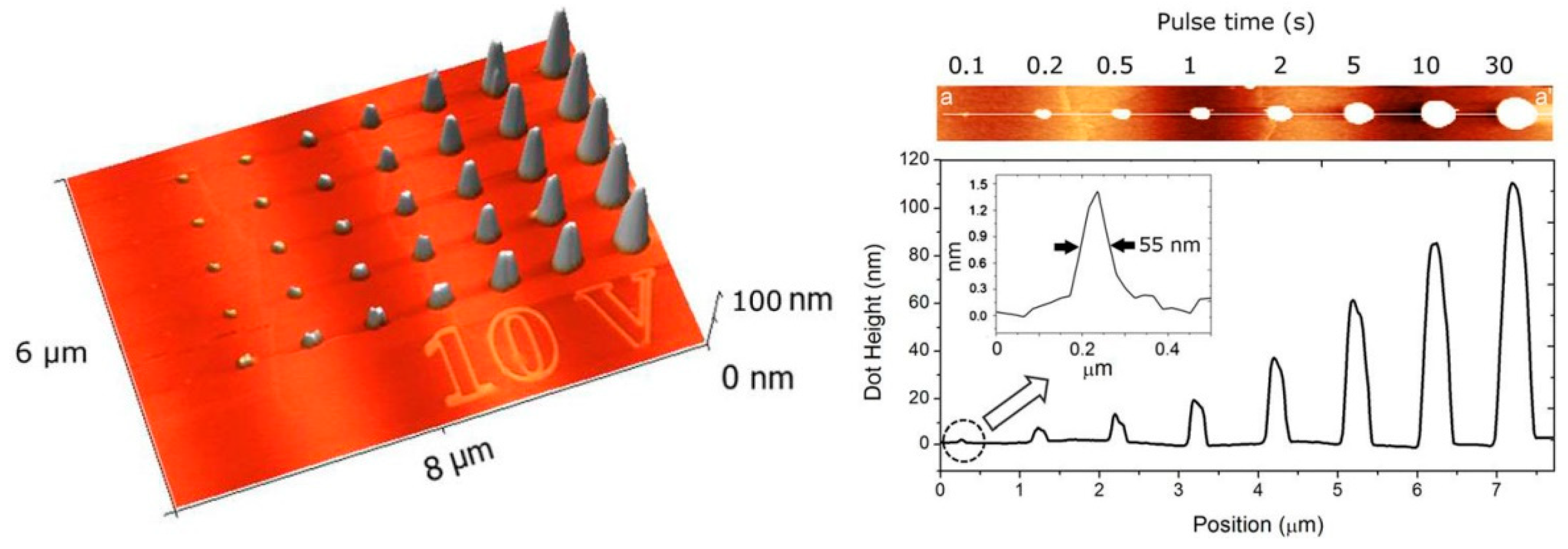
- Dagata, J.A. SPM-Based Lithography for Electronics Device Fabrication: New Strategies and Directions. MRS Online Proc. Libr. 1995, 380, 153–162. [Google Scholar] [CrossRef]
- Dagata, J.A. Device Fabrication by Scanned robe Oxidation cessing by wet dry a chemical is Small RNA Chaperones for Ribosome Biogenesis. Science 1995, 270, 1625–1627. [Google Scholar] [CrossRef]
- Cramer, T.; Zerbetto, F.; García, R. Molecular mechanism of water bridge buildup: Field-induced formation of nanoscale menisci. Langmuir 2008, 24, 6116–6120. [Google Scholar] [CrossRef]
- Garcia, R.; Martinez, R.V.; Martinez, J. Nano-chemistry and scanning probe nanolithographies. Chem. Soc. Rev. 2006, 35, 29–38. [Google Scholar] [CrossRef] [PubMed]
- Ryu, Y.K.; Garcia, R. Advanced oxidation scanning probe lithography. Nanotechnology 2017, 28, 142003. [Google Scholar] [CrossRef] [PubMed]
- Germain, J.; Rolandi, M.; Backer, S.A.; Fréchet, J.M.J. Sulfur as a novel nanopatterning material: An ultrathin resist and a chemically addressable template for nanocrystal self-assembly. Adv. Mater. 2008, 20, 4526–4529. [Google Scholar] [CrossRef]
- Weng, L.; Zhang, L.; Chen, Y.P.; Rokhinson, L.P. Atomic force microscope local oxidation nanolithography of graphene. Appl. Phys. Lett. 2008, 93, 093107. [Google Scholar] [CrossRef]
- Martinez, J.; Martínez, R.V.; Garcia, R. Silicon nanowire transistors with a channel width of 4 nm fabricated by atomic force microscope nanolithography. Nano Lett. 2008, 8, 3636–3639. [Google Scholar] [CrossRef]
- Li, H.; Ying, Z.; Lyu, B.; Deng, A.; Wang, L.; Taniguchi, T.; Watanabe, K.; Shi, Z. Electrode-Free Anodic Oxidation Nanolithography of Low-Dimensional Materials. Nano Lett. 2018, 18, 8011–8015. [Google Scholar] [CrossRef]
- Martínez, R.V.; Martínez, J.; Garcia, R. Silicon nanowire circuits fabricated by AFM oxidation nanolithography. Nanotechnology 2010, 21, 245301. [Google Scholar] [CrossRef]
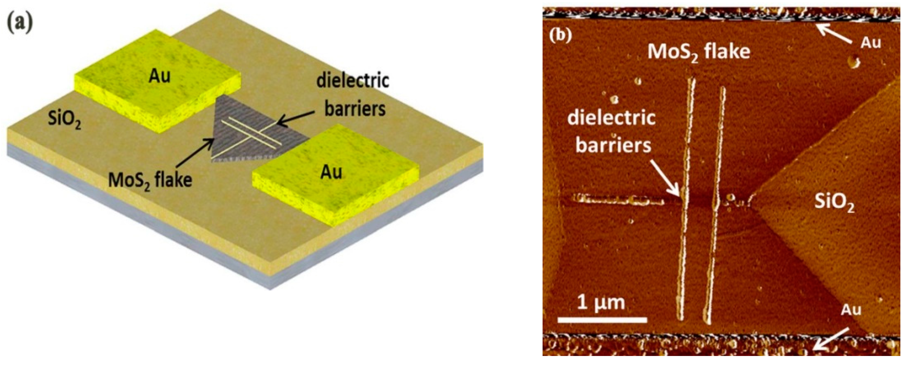
- Espinosa, F.M.; Ryu, Y.K.; Marinov, K.; Dumcenco, D.; Kis, A.; Garcia, R. Direct fabrication of thin layer MoS2field-effect nanoscale transistors by oxidation scanning probe lithography. Appl. Phys. Lett. 2015, 106, 103503. [Google Scholar] [CrossRef]
- Bertolazzi, S.; Krasnozhon, D.; Kis, A. Nonvolatile memory cells based on MoS2/graphene heterostructures. ACS Nano 2013, 7, 3246–3252. [Google Scholar] [CrossRef]
- Wang, L.; Wang, Y.; Wong, J.I.; Palacios, T.; Kong, J.; Yang, H.Y. Functionalized MoS2nanosheet-based field-effect biosensor for label-free sensitive detection of cancer marker proteins in solution. Small 2014, 10, 1101–1105. [Google Scholar] [CrossRef]
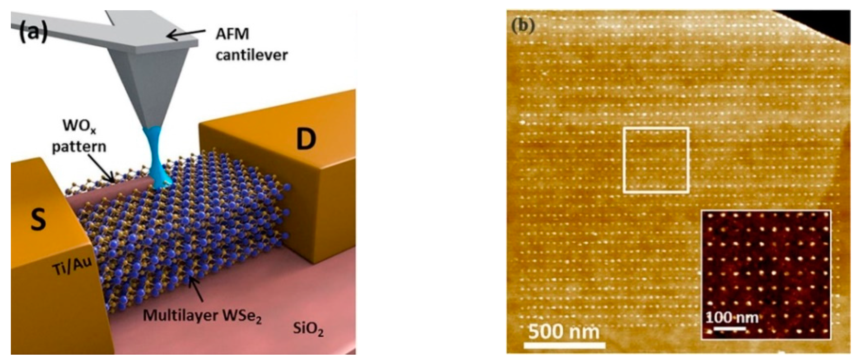
- Dago, A.I.; Ryu, Y.K.; Garcia, R. Sub-20 nm patterning of thin layer WSe2 by scanning probe lithography. Appl. Phys. Lett. 2016, 109, 163103. [Google Scholar] [CrossRef]
- Lorenzoni, M.; Torre, B. Scanning probe oxidation of SiC, fabrication possibilities and kinetics considerations. Appl. Phys. Lett. 2013, 103, 163109. [Google Scholar] [CrossRef]
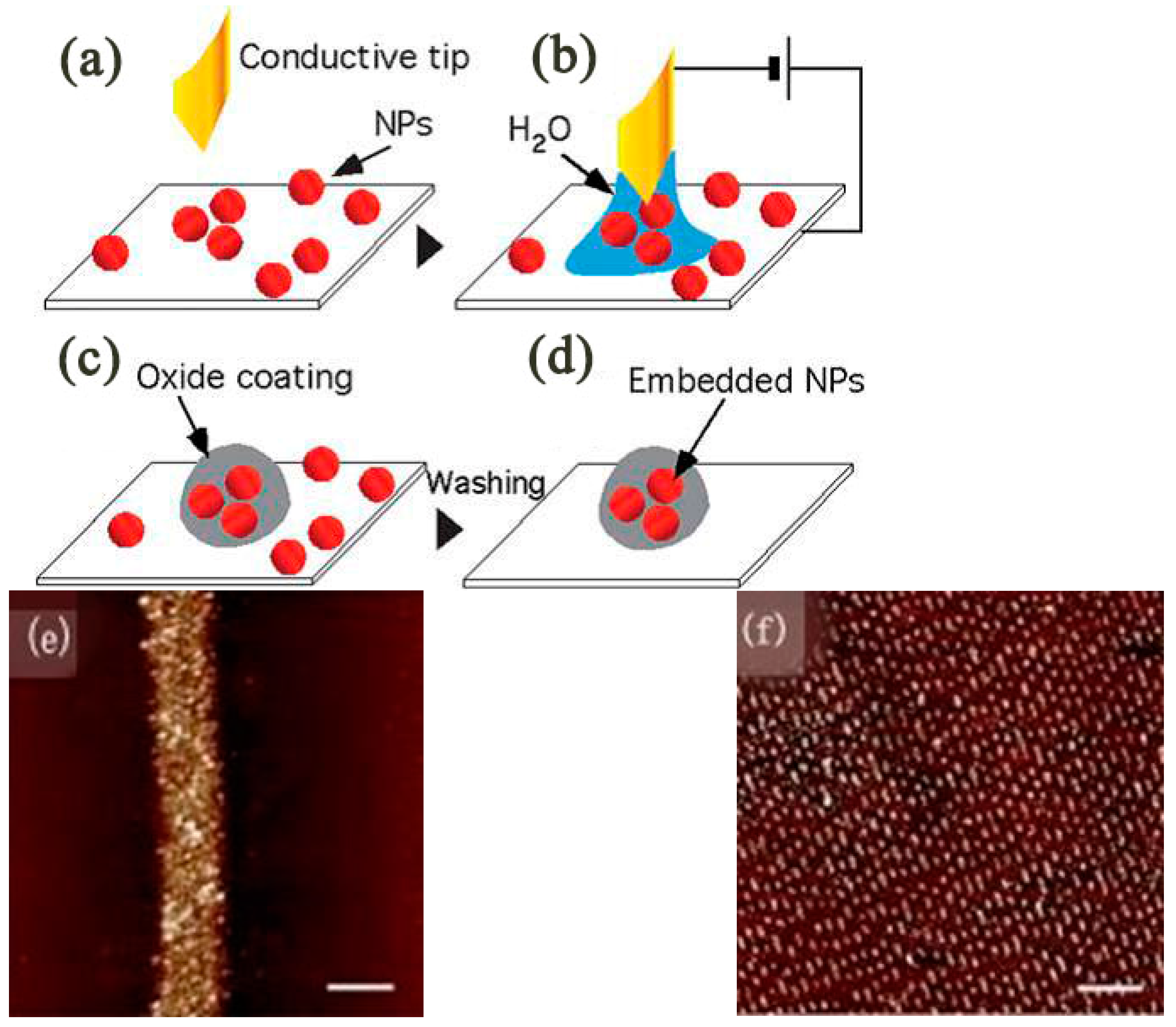
- Cavallini, M.; Simeone, F.C.; Borgatti, F.; Albonetti, C.; Morandi, V.; Sangregorio, C.; Innocenti, C.; Pineider, F.; Annese, E.; Panaccione, G.; et al. Additive nanoscale embedding of functional nanoparticles on silicon surface. Nanoscale 2010, 2, 2069–2072. [Google Scholar] [CrossRef] [PubMed]
- Lee, J.; Wright, T.L.; Abel, M.R.; Sunden, E.O.; Marchenkov, A.; Graham, S.; King, W.P. Thermal conduction from microcantilever heaters in partial vacuum. J. Appl. Phys. 2007, 101, 014906. [Google Scholar] [CrossRef]
- Mamin, H.J.; Rugar, D. Thermomechanical writing with an atomic force microscope tip. Appl. Phys. Lett. 1992, 61, 1003–1005. [Google Scholar] [CrossRef]
- Cavallini, M.; Simeone, F.C.; Borgatti, F.; Albonetti, C.; Morandi, V.; Sangregorio, C.; Innocenti, C.; Pineider, F.; Annese, E.; Panaccione, G.; et al. Direct writing and characterization of poly(p-phenylene vinylene) nanostructures. Appl. Phys. Lett. 2009, 95, 93–96. [Google Scholar]
- Lee, B.; Prater, C.B.; King, W.P. Lorentz force actuation of a heated atomic force microscope cantilever. Nanotechnology 2012, 23, 055709. [Google Scholar] [CrossRef]
- Lee, J.; Beechem, T.; Wright, T.L.; Nelson, B.A.; Graham, S.; King, W.P. Electrical, thermal, and mechanical characterization of silicon microcantilever heaters. J. Microelectromech. Syst. 2006, 15, 1644–1655. [Google Scholar] [CrossRef]
- Garcia, R.; Knoll, A.W.; Riedo, E. Advanced scanning probe lithography. Nat. Nanotechnol. 2014, 9, 577–587. [Google Scholar] [CrossRef]
- Pires, D.; Hedrick, J.L.; De Silva, A.; Frommer, J.; Gotsmann, B.; Wolf, H.; Despont, M.; Duerig, U.; Knoll, A.W. Nanoscale Three-Dimensional Patterning of Molecular Resists by Scanning Probes. Science 2010, 328, 732–735. [Google Scholar] [CrossRef]
- Shaw, J.E.; Stavrinou, P.N.; Anthopoulos, T.D. On-demand patterning of nanostructured pentacene transistors by scanning thermal lithography. Adv. Mater. 2013, 25, 552–558. [Google Scholar] [CrossRef] [PubMed]
- Lee, W.-K.; Robinson, J.T.; Gunlycke, D.; Stine, R.R.; Tamanaha, C.R.; King, W.P.; Sheehan, P.E. Chemically isolated graphene nanoribbons reversibly formed in fluorographene using polymer nanowire masks. Nano Lett. 2011, 11, 5461–5464. [Google Scholar] [CrossRef] [PubMed]
- Liu, X.; Howell, S.T.; Conde-Rubio, A.; Boero, G.; Brugger, J. Thermomechanical Nanocutting of 2D Materials. Adv. Mater. 2020, 32, 2001232. [Google Scholar] [CrossRef] [PubMed]
- Wei, Y.; Liu, P.; Zhu, F.; Jiang, K.; Li, Q.; Fan, S. Efficient fabrication of carbon nanotube micro tip arrays by tailoring cross-stacked carbon nanotube sheets. Nano Lett. 2012, 12, 2071–2076. [Google Scholar] [CrossRef]
- Zimmermann, S.T.; Balkenende, D.W.R.; Lavrenova, A.; Weder, C.; Brugger, J. Nanopatterning of a Stimuli-Responsive Fluorescent Supramolecular Polymer by Thermal Scanning Probe Lithography. ACS Appl. Mater. Interfaces 2017, 9, 41454–41461. [Google Scholar] [CrossRef]
- Mamin, H.J. Thermal writing using a heated atomic force microscope tip. Appl. Phys. Lett. 1996, 69, 433–435. [Google Scholar] [CrossRef]
- Gotsmann, B.; Dürig, U. Thermally Activated Nanowear Modes of a Polymer Surface Induced by a Heated Tip. Langmuir 2004, 20, 1495–1500. [Google Scholar] [CrossRef]
- RGriffiths, A.; Williams, A.; Servin, I.; Tiron, R. Corrigendum: Thermal scanning probe lithography for the directed self- assembly of block copolymers. Nanotechnology 2017, 28, 175301. [Google Scholar]
- Kim, H.J.; Moldovan, N.; Felts, J.R.; Somnath, S.; Dai, Z.; Jacobs, T.D.B.; Carpick, R.W.; Carlisle, J.A.; King, W.P. Ultrananocrystalline diamond tip integrated onto a heated atomic force microscope cantilever. Nanotechnology 2012, 23, 495302. [Google Scholar] [CrossRef]
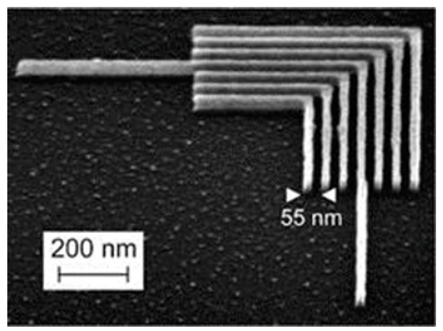
- Cho, Y.K.R.; Rawlings, C.D.; Wolf, H.; Spieser, M.; Bisig, S.; Reidt, S.; Sousa, M.; Khanal, S.R.; Jacobs, T.D.B.; Knoll, A.W. Sub-10 Nanometer Feature Size in Silicon Using Thermal Scanning Probe Lithography. ACS Nano 2017, 11, 11890–11897. [Google Scholar]
- Cheong, L.L.; Paul, P.; Holzner, F.; Despont, M.; Coady, D.J.; Hedrick, J.L.; Allen, R.; Knoll, A.W.; Duerig, U. Thermal probe maskless lithography for 27.5 nm half-pitch Si technology. Nano Lett. 2013, 13, 4485–4491. [Google Scholar] [CrossRef] [PubMed]
- Rawlings, C.D.; Ryu, Y.K.; Rüegg, M.; Lassaline, N.; Schwemmer, C.; Duerig, U.; Knoll, A.W.; Durrani, Z.A.K.; Wang, C.; Liu, D.; et al. Fast turnaround fabrication of silicon point-contact quantum-dot transistors using combined thermal scanning probe lithography and laser writing. Nanotechnology 2018, 29, 505302. [Google Scholar] [CrossRef] [PubMed]
- Shaw, J.E.; Stavrinou, P.N.; Anthopoulos, T.D. High-speed scanning thermal lithography for nanostructuring of electronic devices. Nanoscale 2014, 6, 5813–5819. [Google Scholar] [CrossRef] [PubMed]
- Ellington, A.D.; Szostak, J.W. Light-emiting diodes based on conjugated polymers. Nature 1990, 346, 818–822. [Google Scholar] [CrossRef]
- Fenwick, O.; Bozec, L.; Credgington, D.; Hammiche, A.; Lazzerini, G.M.; Silberberg, Y.R.; Cacialli, F. Thermochemical nanopatterning of organic semiconductors. Nat. Nanotechnol. 2009, 4, 664–668. [Google Scholar] [CrossRef] [PubMed]
- Howell, S.T.; Grushina, A.; Holzner, F.; Brugger, J. Thermal scanning probe lithography—A review. Microsyst. Nanoeng. 2020, 6, 21. [Google Scholar] [CrossRef] [PubMed]
- Vettiger, P.; Cross, G.; Despont, M.; Drechsler, U.; Durig, U.; Gotsmann, B.; Haberle, W.; Lantz, M.; Rothuizen, H.; Stutz, R.; et al. The ‘millipede’-nanotechnology entering data storage. IEEE Trans. Nanotechnol. 2002, 1, 39–54. [Google Scholar] [CrossRef]
- Lim, J.H.; Mirkin, C.A. Electrostatically driven Dip-pen nanolithography of conducting polymers. Adv. Mater. 2002, 14, 1474–1477. [Google Scholar] [CrossRef]
- Maynor, B.W.; Filocamo, S.F.; Grinstaff, M.W.; Liu, J. Direct-writing of polymer nanostructures: Poly(thiophene) nanowires on semiconducting and insulating surfaces. J. Am. Chem. Soc. 2002, 124, 522–523. [Google Scholar] [CrossRef]
- Ginger, D.S.; Zhang, H.; Mirkin, C.A. The Evolution of Dip-Pen Nanolithography. Angew. Chem. Int. Ed. 2004, 43, 30–45. [Google Scholar] [CrossRef]
- Zhou, X.; He, S.; Brown, K.A.; Mendez-Arroyo, J.; Boey, F.; Mirkin, C.A. Locally altering the electronic properties of graphene by nanoscopically doping it with rhodamine 6G. Nano Lett. 2013, 13, 1616–1621. [Google Scholar] [CrossRef] [PubMed]
- Zhao, J.; Swartz, L.A.; Lin, W.-F.; Schlenoff, P.S.; Frommer, J.; Schlenoff, J.B.; Liu, G.-Y. Three-Dimensional Nanoprinting via Scanning Probe Lithography-Delivered Layer-by-Layer Deposition. ACS Nano 2016, 10, 5656–5662. [Google Scholar] [CrossRef] [PubMed]
- Bellido, E.; de Miguel, R.; Sesé, J.; Ruiz-Molina, D.; Lostao, A.; Maspoch, D. Nanoscale positioning of inorganic nanoparticles using biological ferritin arrays fabricated by Dip-Pen Nanolithography. Scanning 2010, 32, 35–41. [Google Scholar] [CrossRef] [PubMed]
- Lee, K.-B.; Park, S.-J.; Mirkin, C.A.; Smith, J.C.; Mrksich, M. Protein Nanoarrays Generated By Dip-Pen Nanolithography. Science 2002, 295, 1702–1705. [Google Scholar] [CrossRef] [PubMed]
- Kuljanishvili, I.; Dikin, D.A.; Rozhok, S.; Mayle, S.; Chandrasekhar, V. Controllable patterning and CVD growth of isolated carbon nanotubes with direct parallel writing of catalyst using dip-pen Nanolithography. Small 2009, 5, 2523–2527. [Google Scholar] [CrossRef] [PubMed]
- Jewell, C.M.; Lynn, D.M. Multilayered polyelectrolyte assemblies as platforms for the delivery of DNA and other nucleic acid-based therapeutics. Adv. Drug Deliv. Rev. 2008, 60, 979–999. [Google Scholar] [CrossRef]
- Wu, C.; Reinhoudt, D.N.; Otto, C.; Velders, A.H.; Subramaniam, V. Protein Immobilization on Ni (II) Ion Patterns Prepared by Microcontact Printing and Dip-Pen Nanolithography. ACS Nano 2010, 4, 1083–1091. [Google Scholar] [CrossRef]
- Chung, S.; Felts, J.R.; Wang, D.; King, W.P.; de Yoreo, J.J. Temperature-dependence of ink transport during thermal dip-pen nanolithography. Appl. Phys. Lett. 2011, 99, 193101. [Google Scholar] [CrossRef]
- Salaita, K.; Wang, Y.; Mirkin, C.A. Applications of dip-pen nanolithography. Nat. Nanotechnol. 2007, 2, 145–155. [Google Scholar] [CrossRef]
- Meister, A.; Gabi, M.; Behr, P.; Studer, P.; Vörös, J.; Niedermann, P.; Bitterli, J.; Polesel-Maris, J.; Liley, M.; Heinzelmann, H. FluidFM: Combining Atomic Force Microscopy and Nanofuidics in a Universal Liquid Delivery System for Single Cell Applications and Beyond. Nano Lett. 2009, 9, 2501–2507. [Google Scholar] [CrossRef]
- Zhong, J.; Sun, G.; He, D. Classic, liquid, matrix-assisted dip-pen nanolithography for materials research. Nanoscale 2014, 6, 12217–12228. [Google Scholar] [CrossRef]
- Hung, S.C.; Nafday, O.A.; Haaheim, J.R.; Ren, F.; Chi, G.C.; Pearton, S.J. Dip pen nanolithography of conductive silver traces. J. Phys. Chem. C 2010, 114, 9672–9677. [Google Scholar] [CrossRef][Green Version]
- Chen, P.C.; Liu, X. Polyelemental nanoparticle libraries. Science 2016, 352, 1565–1569. [Google Scholar] [CrossRef] [PubMed]
- Nelson, B.A.; King, W.P.; Laracuente, A.R.; Sheehan, P.E.; Whitman, L.J. Direct deposition of continuous metal nanostructures by thermal dip-pen nanolithography. Appl. Phys. Lett. 2006, 88, 033104. [Google Scholar] [CrossRef]
- Lee, W.K.; Dai, Z.; King, W.P.; Sheehan, P.E. Maskless nanoscale writing of nanoparticle-polymer composites and nanoparticle assemblies using thermal nanoprobes. Nano Lett. 2010, 10, 129–133. [Google Scholar] [CrossRef] [PubMed]
- Hong, S.; Mirkin, C.A. A nanoplotter with both parallel and serial writing capabilities. Science 2000, 288, 1808–1811. [Google Scholar] [CrossRef] [PubMed]
- He, Q.; Tan, C.; Zhang, H. Recent Advances in Cantilever-Free Scanning Probe Lithography: High-Throughput, Space-Confined Synthesis of Nanostructures and beyond. ACS Nano 2017, 11, 4381–4386. [Google Scholar] [CrossRef]
- Wang, W.M.; Stoltenberg, R.M.; Liu, S.; Bao, Z. Direct Patterning of Gold Nanoparticles. Am. Chem. Soc. Nano 2008, 2, 2135–2142. [Google Scholar]
- Lyuksyutov, S.F.; Vaia, R.A.; Paramonov, P.B.; Juhl, S.; Waterhouse, L.; Ralich, R.M.; Sigalov, G.; Sancaktar, E. Electrostatic nanolithography in polymers using atomic force microscopy. Nat. Mater. 2003, 2, 468–472. [Google Scholar] [CrossRef]
- Kaestner, M.; Nieradka, K.; Ivanov, T.; Lenk, S.; Krivoshapkina, Y.; Ahmad, A.; Angelov, T.; Guliyev, E.; Reum, A.; Budden, M.; et al. Electric field scanning probe lithography on molecular glass resists using self-actuating, self-sensing cantilever. Proc. SPIE 2014, 9049, 90490C. [Google Scholar]
- Thurn-albrecht, T.; Russell, T.P. Electrically induced structure formation and pattern transfer. Nature 2000, 403, 1998–2001. [Google Scholar]
- Mathew, P.T.; Fang, F. Advances in Molecular Electronics: A Brief Review. Engineering 2018, 4, 760–771. [Google Scholar] [CrossRef]
- Tour, J.M.; Chen, J.; Reed, M.A.; Rawlett, A.M. Large On-Off Ratios and Negative Differential Resistance in a Molecular Electronic Device. Science 1999, 286, 1550–1552. [Google Scholar]
- Esener, S.C.; Kryder, M.H.; Doyle, W.D.; Thompson, D.A. The Future of Data Storage Technologies. WTEC 1999, 3, 48–62. [Google Scholar]
- Guo, J.; Meng, X.; Chen, J.; Peng, J.; Sheng, J.; Li, X.-Z.; Xu, L.; Shi, J.-R.; Wang, E.; Jiang, Y. Real-space imaging of interfacial water with submolecular resolution. Nat. Mater. 2014, 13, 184–189. [Google Scholar] [CrossRef]
- Guo, J.; Li, X.Z.; Peng, J.; Wang, E.G.; Jiang, Y. Atomic-scale investigation of nuclear quantum effects of surface water: Experiments and theory. Prog. Surf. Sci. 2017, 92, 203–239. [Google Scholar] [CrossRef]
- Keyser, U.F.; Schumacher, H.W.; Zeitler, U.; Haug, R.J.; Eberl, K. Fabrication of a single-electron transistor by current-controlled local oxidation of a two-dimensional electron system. Appl. Phys. Lett. 2000, 76, 457–459. [Google Scholar] [CrossRef]
- Suez, I.; Backer, S.A.; Fréchet, J.M.J. Generating an etch resistant ‘resist’ layer from common solvents using scanning probe lithography in a fluid cell. Nano Lett. 2005, 5, 321–324. [Google Scholar] [CrossRef]
- Martínez, R.V.; Losilla, N.S.; Martínez, J.; Huttel, Y.; Garcia, R. Patterning polymeric structures with 2 nm resolution at 3 nm half pitch in ambient conditions. Nano Lett. 2007, 7, 1846–1850. [Google Scholar] [CrossRef]
- Wang, Z.B.; Joseph, N.; Li, L.; Luk’Yanchuk, B.S. A review of optical near-fields in particle/tip-assisted laser nanofabrication. Proc. Inst. Mech. Eng. Part C J. Mech. Eng. Sci. 2010, 224, 1113–1127. [Google Scholar] [CrossRef]
- Garcia, R.; Losilla, N.S.; Martínez, J.; Martinez, R.V.; Palomares, F.J.; Huttel, Y.; Calvaresi, M.; Zerbetto, F. Nanopatterning of carbonaceous structures by field-induced carbon dioxide splitting with a force microscope. Appl. Phys. Lett. 2010, 96, 2008–2011. [Google Scholar] [CrossRef]
- Dong, S. Nontraditional manufacturing technique-Nano machining technique based on SPM. Sci. China Ser. G 2004, 47, 51–58. [Google Scholar] [CrossRef]
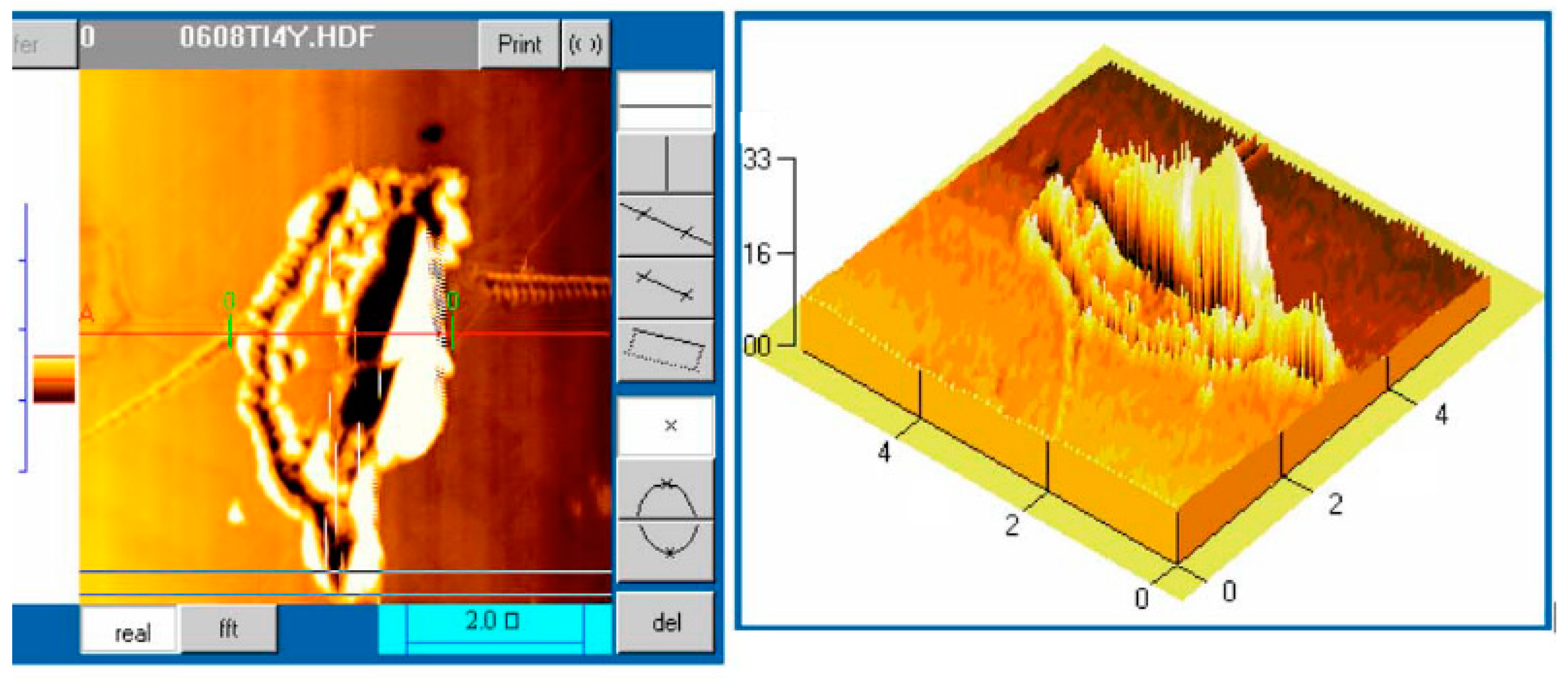
- Wang, J.; Yan, Y.; Li, Z.; Geng, Y.; Luo, X.; Fan, P. Processing outcomes of atomic force microscope tip-based nanomilling with different trajectories on single-crystal silicon. Precis. Eng. 2021, 72, 480–490. [Google Scholar] [CrossRef]
- Wang, J.; Geng, Y.; Li, Z.; Yan, Y.; Luo, X.; Fan, P. Study on the Vertical Ultrasonic Vibration-Assisted Nanomachining Process on Single-Crystal Silicon. J. Manuf. Sci. Eng. 2022, 144, 041013. [Google Scholar] [CrossRef]
- Xiao, G.; He, Y.; Geng, Y.; Yan, Y.; Ren, M. Molecular dynamics and experimental study on comparison between static and dynamic ploughing lithography of single crystal copper. Appl. Surf. Sci. 2019, 463, 96–104. [Google Scholar] [CrossRef]
- da Yan, Y.; Dong, S.; Sun, T. Investigation on Influencing Factors of AFM Micro Probe Nanomachining. In Materials Science Forum; Trans Tech Publications Ltd.: Zurich, Switzerland, 2004; Volume 471, pp. 816–820. [Google Scholar]
- Wang, J.; Yan, Y.; Jia, B.; Geng, Y. Study on the processing outcomes of the atomic force microscopy tip-based nanoscratching on GaAs. J. Manuf. Process. 2021, 70, 238–247. [Google Scholar] [CrossRef]
- Hyon, C.K.; Choi, S.C.; Hwang, S.W.; Ahn, D.; Kim, Y.; Kim, E.K. Direct nanometer-scale patterning by the cantilever oscillation of an atomic force microscope. Appl. Phys. Lett. 1999, 75, 292–294. [Google Scholar] [CrossRef]
- Wendel, M.; Kühn, S.; Lorenz, H.; Kotthaus, J.P.; Holland, M. Nanolithography with an atomic force microscope for integrated fabrication of quantum electronic devices. Appl. Phys. Lett. 1994, 65, 1775–1777. [Google Scholar] [CrossRef]
- Schumacher, H.W.; Keyser, U.F.; Zeitler, U.; Haug, R.J.; Eberl, K. Nanomachining of mesoscopic electronic devices using an atomic force microscope. Appl. Phys. Lett. 1999, 75, 1107–1109. [Google Scholar] [CrossRef]
- Bouchiat, V.; Esteve, D. Lift-off lithography using an atomic force microscope. Appl. Phys. Lett. 1996, 69, 3098–3100. [Google Scholar] [CrossRef]
- Lee, J.-M.; Jin, W.-H.; Kim, D.-E. Application of single asperity abrasion process for surface micro-machining. Wear 2001, 251, 1133–1143. [Google Scholar] [CrossRef]
- Lee, J.M.; Sung, I.H.; Kim, D.E. Process development of precision surface micro-machining using mechanical abrasion and chemical etching. Microsyst. Technol. 2002, 8, 419–426. [Google Scholar] [CrossRef]
- Yan, Y.; Sun, T.; Liang, Y.; Dong, S. Investigation on AFM-based micro/nano-CNC machining system. Int. J. Mach. Tools Manuf. 2007, 47, 1651–1659. [Google Scholar] [CrossRef]
- Yan, Y.; Hu, Z.; Zhao, X.; Sun, T.; Dong, S.; Li, X. Top-down nanomechanical machining of three-dimensional nanostructures by atomic force microscopy. Small 2010, 6, 724–728. [Google Scholar] [CrossRef] [PubMed]
- Mao, Y.-T.; Kuo, K.-C.; Tseng, C.-E.; Huang, J.-Y.; Lai, Y.-C.; Yen, J.-Y.; Lee, C.-K.; Chuang, W.-L. Research on three dimensional machining effects using atomic force microscope. Rev. Sci. Instrum. 2009, 80, 065105. [Google Scholar] [CrossRef] [PubMed]
- Sun, Y.; Yan, Y.; Hu, Z.; Zhao, X.; Yan, J. 3D polymer nanostructures fabrication by AFM tip-based single scanning with a harder cantilever. Tribol. Int. 2012, 47, 44–49. [Google Scholar] [CrossRef]
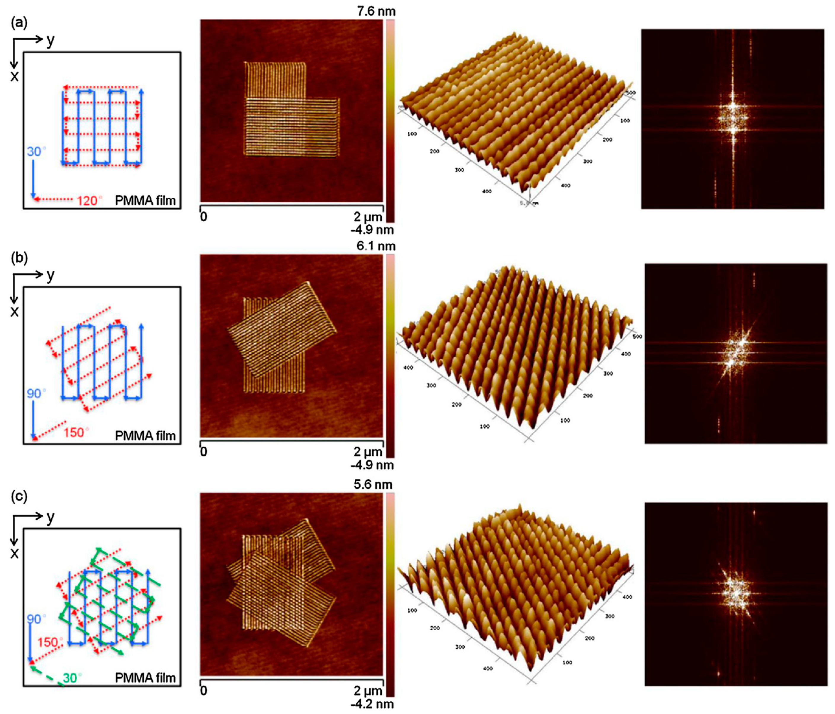
- He, Y.; Yan, Y.; Geng, Y.; Hu, Z. Fabrication of none-ridge nanogrooves with large-radius probe on PMMA thin-film using AFM tip-based dynamic plowing lithography approach. J. Manuf. Process. 2017, 29, 204–210. [Google Scholar] [CrossRef]
- He, Y.; Yan, Y.; Geng, Y.; Brousseau, E. Fabrication of periodic nanostructures using dynamic plowing lithography with the tip of an atomic force microscope. Appl. Surf. Sci. 2018, 427, 1076–1083. [Google Scholar] [CrossRef]
- Vasić, B.; Kratzer, M.; Matković, A.; Nevosad, A.; Ralević, U.; Jovanović, D.; Ganser, C. Atomic force microscopy based manipulation of graphene using dynamic plowing lithography. Nanotechnology 2013, 24, 015303. [Google Scholar] [CrossRef]
- Yan, Y.; He, Y.; Xiao, G.; Geng, Y.; Ren, M. Effects of diamond tip orientation on the dynamic ploughing lithography of single crystal copper. Precis. Eng. 2019, 57, 127–136. [Google Scholar] [CrossRef]
- Taha, H.; Marks, R.; Gheber, L.A.; Rousso, I.; Newman, J.; Sukenik, C.; Lewis, A. Protein printing with an atomic force sensing nanofountainpen. Appl. Phys. Lett. 2003, 83, 1041–1043. [Google Scholar] [CrossRef]
- Deng, J.; Zhang, L.; Dong, J.; Cohen, P.H. AFM-based 3D Nanofabrication Using Ultrasonic Vibration Assisted Nanomachining. Procedia Manuf. 2015, 1, 584–592. [Google Scholar] [CrossRef]
- Deng, J.; Dong, J.; Cohen, P. High Rate 3D Nanofabrication by AFM-based Ultrasonic Vibration Assisted Nanomachining. Procedia Manuf. 2016, 5, 1283–1294. [Google Scholar] [CrossRef]
- Kaestner, M.; Hofer, M.; Rangelow, I.W. Nanolithography by scanning probes on calixarene molecular glass resist using mix-and-match lithography. J. Micro/Nanolithogr. MEMS MOEMS 2013, 12, 031111. [Google Scholar] [CrossRef]
- Gartside, J.C.; Arroo, D.M.; Burn, D.M.; Bemmer, V.; Moskalenko, A.; Cohen, L.F.; Branford, W.R. Realization of ground state in artificial kagome spin ice via topological defect-driven magnetic writing. Nat. Nanotechnol. 2018, 13, 53–58. [Google Scholar] [CrossRef]
- Holz, M.; Allen, F.I.; Reuter, C.; Ahmad, A.; Hofmann, M.; Reum, A.; Ivanov, T.; Rangelow, I.W. Tip-based electron beam induced deposition using active cantilevers. J. Vac. Sci. Technol. B 2019, 37, 061812. [Google Scholar] [CrossRef]
- Bonthuis, D.J.; Meyer, C.; Stein, D.; Dekker, C. Conformation and dynamics of DNA confined in slitlike nanofluidic channels. Phys. Rev. Lett. 2008, 101, 2–5. [Google Scholar] [CrossRef]
- Cipriany, B.R.; Zhao, R.; Murphy, P.J.; Levy, S.L.; Tan, C.P.; Craighead, H.G.; Soloway, P.D. Single molecule epigenetic analysis in a nanofluidic channel. Anal. Chem. 2010, 82, 2480–2487. [Google Scholar] [CrossRef]
- Hu, H.; Zhuo, Y.; Oruc, M.E.; Cunningham, B.T.; King, W.P. Nanofluidic channels of arbitrary shapes fabricated by tip-based nanofabrication. Nanotechnology 2014, 25, 455301. [Google Scholar] [CrossRef]
- Iturri, J.; Toca-Herrera, J.L. Characterization of cell scaffolds by atomic force microscopy. Polymers 2017, 9, 383. [Google Scholar] [CrossRef]
- Marrese, M.; Guarino, V.; Ambrosio, L. Atomic Force Microscopy: A Powerful Tool to Address Scaffold Design in Tissue Engineering. J. Funct. Biomater. 2017, 8, 7. [Google Scholar] [CrossRef] [PubMed]
- SR, J.; Olusanya, T.O.B.; Lamprou, D.A. Characterization of drug delivery vehicles using atomic force microscopy: Current status. Expert Opin. Drug Deliv. 2018, 15, 1211–1221. [Google Scholar]
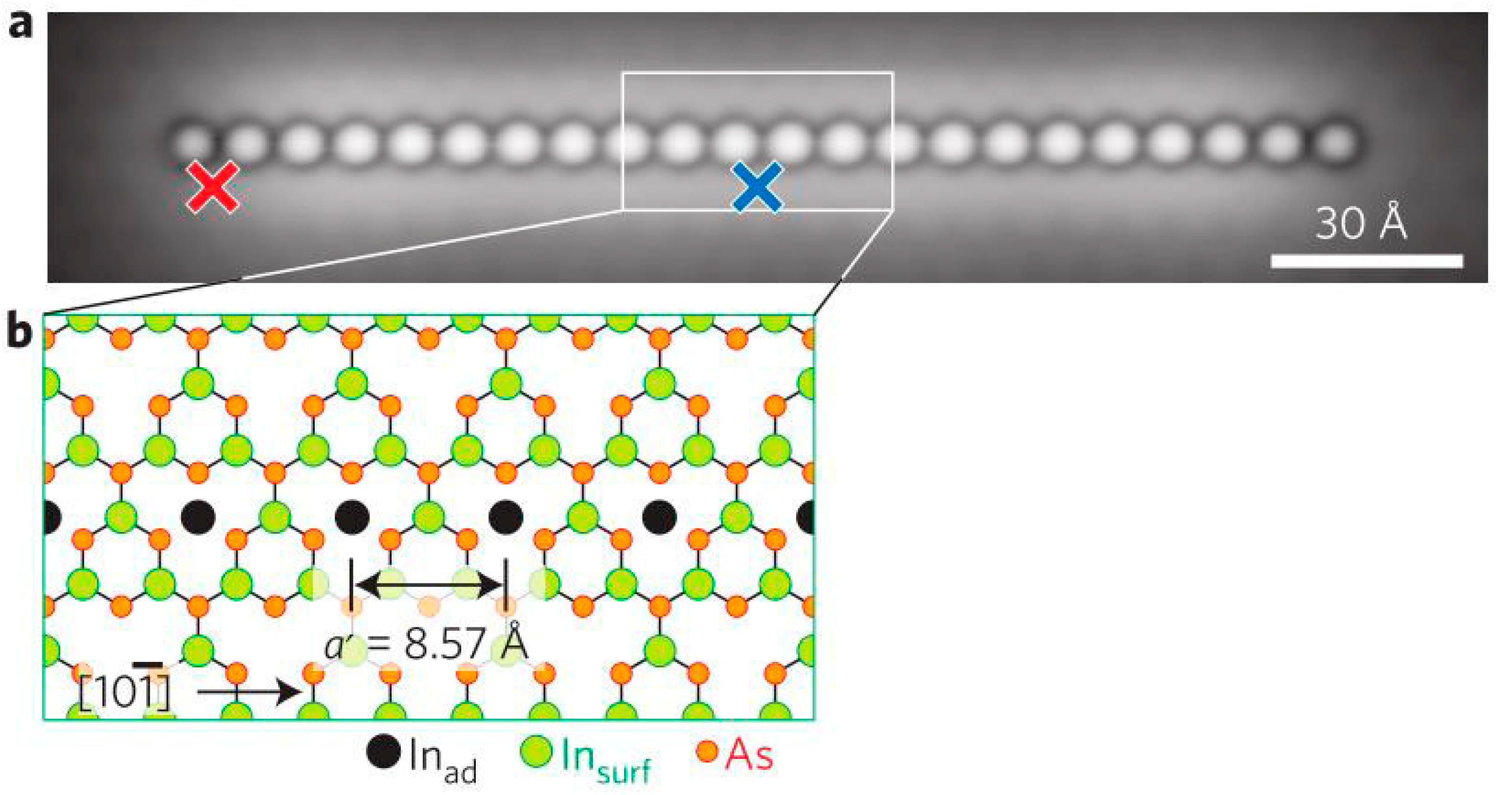
- Fölsch, S.; Martínez-Blanco, J.; Yang, J.; Kanisawa, K.; Erwin, S.C. Quantum dots with single-atom precision. Nat. Nanotechnol. 2014, 9, 505–508. [Google Scholar] [CrossRef] [PubMed]
- Hirjibehedin, C.F.; Lin, C.-Y.; Otte, A.F.; Ternes, M.; Lutz, C.P.; Jones, B.A.; Heinrich, A.J. Large Magnetic Anisotropy of a Single Atomic Spin Embedded in a Surface Molecular Network. Science 2007, 317, 1199–1203. [Google Scholar] [CrossRef]
- Lanza, M.; Wong, H.-S.P.; Pop, E.; Ielmini, D.; Strukov, D.; Regan, B.C.; Larcher, L.; Villena, M.A.; Yang, J.J.; Goux, L.; et al. Recommended Methods to Study Resistive Switching Devices. Adv. Electron. Mater. 2019, 5, 1800143. [Google Scholar] [CrossRef]
- Vuillaume, D. Molecular Electronics: From Single-Molecule to Large-Area Devices. Chempluschem 2019, 84, 1215–1221. [Google Scholar] [CrossRef]
- Durrani, Z.A.K.; Jones, M.E.; Wang, C.; Liu, D.; Griffiths, J. Excited states and quantum confinement in room temperature few nanometre scale silicon single electron transistors. Nanotechnology 2017, 28, 125208. [Google Scholar] [CrossRef]
- Durrani, Z.; Jones, M.; Abualnaja, F.; Wang, C.; Kaestner, M.; Lenk, S.; Lenk, C.; Rangelow, I.W.; Andreev, A. Room-temperature single dopant atom quantum dot transistors in silicon, formed by field-emission scanning probe lithography. J. Appl. Phys. 2018, 124, 144502. [Google Scholar] [CrossRef]
- Tseng, A.A. Three-dimensional patterning of nanostructures using atomic force microscopes. J. Vac. Sci. Technol. B Nanotechnol. Microelectron. Mater. Process. Meas. Phenom. 2011, 29, 040801. [Google Scholar] [CrossRef]
- Utada, K.; Ishida, K.; Nakamura, M.; Morimoto, Y.; Yamashita, S.; Sakabe, T. Nanofabrication by scanning probe microscope lithography: A review. J. Vac. Sci. Technol. B 2005, 53, 1396–1403. [Google Scholar]
- Tseng, A.A. Removing material using atomic force microscopy with single-and multiple-tip sources. Small 2011, 7, 3409–3427. [Google Scholar] [CrossRef] [PubMed]
- IRangelow, I.W.; Ivanov, T.; Ahmad, A.; Kaestner, M.; Lenk, C.; Bozchalooi, I.S.; Xia, F.; Youcef-Toumi, K.; Holz, M.; Reum, A. Review Article: Active scanning probes: A versatile toolkit for fast imaging and emerging nanofabrication. J. Vac. Sci. Technol. B Nanotechnol. Microelectron. Mater. Process. Meas. Phenom. 2017, 35, 06G101. [Google Scholar]
- Soukiassian, L.; Mayne, A.J.; Carbone, M.; Dujardin, G. Atomic wire fabrication by STM induced hydrogen desorption. Surf. Sci. 2003, 528, 121–126. [Google Scholar] [CrossRef]
- Paul, P.C.; Knoll, A.W.; Holzner, F.; Despont, M.; Duerig, U. Rapid turnaround scanning probe nanolithography. Nanotechnology 2011, 22, 275306. [Google Scholar] [CrossRef] [PubMed]
- Piner, R.D.; Zhu, J.; Xu, F.; Hong, S.; Mirkin, A.C. ‘Dip-Pen’ Nanolithography. Science 1999, 283, 661–663. [Google Scholar] [CrossRef] [PubMed]
- Anggraini, L.; Tanaka, B.; Matsuzuka, N.; Isono, Y. Scanning probe lithography with negative and positive electron beam resists. Jpn. J. Appl. Phys. 2013, 52, 056501. [Google Scholar] [CrossRef]
- Wang, J.; Zhang, Q.; Yan, Y.; Liu, Y.; Geng, Y. Fabrication of periodic nanostructures for SERS substrates using multi-tip probe-based nanomachining approach. Appl. Surf. Sci. 2022, 576, 151790. [Google Scholar] [CrossRef]
- Wang, Y.; Fan, P.; Luo, X.; Geng, Y.; Goel, S.; Wu, W.; Li, G.; Yan, Y. Fabrication of three-dimensional sin-shaped ripples using a multi-tip diamond tool based on the force modulation approach. J. Manuf. Process. 2021, 72, 262–273. [Google Scholar] [CrossRef]
- Gao, J.; Luo, X.; Fang, F.; Sun, J. Fundamentals of atomic and close-to-atomic scale manufacturing: A review. Int. J. Extrem. Manuf. 2022, 4, 012001. [Google Scholar] [CrossRef]


| Items | EBL | FIB | NIL | SPL |
|---|---|---|---|---|
| Principle | Physical process | Physical process | Physical and chemical process | Physical and chemical process |
| Machining capability | 2D, 3D | 2D, 3D | 2D, 2.5D | 2D, 3D |
| Resolution (nm) | 5 nm [7] | 5 nm [8] | 10 nm [9] | See Table 2 in Section 5 |
| Environmental conditions | Vacuum | Vacuum | Vacuum or ambient | Vacuum or ambient |
| Lithography speed | Slow 17 nm/min [10], 40 nm/min [11], and 58 nm/min [12] against different resists | Slow 0.05 μm3/s in FIB deposition [13] | Fast 15 wafers/h per imprint station [14] | See Table 2 in Section 5 |
| Cost | Higher start-up cost | Higher start-up cost | Low | Low |
| Contaminated patterns | Yes | Yes | No | No |
| Items | Close-to-Atomic Scale SPL | T/tc-SPL | O-SPL | M-SPL | D-SPL | B-SPL |
|---|---|---|---|---|---|---|
| Resolution | Atomic scale [3] | 10 nm [85] | 4 nm [60] | 10 nm [165] | 10 nm [74] | 10 nm [166] |
| Throughput | - | ~104 μm2 h−1 [167] | ~102 μm2 h−1 [66] | ~2.4 × 103 μm2 h−1 [112] | ~104 μm2 h−1 [98] | ~10 μm2 h−1 [168] |
| Machining capability | - | 2D, 3D | 2D, 3D | 2D, 3D | 2D | 2D |
| Machinable materials | Molecular, atoms, electrons | PMMA, PC PPV film, copolymer film | Metal, semiconductors, graphene, polymer | Polymer, metal, ceramics and semiconductors, graphene | Transporting organic molecules, polymers, DNA, proteins and metal ions | Graphene, metal, semiconductors, Si, polymer |
| Environmental conditions | Vacuum | Liquid, Air | 20%–80% relative humidity | Air | 34% relative humidity | High electric fields |
| Processing speed | Super slow 80 nm/s [169] | Super fast 20 mm/s [170] | Moderate 10 μm/s [74] | Fast 50 μm/s [2] | Slow 2 μm/s [171] | Slow 0.1 μm/s [172] |
| Control | Difficult | Good | Excellent | Excellent | Complicated | Difficult |
| Principle | Physico-chemistry process | Physico-chemistry process | Chemical process | Physical process | Chemical process | Physico-chemistry process |
| Tip wear | Negligible | Not serious | Negligible | Serious | Negligible | Negligible |
| Advantages | Atomic-scale precision | Super fast | Robust oxide formation | Easy to implement and various substrates materials | Very suitable for biological materials | Negligible probe wear |
| Disadvantages | Extreme slow | Requires heated probes | Requires oxidizability of the workpiece | Probe wear and burr formation | Requires ink | Requires extra electric circuits to control current |
Publisher’s Note: MDPI stays neutral with regard to jurisdictional claims in published maps and institutional affiliations. |
© 2022 by the authors. Licensee MDPI, Basel, Switzerland. This article is an open access article distributed under the terms and conditions of the Creative Commons Attribution (CC BY) license (https://creativecommons.org/licenses/by/4.0/).
Share and Cite
Fan, P.; Gao, J.; Mao, H.; Geng, Y.; Yan, Y.; Wang, Y.; Goel, S.; Luo, X. Scanning Probe Lithography: State-of-the-Art and Future Perspectives. Micromachines 2022, 13, 228. https://doi.org/10.3390/mi13020228
Fan P, Gao J, Mao H, Geng Y, Yan Y, Wang Y, Goel S, Luo X. Scanning Probe Lithography: State-of-the-Art and Future Perspectives. Micromachines. 2022; 13(2):228. https://doi.org/10.3390/mi13020228
Chicago/Turabian StyleFan, Pengfei, Jian Gao, Hui Mao, Yanquan Geng, Yongda Yan, Yuzhang Wang, Saurav Goel, and Xichun Luo. 2022. "Scanning Probe Lithography: State-of-the-Art and Future Perspectives" Micromachines 13, no. 2: 228. https://doi.org/10.3390/mi13020228
APA StyleFan, P., Gao, J., Mao, H., Geng, Y., Yan, Y., Wang, Y., Goel, S., & Luo, X. (2022). Scanning Probe Lithography: State-of-the-Art and Future Perspectives. Micromachines, 13(2), 228. https://doi.org/10.3390/mi13020228