
A Novel Memristive Neural Network Circuit and Its Application in Character Recognition


 ,
, 
Abstract
1. Introduction
2. Design of Memristive Synapse Circuit
2.1. Memristor Model
2.2. Weighted Operation
2.3. Weight Programming Operation
3. The Neuron Circuit
3.1. The Neuron Circuit Design
3.2. Simulation Analysis
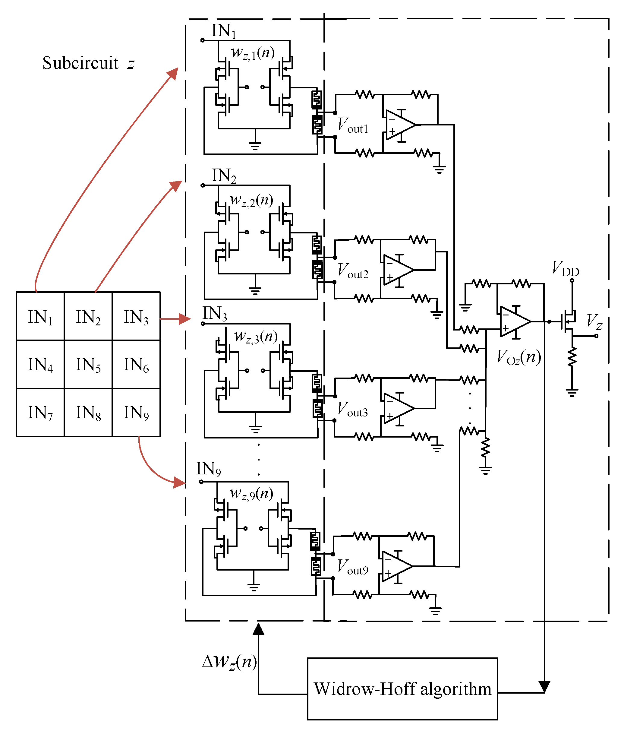
4. Circuit Implementation of the Character Recognition Network
5. Conclusions
Author Contributions
Funding
Institutional Review Board Statement
Informed Consent Statement
Data Availability Statement
Conflicts of Interest
References
- Xu, W.; Wang, J.; Yan, X. Advances in memristor-based neural networks. Front. Neurosci. 2021, 3, 645995. [Google Scholar] [CrossRef]
- Zhang, X.; Lu, J.; Wang, Z.; Rui, W. Hybrid memristor-CMOS neurons for in-situ learning in fully hardware memristive spiking neural networks. Sci. Bull. 2021, 66, 1624–1633. [Google Scholar] [CrossRef]
- Strukov, D.; Snider, G.; Stewart, D.; Williams, R. The missing memristor found. Nature 2008, 453, 80–83. [Google Scholar] [CrossRef]
- Hairong, L.; Chunhua, W.; Cong, X.; Xin, Z.; Herbert, H.C.; Iu, H.H. A Memristive Synapse Control Method to Generate Diversified Multi-Structure Chaotic Attractors. IEEE Trans. Comput.-Aided Des. Integr. Circuits Syst. 2022. [Google Scholar] [CrossRef]
- Cong, X.; Chunhua, W.; Jinguang, J.; Jingru, S.; Hairong, L. Memristive Circuit Implementation of Context-Dependent Emotional Learning Network and Its Application in Multi-Task. IEEE Trans. Comput.-Aided Des. Integr. Circuits Syst. 2022, 41, 3052–3065. [Google Scholar] [CrossRef]
- Leimin, W.; Zhigang, Z.; Ge, M.F. A disturbance rejection framework for finite-time and fixed-time stabilization of delayed memristive neural networks. IEEE Trans. Syst. Man Cybern. Syst. 2021, 51, 905–915. [Google Scholar] [CrossRef]
- Leimin, W.; Haibo, H.; Zhigang, Z. Global synchronization of fuzzy memristive neural networks with discrete and distributed delays. IEEE Trans. Fuzzy Syst. 2020, 28, 2022–2034. [Google Scholar] [CrossRef]
- Junwei, S.; Gaoyang, H.; Zhigang, Z.; Yangfeng, W. Memristor-based neural network circuit of full-function pavlov associative memory with time delay and variable learning rate. IEEE Trans. Cybern. 2019, 50, 2935–2945. [Google Scholar] [CrossRef]
- Junwei, S.; Juntao, H.; Yanfeng, W.; Peng, L. Memristor-based neural network circuit of emotion congruent memory with mental fatigue and emotion inhibition. IEEE Trans. Biomed. Circ. Syst. 2021, 15, 606–616. [Google Scholar] [CrossRef]
- Huang, L.; Diao, J.; Nie, H. Memristor based binary convolutional neural network architecture with configurable neurons. Front. Neurosci. 2021, 15, 639526. [Google Scholar] [CrossRef]
- Yang, X.; Taylor, B.; Wu, A. Research progress on memristor: From synapses to computing systems. IEEE Trans. Circuits Syst. I-Regul. Pap. 2022, 69, 1845–1857. [Google Scholar] [CrossRef]
- Hong, Q.; Zhao, L.; Wang, X. Novel circuit designs of memristor synapse and neuron. Neurocomputing 2019, 330, 11–16. [Google Scholar] [CrossRef]
- Ascione, F.; Bianco, N.; Stasio, C.D. Artificial neural networks to predict energy performance and retrofit scenarios for any member of a building category: A novel approach. Energy 2017, 118, 999–1017. [Google Scholar] [CrossRef]
- Moussa, H.G.; Husseini, G.A.; Abel-Jabbar, N. Use of model predictive control and artificial neural networks to optimize the ultrasonic release of a model drug from liposomes. IEEE Trans. Nanobiosci. 2017, 16, 149–156. [Google Scholar] [CrossRef] [PubMed]
- Del Campo, I.; Echanobe, J.; Bosque, G. Efficient hardware/software Implementation of an adaptive neuro-fuzzy system. IEEE Trans. Fuzzy Syst. 2008, 16, 761–778. [Google Scholar] [CrossRef]
- Draghici, S. Neural networks in analog hardware—Design and implementation issues. Int. J. Neural Syst. 2000, 10, 19–42. [Google Scholar] [CrossRef]
- Wei, F.; Chen, G.; Wang, W. Finite-time synchronization of memristor neural networks via interval matrix method. Neural Netw. 2020, 127, 7–18. [Google Scholar] [CrossRef]
- Adhikari, S.P.; Yang, C.; Kim, H.; Chua, L. Memristor bridge synapse-based neural network and its learning. IEEE Trans. Neural Netw. Learn. Syst. 2012, 23, 1426–1435. [Google Scholar] [CrossRef]
- Adhikari, S.P.; Kim, H.; Budhathoki, R.K. A circuit-based learning architecture for multilayer neural networks with memristor bridge synapses. IEEE Trans. Circuits Syst. I-Regul. Pap. 2014, 62, 215–223. [Google Scholar] [CrossRef]
- Prezioso, M.F.; Merrikh-Bayat, B.; Hoskins, D. Training and operation of an integrated neuromorphic network based on metal-oxide memristors. Nature 2015, 521, 61–64. [Google Scholar] [CrossRef]
- Alibart, F.; Zamanidoost, E.; Strukov, D. Pattern classification by memristive crossbar circuits using exsitu and insitu training. Nat. Commun. 2013, 4, 2072. [Google Scholar] [CrossRef]
- Chabi, D.; Wang, Z.; Bennett, C. Ultrahigh density memristor neural crossbar for on-chip supervised learning. IEEE Trans. Nanotechnol. 2015, 14, 954–962. [Google Scholar] [CrossRef]
- Hasan, R.; Taha, T.M. Enabling back propagation training of memristor crossbar neuromorphic processors. In Proceedings of the 2014 International Joint Conference on Neural Networks, Beijing, China, 6–11 July 2014; pp. 6–10. [Google Scholar] [CrossRef]
- Hasan, R.T.; Taha, M.; Yakopcic, C. A fast training method for memristor crossbar based multi-layer neural networks. Analog Integr. Circuits Process. 2017, 93, 443–454. [Google Scholar] [CrossRef]
- Lee, S.; Kim, S.; Cho, K.; Kang, S.M.; Eshraghian, K. Complementary resistive switch-based smart sensor search engine. IEEE Sens. J. 2014, 14, 1639–1646. [Google Scholar] [CrossRef]
- Yang, J.; Wang, L.; Duan, S. An anti-series memristive synapse circuit design and its application. Sci. Sin. Inf. 2016, 46, 391–403. [Google Scholar]
- Dong, Z.; Lai, C.S.; He, Y. Hybrid dual-complementary metal–oxide–semiconductor/memristor synapse-based neural network with its applications in picture super-resolution. IET Circuits Devices Syst. 2019, 13, 1241–1248. [Google Scholar] [CrossRef]
- Yang, L.; Zeng, Z.; Shi, X. A memristor-based neural network circuit with synchronous weight adjustment. Neurocomputing 2019, 363, 114–124. [Google Scholar] [CrossRef]
- Kim, H.; Sah, M.P.; Yang, C. Neural synaptic weighting with a pulse-based memristor circuit. IEEE Trans. Circuits Syst. I-Regul. Pap. 2012, 59, 148–158. [Google Scholar] [CrossRef]
- Rai, V.K.; Sakthivel, R. Design of artificial neuron network with synapse utilizing hybrid CMOS transistors with memristor for low power applications. J. Circuits Syst. Comput. 2020, 29, 1–20. [Google Scholar] [CrossRef]
- Soudry, D.; Castro, D.D.; Gal, A.; Kolodny, A.; Kvatinsky, S. Memristor-based multilayer neural networks with online gradient descent training. IEEE Trans. Neural Netw. Learn. Syst. 2015, 26, 2408–2421. [Google Scholar] [CrossRef]
- Ganorkar, S.; Sharma, S.; Jain, A. Soft Computing Algorithms and Implementation on FPGA-A Review. In Proceedings of the International Conference on Smart Data Intelligence, Tiruchirappalli, India, 26 May 2021. [Google Scholar] [CrossRef]
- Ansari, M.; Fayyazi, A.; Kamal, M. OCTAN: An on-chip training algorithm for memristive neuromorphic circuits. IEEE Trans. Circuits Syst. I-Regul. Pap. 2019, 66, 4687–4698. [Google Scholar] [CrossRef]
- Xu, C.; Wang, C.; Sun, Y. Memristor-based neural network circuit with weighted sum simultaneous perturbation training and its applications. Neurocomputing 2021, 462, 581–590. [Google Scholar] [CrossRef]
- Bayat, F.M.; Prezioso, M.; Chakrabarti, B. Memristor-based perceptron classifier: Increasing complexity and coping with imperfect hardware. In Proceedings of the IEEE/ACM International Conference on Computer-Aided Design, Irvine, CA, USA, 13–16 November 2017; pp. 549–554. [Google Scholar] [CrossRef]


| Conditions | Control Voltage | Transistor State |
|---|---|---|
| 1 | VG > 0 | T2, T3 = On T1, T4 = Off |
| 2 | VG < 0 | T1, T4 = On T2, T3 = Off |
| [26] | [27] | [28] | [29] | [30] | This Work | |
|---|---|---|---|---|---|---|
| Input | Voltage | Voltage | Voltage | Current | Voltage | Voltage |
| Output | Voltage | Current | Current | Voltage | Current | Voltage |
| Weight scope | + | +, 0, − | +, 0, − | +, 0, − | + | +, 0, − |
| Weight linearity | Yes | Yes | No | No | No | Yes |
| Number of memristors | 2 | 2 | 1 | 5 | 1 | 2 |
| Number of control voltages | 1 | 2 | 2 | 2 | 1 | 1 |
| Stages | Time (ms) | Observation |
|---|---|---|
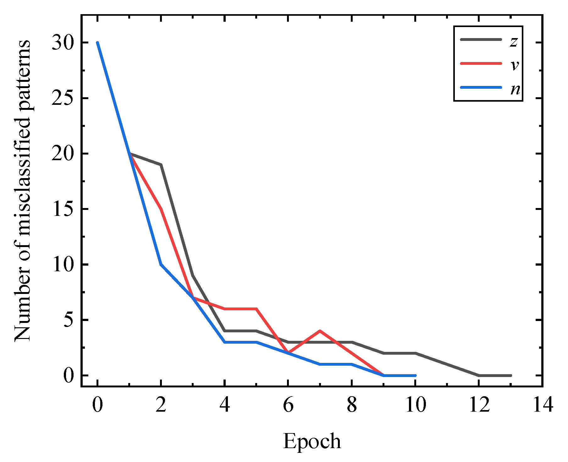
| I | 0–0.03 | Input three standard pictures of z, v, and n into the circuit in turn. |
| II | 0.03–0.05 | Continuously input the noisy pictures of each character into the circuit twice in turn |
| III | 0.09–0.12 | Continuously input the noisy pictures of each character into the circuit three times in turn |
| IV | 0.18–0.3 | Continuously input the noisy pictures of each character into the circuit four times in turn |
Publisher’s Note: MDPI stays neutral with regard to jurisdictional claims in published maps and institutional affiliations. |
© 2022 by the authors. Licensee MDPI, Basel, Switzerland. This article is an open access article distributed under the terms and conditions of the Creative Commons Attribution (CC BY) license (https://creativecommons.org/licenses/by/4.0/).
Share and Cite
Zhang, X.; Wang, X.; Ge, Z.; Li, Z.; Wu, M.; Borah, S. A Novel Memristive Neural Network Circuit and Its Application in Character Recognition. Micromachines 2022, 13, 2074. https://doi.org/10.3390/mi13122074
Zhang X, Wang X, Ge Z, Li Z, Wu M, Borah S. A Novel Memristive Neural Network Circuit and Its Application in Character Recognition. Micromachines. 2022; 13(12):2074. https://doi.org/10.3390/mi13122074
Chicago/Turabian StyleZhang, Xinrui, Xiaoyuan Wang, Zhenyu Ge, Zhilong Li, Mingyang Wu, and Shekharsuman Borah. 2022. "A Novel Memristive Neural Network Circuit and Its Application in Character Recognition" Micromachines 13, no. 12: 2074. https://doi.org/10.3390/mi13122074
APA StyleZhang, X., Wang, X., Ge, Z., Li, Z., Wu, M., & Borah, S. (2022). A Novel Memristive Neural Network Circuit and Its Application in Character Recognition. Micromachines, 13(12), 2074. https://doi.org/10.3390/mi13122074