Abstract
This paper introduces a compact SPICE model of a two-terminal memory with a Pd/Ti/IGZO/p+-Si structure. In this paper, short- and long-term components are systematically separated and applied in each model. Such separations are conducted by the applied bias and oxygen flow rate (OFR) during indium gallium zinc oxide (IGZO) deposition. The short- and long-term components in the potentiation and depression curves are modeled by considering the process (OFR of IGZO) and bias conditions. The compact SPICE model with the physical mechanism of SiO2 modulation is introduced, which can be useful for optimizing the specification of memristor devices.
1. Introduction
The Internet of Things (IoT) refers to a technology in which sensors are attached to objects to exchange data in real time over the Internet. Edge computing is used to reduce latency and bandwidth by performing computing at or near the physical location of a user or data source for IoT [1,2,3,4,5,6]. Due to the increasing variety of image sensing data, the demand for technology using IoT is increasing, and data collection and analysis technology must be specified. Memristor can be a building block in neuromorphic systems by controlling conductance [7,8,9,10,11,12,13]. Various resistive switching behaviors are observed in a lot of materials, such as oxides, nitrides and other materials [14,15,16,17,18,19,20,21,22]. Among them, the indium gallium zinc oxide (IGZO)-based memristor is very promising for memory applications because of its interface-type switching and good compatibility with conventional Si processing [14,15,16,17,18,19].
In previous studies, IGZO-based memristors have shown good synaptic properties for neuromorphic systems and memory applications [14,15,16,17,18,19,20,21]. Similarly to other oxide memristors, when Ag is used as the top electrode (TE) in IGZO-based memristors, Ag plays a dominant role in switching through the formation of the Ag filament [22,23,24]. Conversely, intrinsic resistive switching was observed when non-chemical metallization memory-type electrodes were used [25]. Here, in most cases, a gradual change in resistance is observed, indicating that the interface of the IGZO and electrode layers plays an important role in the resistance change. Non-filamentary switching, as observed in several material systems, provides better conductance control for neuromorphic system [26,27,28].
Basically, good long-term memory retention is beneficial for the neuromorphic system to ensure good performance without data loss [29,30]. Meanwhile, short-term memory with resistance drift is rather suitable for temporal learning which could save the leaning cost in reservoir computing [28]. Therefore, the distinction between the short- and long-term components in the memristor could be important. However, in previous studies, the classification of short- and long-term components has rarely been reported [31]. In our previous papers, we characterized the resistive switching and synaptic characteristics of a IGZO/SiO2/Si structure that is compatible with CMOS [14,15,16,17,18]. This paper introduces the compact SPICE model of a two-terminal memory with a Pd/Ti/IGZO/p+-Si structure in which the Si bottom electrode (BE) is favorable to a CMOS process [32,33]. The short- and long-term components are systematically separated and analyzed in each model. We proceeded with the separation of the short- and long-term components by applying bias to the samples with different oxygen flow rates (OFRs) during IGZO deposition. The compact SPICE model introduced in this paper can be used to optimize the specifications of the memristor.
2. Experimental Section
An initial cleaning of the p-type Si wafer with a boron doping concentration of 2 × 1019 cm−3 was conducted for the Pd/IGZO/SiO2/p+-Si memristors. The p-type Si wafer acts as the BE of the memristor system. A 60 nm-thick IGZO film was deposited at a power of 150 W using a radio-frequency (RF) sputtering system. The Ar flow was 3 sccm and the O2 flow rates (OFR) were 1, 1.5 and 2 sccm for the three samples, respectively. A SiO2 layer was formed as a native oxide between the p+-Si and IGZO layers [15]. Then, a 2 nm-thick Ti layer and a 40 nm-thick Pd layer were deposited by e-beam evaporation as an adhesion layer and a top electrode (TE). In addition, Ti and Pd patterning was carried out using a shadow mask with a rectangular pattern measuring 100 μm × 400 μm.
3. Results and Discussion
The typical characteristics of the memristor used in this work are as follows. When a strong negative voltage is applied to the TE, oxygen vacancies (V02+) inside the IGZO film are driven toward the TE and the filament composed of V02+ is formed, which extends from the TE to the BE for the formation process, as shown in Figure 1a,b. After the formation process, the Schottky barrier on the TE side collapses, and the barrier formed by the SiO2 layer on the BE side is modulated, resulting in the memristor switching characteristics [15,34]. The barrier height (BH) of SiO2 is modulated by electron trapping/detrapping in the trap at the interface between the IGZO and SiO2 layers. When a positive voltage is applied to the TE, the electrons are detrapped in the trap at the IGZO–SiO2 interface, causing a relatively positive charge. The BH is lowered and the memristor resistance decreases for the SET process in Figure 1c. Conversely, when a negative voltage is applied to TE, electrons are detrapped in the trap at the IGZO and SiO2 interface, resulting in a relatively negative charge, and the BH increases, thereby increasing the resistance of the memristor for the RESET process shown in Figure 1d.
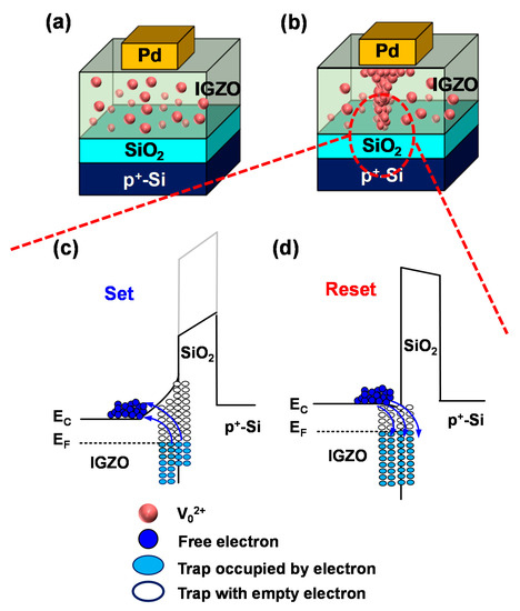
Figure 1.
Device stacks of Pd/IGZO/SiO2/p+-Si memristors for (a) HRS and (b) LRS. Energy band diagram of the Pd/IGZO/SiO2/p+-Si memristors for (c) HRS and (d) LRS.
The main current mechanism of the memristor is the thermionic emission of the barrier formed by native oxide [15,18,31]. The current formula by thermionic emission is the same as Equation (1):
where A is the device area; A* is the Richardson constant; T is the absolute temperature; k is the Boltzmann constant; VTE is the voltage applied to TE; q is the electric charge; εSiO2 is the dielectric constant at SiO2; Leff is the native oxide effective thickness; and Φ(t) is the native oxide effective BH [12]. The barrier modulation by the memristor switching operation drops from the initial BH (Φinit(t)) to the BH change amount (ΔΦ(t)) in Equation (2).
ΔΦ(t) is calculated by Equation (3) for potentiation and Equation (4) for depression [12].
Equations (3) and (4) are double-stretched exponential functions (DSEFs) composed of two sums of stretched exponential functions, and each stretched exponential function (SEF) is responsible for the modulation of the barrier during short- and long-term operations. ΔΦS(t) and ΔΦL(t) are the total amount of change of the current BH by the short- and long-term components, respectively.
ΔΦS0, ΔΦL0, τpS, τpL, τdS, τdL, βpS, βpL, βdS and βdL are all fitting parameters that form the DSEF [12]. ΔΦS0, ΔΦL0, τpL, τdL and βpL are expressed as functions of the externally applied bias and OFR. The parameter extraction process will be described later.
To extract the parameters that constitute the DSEF from Equation (3), an experimental sequence was designed as shown in Figure 2a. Conduct the potentiation and recovery experiments simultaneously. Separate the ΔΦS by fitting from the recovery test result. Fit the ΔΦL component from the potentiation test result. If the above steps are performed for each potentiation voltage (VP), the DSEF parameter can be expressed as a function of VP for the device with 2 sccm.
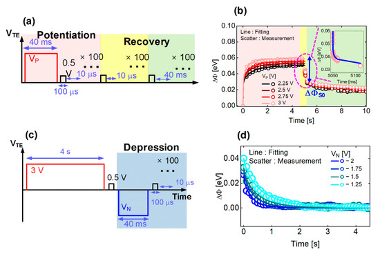
Figure 2.
Potentiation and recovery pulse sequence to extract the DSEF modeling parameters. (a) Schematic of the potentiation and recovery pulse sequence (b) Potentiation and recovery curves when applying different Vp: the red, yellow and green regions indicate potentiation, short-term component and long-term component of the recovery phase, respectively. (c) Pulse sequences to extract the long-term SEF parameter. (d) Extraction of τdL and βdL using the long-term component fitting line.
First, a stress pulse of magnitude VP was applied to TE for 40 ms, and then a read pulse was applied for 100 μs with an interval time of 10 μs. The current was measured while applying the read pulse to observe the change in the memristor conductance at every potentiation pulse. The read operation period was 120 μs in total, including the state in which no pulse was applied. It was very short considering that the potentiation pulse width was 40 ms. The reason for this design was that the read process is performed for the shortest time possible so as not to lose the data of the short-term component during the read operation. According to the above procedure, the potentiation and read pulses are applied continuously, and this is repeated 100 times to end the potentiation phase in the red box region of Figure 2a. Once the potentiation phase is completed, we move to the recovery phase, which consists of two phases: the yellow and green regions in Figure 2a. The yellow box was designed with a tight read pulse interval of 10 μs to observe the recovery by the short-term component.
In Figure 2a, the green box is designed with a read pulse interval of 40 ms duration to see the recovery by the long-term component. In each recovery phase, 100 read pulses are applied.
The above experiment was repeated by dividing it into four cases of VP = 2.25, 2.5, 2.75 and 3 V.
Figure 2b shows the results measured by the procedure proposed in Figure 2a. The current measured while applying the read pulse was converted to Φ by Equation (1), and ΔΦ was calculated through Equation (2). The results of the potentiation phase are expressed in the red region, and the results of the short- and long-term recovery phases are expressed in the yellow region and the green box, respectively.
First, as indicated by the blue arrow in Figure 2b, the decrease in ΔΦ with a steep slope was regarded as the barrier change due to the short-term component that was defined as ΔΦS0. ΔΦS0 is extracted for each VP and can be expressed as a bias function (Equation (6)). Second, τpS and βpS are extracted by fitting short-term components, as shown in the inset of Figure 2b. Here, two assumptions are made about the short-term component. The first assumption is that τdS = τpS and βdS = βpS. The second assumption is that τdS and βdS are independent of bias and OFR. The change in BH of the short-term component proceeds at least 200 times faster than that of the long-term component. Therefore, it is very difficult to detect the τ and β trend of the short-term component by the bias or process conditions; therefore, the above assumption was made. Third, ΔΦL0, τpL, and βpL are extracted by fitting while fixing ΔΦS0, τpS and βpS in the red region of Figure 2b with Equation (3). Repeating for each VP, ΔΦL0 (Equation (5)), τpL (Equation (7)) and βpL can be expressed as a function of bias.
Then, we designed an experimental sequence as shown in Figure 2c to extract the long-term SEF parameter of Equation (4). First, we applied the potentiation pulse of 3 V to the TE for 4 s to sufficiently increase the conductance of the memristor, and then applied a depression pulse. For the depression phase, as shown in the blue box region in Figure 2c, a stress pulse with a magnitude of VN is applied for 40 ms, and then a read pulse is applied for 100 μs with an interval time of 10 μs. The depression and read pulses are continuously applied and this is repeated 100 times.
The result of the above experimental procedure is shown in Figure 2d, and as shown in Figure 2c, the current measured in the read pulse was converted to ΔΦ by Equations (1) and (2). The long-term SEF parameter extraction procedure of Equation (4) is as follows. τdL and βdL are extracted by fitting (line) the measurement data (scatter) as shown in Figure 2d, with the long-term part of Equation (4). By fitting the entire VN, the parameters τdL (Equation (8)) and βdL can be expressed as a function of the bias.
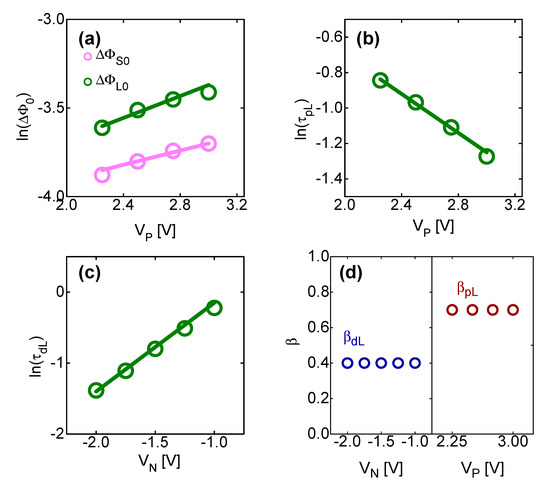
Figure 3.
(a) ΔΦS0 and ΔΦL0 as a function of VP; (b) τpL as a function of Vp; and (c) τdL as a function of VN. (d) βpL and βdL as a function of VN and VP, respectively.
ΔΦS0 and ΔΦL0 are the BH of the short- and long-term components that can be shifted to the maximum when VTE is VP. It was empirically verified that both ΔΦS0 and ΔΦL0 increase exponentially with respect to VP. Conversely, Figure 3b shows the experimentally revealed relationship between τpL and VP. τpL is a parameter related to the detrapping time of electrons by the long-term component in the potentiation. It was empirically found that ΦpL decreases exponentially with VP. The higher the voltage applied to TE, the lower the Fermi level at the SiO2–IGZO interface, so the concentration of traps where electrons can be detrapped increases. Therefore, the maximum changeable BH (ΔΦS0 and ΔΦL0) increases. Conversely, the probability that VP can cause electron detrapping at the SiO2–IGZO interface increases, so τpL (detrapping time) decreases.
Figure 3c shows the experimentally revealed relationship between VN and τdL. τdL is a parameter related to the electron trapping time by the long-term component in the depression. τdL was empirically found to increase exponentially with VN. As the voltage applied to the TE increases, the fermi level at the SiO2 and IGZO interface decreases, so the concentration of trap sites that can trap electrons decreases. Therefore, the time for trapping electrons increases.
Figure 3d shows the relationship between βpL, βdL, VP and VN. βpL and βdL are parameters that indicate the rate of change over time of τpL and τdL by long-term components during potentiation and depression, respectively. It was experimentally found that βpL and βdL are independent of the bias applied to the TE.
Then, when the parameter extraction process in Figure 2 proceeds for the sample with different OFRs, the DSEF parameter (Equations (3) and (4)) can be expressed as a function of the OFRs. Figure 4 shows the results of the experiments conducted for this purpose. Figure 4a shows the experiment results when the 2.5 V VP is fixed independently of the OFR in the pulse sequence of Figure 2a. The DSEF parameters (ΔΦS0, ΔΦL0, τpL and βpL) of Equation (3) were extracted for the different OFRs, and the extraction procedure is the same as that of the method shown in Figure 2b. Similarly, Figure 4b shows the experimental results when VN is −1.5 V regardless of the OFR in the pulse sequence of Figure 2c. The long-term SEF parameters (τdL and βdL) of Equation (4) were extracted for the samples with different OFRs by Figure 4b, and the extraction procedure is the same as that in Figure 2d.
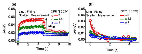
Figure 4.
(a) Measurement and fitting results of ΔΦ in different OFRs (1, 1.5 and 2 sccm) when applying the pulse sequence of Figure 2a with a VP of 2.5 V; and (b) Measurement and fitting results of ΔΦ in different OFRs (1, 1.5 and 2 sccm) when applying the pulse sequence of Figure 2c with a VN of −1.5 V.
Figure 5 shows the plots of the parameters with different OFRs for ΔΦS0, ΔΦL0, τpL, τdL, βpL, and βdL extracted from the measurement data of Figure 4. Figure 5a shows ΔΦS0 and ΔΦL0 as a function of OFR. Figure 5b,c shows τpL and τdL as a function of OFR. Figure 5d shows βpL and βdL as a function of OFR.
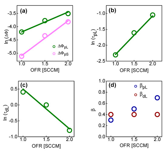
Figure 5.
(a) ΔΦpL and ΔΦpS as a function of OFR; (b) τpL as a function of OFR; and (c) τdL as a function of OFR. (d) βpL and βdL as a function of OFR.
It was experimentally found that ΔΦS0, ΔΦL0 and τpL increase exponentially with increasing OFR, but τpL decreases exponentially as OFR increases. As OFR increases, the traps between IGZO and SiO2 increase. There are two main reasons for this trend. The first is that the roughness of the IGZO–SiO2 interface increases and the trap concentration increases. This could be associated with the short-term component. The second is that, when the OFR increases, the bulk trap inside the IGZO increases because the oxygen peroxide inside the IGZO breaks bonds and acts as an electron trap. This could be related to the long-term component. The long-term switching mechanism could be caused by the charge change due to the reaction between oxygen peroxide and excess oxygen of the BE side IGZO. The excess oxygen is converted into oxygen peroxide for the SET process. Conversely, the oxygen peroxide in converted back into excess oxygen for the RESET process. Therefore, as OFR increases, the trap concentration near SiO2 increases; therefore, ΔΦS0 and ΔΦL0 increase.
During the potentiation operation, the resistance of the switching site in the SiO2 layer gradually decreases, so the actual voltage applied to SiO2 gradually decreases. This phenomenon has the effect of lowering τ by rapidly saturating the conductance change of the memristor. The lower the OFR, the more severe the phenomenon in which the voltage applied to the switching site gradually decreases during the potentiation operation. Therefore, the lower the OFR, the lower the τ.
Conversely, for the depression operation, the resistance of the switching site gradually increases, so the voltage actually applied to the SiO2 gradually increases. This has the effect of increasing τ as it can sustain the change in the conductance of the memristor. The lower the OFR, the higher the voltage applied to the switching place increases during the depression operation, which has the effect of increasing τ. Therefore, the lower the OFR, the higher the τ.
Although βpL increases with increasing OFR, βdL remains constant, however, the cause remains to be discussed further. Therefore, finally, by combining the results of Figure 3 and Figure 5, the correlation between the parameters (including ΔΦS0, ΔΦL0, τpL and τdL), the bias and OFR can be found. Among them, ΔΦS0, ΔΦL0, τpL and τdL are expressed in Equations (5)–(9).
Table 1 includes the initial parameters extracted by OFR. Leff is the effective SiO2 thickness that determines the thermionic emission. When a voltage is actually applied to the TE, the voltage is distributed between the IGZO and the SiO2, however, the current model is designed so that all voltages are applied to the SiO2. Therefore, the actual Leff of SiO2 is determined by the degree of voltage distribution between the IGZO and SiO2, and the model is designed so that all voltages are applied to SiO2 with a thickness of Leff. Leff decreases as the resistance of the IGZO decreases and that of SiO2 increases. The larger the OFR, the thicker the SiO2 (as the SiO2 resistance increases), and so the Leff decreases. Since the concentration of VO2+ in the IGZO increases as the OFR decreases, the IGZO becomes positively charged as a whole and the initial BH decreases.

Table 1.
Thermionic emission current parameters.
From the results of Figure 3 and Figure 5, the parameters αVL, αOL, αL, αVS, αOS, αS, γpVL, γpOL, γpL, γdVL, γdOL, γdL, κpL and κ can be determined (Table 2, lines 1–4). In addition, the parameters independent of OFR and bias are constant (Table 2, lines 5–8).
Table 2.
DSEFs parameters.
Figure 6 shows the algorithm of the compact memristor model designed with SPICE’s Verilog-A. The simulation proceeds in a time-transient manner, and Figure 6 schematically shows the calculated algorithm in one time step.
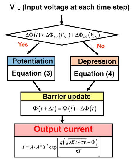
Figure 6.
Algorithm of the compact model designed with SPICE’s Verilog-A for the barrier-modulated memristor.
The input is the voltage and the output is the current composed by the thermionic emission formula [11]. Additionally, the size of BH is updated at each time step. The maximum value that BH can be modulated by the input voltage is (ΦL0(VTE) + ΦS0(VTE)). If (ΦL0(VTE) + ΦS0(VTE)) is greater than the current change in ΔΦ(t), potentiation is performed. If (ΦL0(VTE) + ΦS0(VTE)) is smaller than the current BH change in ΔΦ(t), depression is executed. This is because the BH must be lower. The potentiation is calculated by Equation (3), and the depression is calculated by Equation (4). If Φ is calculated every time step by the potentiation and depression operation, Φ is finally determined in the thermionic emission equation to calculate the current as output.
To verify that the memristor current mechanism is thermionic emission, the I–V curve in Figure 7a is presented as a relationship between ln(I) versus VTE1/2, and ln(I) and VTE1/2 show a linear relationship which was confirmed in Figure 7b. Here, as shown in Figure 7b, can be known by the slope of the HRS current line, and Leff can be extracted from this relationship. Moreover, by the point where V = 0, we can know that Φinit, and from it, we can extract Φinit. Figure 7a shows the I–V characteristics of memristors with different OFRs, and we compare the measurement and simulation results. The I–V curves of the memristors were applied to the TE in a double sweep in 0.1 V steps with the range of −5 V to 5 V, and the compliance current was set to 1 mA. Figure 7a shows that the measurement and simulation results are well matched.
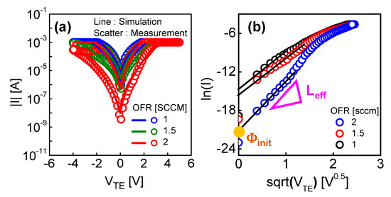
Figure 7.
(a) I–V curves and (b) ln(I) versus VTE1/2 the memristor devices with different OFR conditions (1, 1.5 and 2 sccm) to extract Φinit.
Figure 8 shows the potentiation and depression behaviors of the memristors with the different OFRs, and the experimental results and simulations were compared. The potentiation pulse had an amplitude of 3.5 V and a width of 30 ms, and a read pulse with an amplitude of 0.5 V and a width of 100 μs was applied with an interval of 100 μs. After repeating the potentiation pulse and the read pulse 50 times, a depression pulse was applied. The depression pulse was set at −1.5 V amplitude and 30 ms width, and a read pulse was applied under the same conditions as the potentiation. Similarly, the depression and read pulses were repeated 50 times and the experiment was completed. Figure 8b,c show the device results with 2 sccm and 1.5 sccm, respectively. Figure 8d shows the result of the device with 1 sccm, which has a good match. The memristor conductance was determined differently depending on the size and interval of the stimulation pulses. The stronger and longer the stimulus, the closer the memristor conductance is to long-term memory. Conversely, when the stimulus is weaker and shorter, the memristor conductance does not increase, and the conductance increases temporarily and then only decreases at the time of stimulation, acting close to short-term memory.
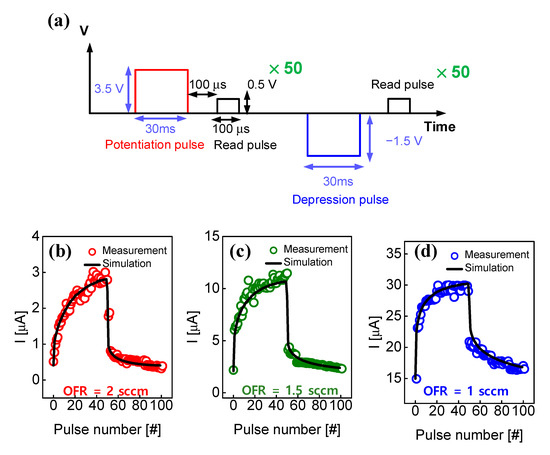
Figure 8.
(a) Pulse scheme for potentiation and depression. Potentiation and depression curves of measurement and simulation as a function of pulse number for devices with different OFRs: (b) 2 sccm, (c) 1.5 sccm and (d) 1 sccm.
In addition, the memristor model introduced in this paper can reproduce short- and long-term memory behaviors depending on the stimulation conditions. To confirm this, a pulse sequence was designed as shown in Figure 9a. The stimulation pulse is used to increase the conductance of the memristor, and the interval between each stimulation pulse is fixed at 100 ms. In addition, to observe the conductance change in detail up to the short-term component, a read pulse of 0.5 V amplitude β was applied at 0.4 ms intervals. Figure 9b shows the results of dividing the stimulation pulse width (twidth) into 0.1, 1, 4 and 40 ms while keeping the stimulation pulse amplitude (VSt) constant at 4 V. Figure 9c shows the results of dividing the stimulation pulse width (twidth) to 30 ms and the stimulation pulse amplitude (VSt) to 4.5, 4, 3.5 and 3 V. As the stimulus is delivered over a longer period of time, the conductance of the memristor gradually increases and operates close to the long-term memory, and the simulation reproduces the trend well.
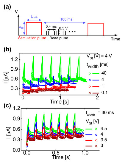
Figure 9.
(a) Pulse schemes including stimulation and read pulses to emulate short- and long-term memory characteristics. (b) Conductance change by controlling the pulse width (twidth) and (c) amplitude of the stimulated pulse (Vst).
4. Conclusions
This paper introduced a compact SPICE model of a two-terminal memory with a Pd/Ti/IGZO/p+-Si structure. The modeling of the SiO2 BH modulation related to the switching operation is the core of this work. We separated the BH modulation into short- and long-term components through potentiation, depression and recovery experiments with very tight pulse intervals. The empirical model for short- and long-term memory was designed by conducting the above experiment for the device with different OFR conditions when biasing. As the magnitude of the potentiation pulse and OFR increases, the maximum value of the BH modulation increases exponentially. Conversely, as the magnitude of the potentiation pulse increases, the potentiation speed increases; however, as the OFR increases, the potentiation speed decreases. As the amplitude of the depression pulse increases and the OFR increases, the depression rate increases. We expect that this model can be useful in optimizing the memristor specifications for short- and long-term memories.
Author Contributions
Conceptualization, D.K. and D.H.K.; formal analysis, H.J.L. and T.J.Y.; investigation, W.S.C.; methodology, C.K., S.-J.C., J.-H.B., D.M.K. and D.H.K.; writing—original draft D.K. and S.K.; writing—review and editing, D.H.K. and S.K. All authors have read and agreed to the published version of the manuscript.
Funding
This work was supported in part by the National Research Foundation of Korea (NRF) grant funded in part by the Korean Government (MSIT) (No. 2016R1A5A1012966 and No. 2020R1A2B5B01001979) by the Institute of Information and Communications Technology Planning and Evaluation (IITP) grant funded by the Korean government (MSIT) (No. 2021-0-01764) and by the Brain Korea 21 Four Program.
Institutional Review Board Statement
Not applicable.
Informed Consent Statement
Not applicable.
Data Availability Statement
Not applicable.
Conflicts of Interest
The authors declare no competing financial interests.
References
- Li, H.; Ota, K.; Dong, M. Learning IoT in Edge: Deep Learning for the Internet of Things with Edge Computing. IEEE Netw. 2018, 32, 96–101. [Google Scholar] [CrossRef]
- Hamdan, S.; Ayyash, M.; Almajali, S. Edge-Computing Architectures for Internet of Things Applications: A Survey. Sensors 2020, 20, 6441. [Google Scholar] [CrossRef] [PubMed]
- Capra, M.; Peloso, R.; Masera, G.; Roch, M.R.; Martina, M. Edge Computing: A Survey on the Hardware Requirements in the Internet of Things World. Future Internet 2019, 11, 100. [Google Scholar] [CrossRef]
- Chen, B.; Wan, J.; Celesti, A.; Li, D.; Abbas, H.; Zhang, Q. Edge Computing in IoT-Based Manufacturing. IEEE Commun. Mag. 2018, 56, 103–109. [Google Scholar] [CrossRef]
- Sittón-Candanedo, I.; Alonso, R.S.; García, Ó.; Muñoz, L.; Rodríguez-González, S. Edge Computing, Iot and Social Computing in Smart Energy Scenarios. Sensors 2019, 19, 3353. [Google Scholar] [CrossRef] [PubMed]
- Covi, E.; Donati, E.; Liang, X.; Kappel, D.; Heidari, H.; Payvand, M.; Wang, W. Adaptive Extreme Edge Computing for Wearable Devices. Front. Neurosci. 2021, 15, 611300. [Google Scholar] [CrossRef]
- Li, H.; Wang, S.; Zhang, X.; Wang, W.; Yang, R.; Sun, Z.; Feng, W.; Lin, P.; Wang, Z.; Sun, L.; et al. Memristive Crossbar Arrays for Storage and Computing Applications. Adv. Intell. Syst. 2021, 3, 2100017. [Google Scholar] [CrossRef]
- Wang, W.; Covi, E.; Milozzi, A.; Farronato, M.; Ricci, S.; Sbandati, C.; Pedretti, G.; Ielmini, D. Neuromorphic Motion Detection and Orientation Selectivity by Volatile Resistive Switching Memories. Adv. Intell. Syst. 2021, 3, 2000224. [Google Scholar] [CrossRef]
- Wang, W.; Song, W.; Yao, P.; Li, Y.; Nostrand, J.V.; Qiu, Q.; Ielmini, D.; Yang, J.J. Integration and Co-design of Memristive Devices and Algorithms for Artificial Intelligence. IScience 2020, 23, 101809. [Google Scholar] [CrossRef]
- Wang, C.; He, W.; Tong, Y.; Zhao, R. Investigation and Manipulation of Different Analog Behaviors of Memristor as Electronic Synapse for Neuromorphic Applications. Sci. Rep. 2016, 6, 22970. [Google Scholar] [CrossRef]
- Indiveri, G.; Linares-Barranco, B.; Legenstein, R.; Deligeorgis, G.; Prodromakis, T. Integration of Nanoscale Memristor Synapses in Neuromorphic Computing Architectures. Nanotechnology 2013, 24, 384010. [Google Scholar] [CrossRef] [PubMed]
- Thomas, A. Memristor-Based Neural Networks. J. Phys. D Appl. Phys. 2013, 46, 093001. [Google Scholar] [CrossRef]
- Min, J.G.; Cho, W.J. Chitosan-Based Flexible Memristors with Embedded Carbon Nanotubes for Neuromorphic Electronics. Micromachines 2021, 12, 1259. [Google Scholar] [CrossRef] [PubMed]
- Kim, D.; Jang, J.T.; Yu, E.; Park, J.; Min, J.; Kim, D.M.; Choi, S.-J.; Mo, H.-S.; Cho, S.; Roy, K.; et al. Pd/IGZO/p + -Si Synaptic Device with Self-Graded Oxygen Concentrations for Highly Linear Weight Adjustability and Improved Energy Efficiency. ACS Appl. Electron. Mater. 2020, 2, 2390–2397. [Google Scholar] [CrossRef]
- Jang, J.T.; Ahn, G.; Choi, S.-J.; Kim, D.M.; Kim, D.H. Control of the Boundary between the Gradual and Abrupt Modulation of Resistance in the Schottky Barrier Tunneling-Modulated Amorphous Indium-Gallium-Zinc-Oxide Memristors for Neuromorphic Computing. Electronics 2019, 8, 1087. [Google Scholar] [CrossRef]
- Jang, J.T.; Min, J.; Kim, D.; Park, J.; Choi, S.; Myong, D.; Cho, S.; Hwan, D. A Highly Reliable Physics-Based SPICE Compact Model of IGZO Memristor Considering the Dependence on Electrode Metals and Deposition Sequence. Solid State Electron. 2020, 166, 107764. [Google Scholar] [CrossRef]
- Bang, S.; Kim, M.H.; Kim, T.H.; Lee, D.K.; Kim, S.; Cho, S.; Park, B.G. Gradual Switching and Self-Rectifying Characteristics of Cu/α-IGZO/P+-Si RRAM for Synaptic Device Application. Solid State Electron. 2018, 150, 60–65. [Google Scholar] [CrossRef]
- Jang, J.T.; Min, J.; Hwang, Y.; Choi, S.-J.; Kim, D.M.; Kim, H.; Kim, D.H. Digital and Analog Switching Characteristics of InGaZnO Memristor Depending on Top Electrode Material for Neuromorphic System. IEEE Access 2020, 8, 192304–192311. [Google Scholar] [CrossRef]
- Ma, P.; Liang, G.; Wang, Y.; Li, Y.; Xin, Q.; Li, Y.; Song, A. High-Performance InGaZnO-Based ReRAMs. IEEE Electron. Device 2019, 66, 2600–2605. [Google Scholar] [CrossRef]
- Zhang, H.; Liu, R.; Zhao, H.; Sun, Z.; Liu, Z.; He, L.; Li, Y. Research Progress of Biomimetic Memristor Flexible Synapse. Coatings 2022, 12, 21. [Google Scholar] [CrossRef]
- Min, S.Y.; Cho, W.J. High-Performance Resistive Switching in Solution-Derived Igzo:N Memristors by Microwave-Assisted Nitridation. Nanomaterials 2021, 11, 1081. [Google Scholar] [CrossRef] [PubMed]
- Lv, Z.; Xing, X.; Huang, S.; Wang, Y.; Chen, Z.; Gong, Y.; Zhou, Y.; Han, S.-T. Self-assembling crystalline peptide microrod for neuromorphic function implementation. Matter 2021, 4, 1702–1719. [Google Scholar] [CrossRef]
- Ali, A.; Abbas, Y.; Abbas, H.; Jeon, Y.R.; Hussain, S.; Naqvi, B.A.; Choi, C.; Jung, J. Dependence of InGaZnO and SnO2 Thin Film Stacking Sequence for the Resistive Switching Characteristics of Conductive Bridge Memory Devices. Appl. Surf. Sci. 2020, 525, 146390. [Google Scholar] [CrossRef]
- Choi, B.J.; Torrezan, A.C.; Strachan, J.P.; Kotula, P.G.; Lohn, A.J.; Marinella, M.J.; Li, Z.; Williams, R.S.; Yang, J.J. High-Speed and Low-Energy Nitride Memristors. Adv. Funct. Mater. 2016, 26, 5290–5296. [Google Scholar] [CrossRef]
- Lee, C.; Lee, J.E.; Kim, M.; Song, Y.; Han, G.; Seo, J.; Kim, D.W.; Seo, Y.H.; Hwang, H.; Lee, D. Li Memristor-Based MOSFET Synapse for Linear I-V Characteristic and Processing Analog Input Neuromorphic System. Jpn. J. Appl. Phys. 2021, 60, 024003. [Google Scholar] [CrossRef]
- Gao, Z.; Wang, Y.; Lv, Z.; Xie, P.; Xu, Z.-X.; Luo, M.; Zhang, Y.; Huang, S.; Zhou, K.; Zhang, G.; et al. Ferroelectric coupling for dual-mode non-filamentary memristors. Appl. Phys. Rev. 2022, 9, 021417. [Google Scholar] [CrossRef]
- Kim, S.; Park, B.G. Nonlinear and multilevel resistive switching memory in Ni/Si3N4/Al2O3/TiN structures. Appl. Phys. Lett. 2016, 108, 212103. [Google Scholar] [CrossRef]
- Ryu, H.; Kim, S. Self-Rectifying Resistive Switching and Short-Term Memory Characteristics in Pt/HfO2/TaOx/TiN Artificial Synaptic Device. Nanomaterials 2020, 10, 2159. [Google Scholar] [CrossRef]
- Sharbati, M.T.; Du, Y.; Torres, J.; Ardolino, N.D.; Yun, M.; Xiong, F. Low-Power, Electrochemically Tunable Graphene Synapses for Neuromorphic Computing. Adv. Mater. 2018, 30, 1802353. [Google Scholar] [CrossRef]
- Wang, T.Y.; He, Z.Y.; Chen, L.; Zhu, H.; Sun, Q.Q.; Ding, S.J.; Zhou, P.; Zhang, D.W. An Organic Flexible Artificial Bio-Synapses with Long-Term Plasticity for Neuromorphic Computing. Micromachines 2018, 9, 239. [Google Scholar] [CrossRef]
- Lv, Z.; Chen, M.; Qian, F.; Roy, V.A.L.; Ye, W.; She, D.; Wang, Y.; Xu, Z.-X.; Zhou, Y.; Han, S.-Y. Mimicking neuroplasticity in a hybrid biopolymer transistor by dual modes modulation. Adv. Funct. Mater. 2019, 29, 1902374. [Google Scholar] [CrossRef]
- Kim, D.; Kim, S.; Kim, S. Logic-in-memory application of CMOS compatible silicon nitride memristor. Chaos Soiltons Fractals 2021, 153, 111540. [Google Scholar] [CrossRef]
- Yang, J.; Cho, H.; Ryu, H.; Ismail, M.; Mahata, C.; Kim, S. Tunable Synaptic Characteristics of a Ti/TiO2/Si Memory Device for Reservoir Computing. ACS Appl. Mater. Interfaces 2021, 13, 33244. [Google Scholar] [CrossRef]
- Choi, W.S.; Kim, D.; Yang, T.J.; Chae, I.; Kim, C.; Kim, H.; Kim, D.H. Electrode-Dependent Electrical Switching Characteristics of InGaZnO Memristor. Chaos Solitons Fractals 2022, 158, 112106. [Google Scholar] [CrossRef]
Publisher’s Note: MDPI stays neutral with regard to jurisdictional claims in published maps and institutional affiliations. |
© 2022 by the authors. Licensee MDPI, Basel, Switzerland. This article is an open access article distributed under the terms and conditions of the Creative Commons Attribution (CC BY) license (https://creativecommons.org/licenses/by/4.0/).