
A Survey on Analog-to-Digital Converter Integrated Circuits for Miniaturized High Resolution Ultrasonic Imaging System


Abstract
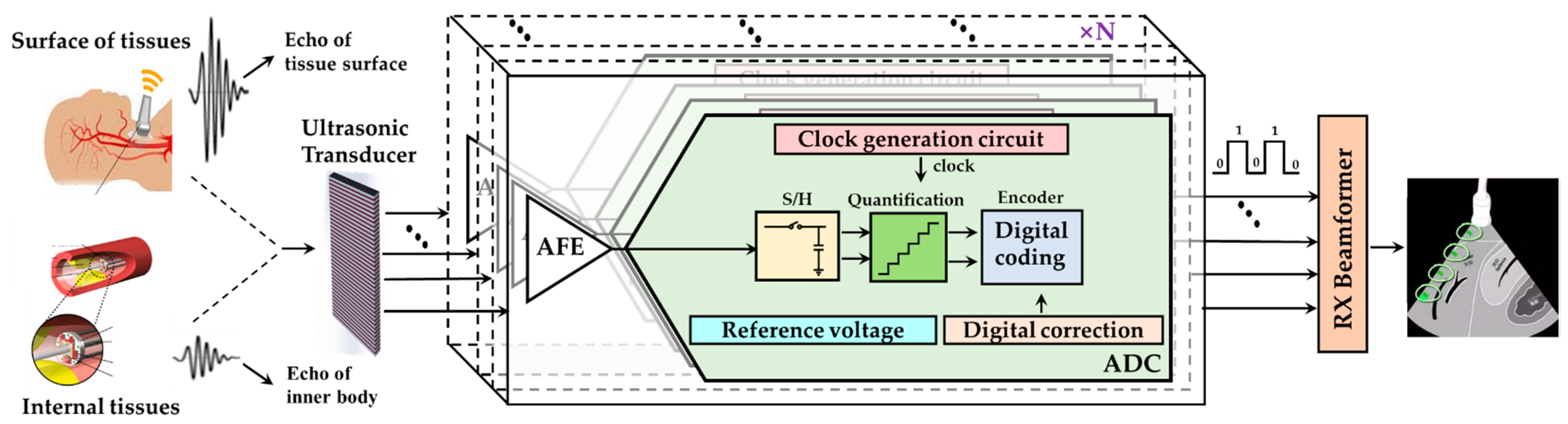
:1. Introduction
- (1)
- ADC is the main power consumption module in the UIS receiving chain. Power consumption exponentially increases with the channel number, and low power consumption becomes one of the main optimization directions of ADC.
- (2)
- In remote districts, only miniaturized or portable medical equipment is available due to uneven medical development. High integration and small size of receiver link (including ADC) chips are urgently needed for advanced portable or handy UIS devices.
- (3)
- Advanced UIS typically require high resolution and high-speed A/D data converters to improve ultrasonic imaging quality. Tradeoffs among sampling rate, signal to noise ratio (SNR), occupied area, and power consumption must be carefully considered.
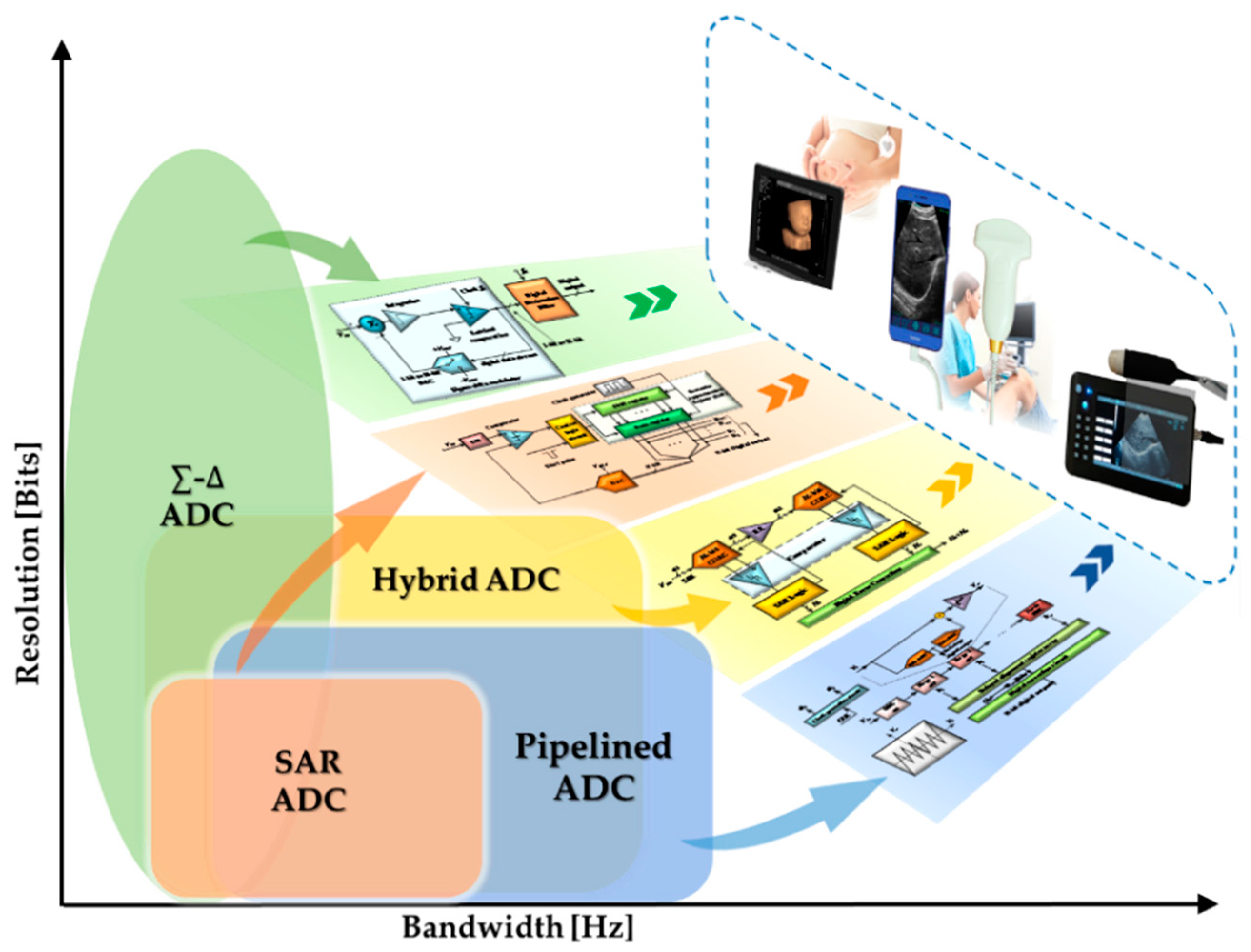
2. ADC for Miniaturized High-Resolution UIS
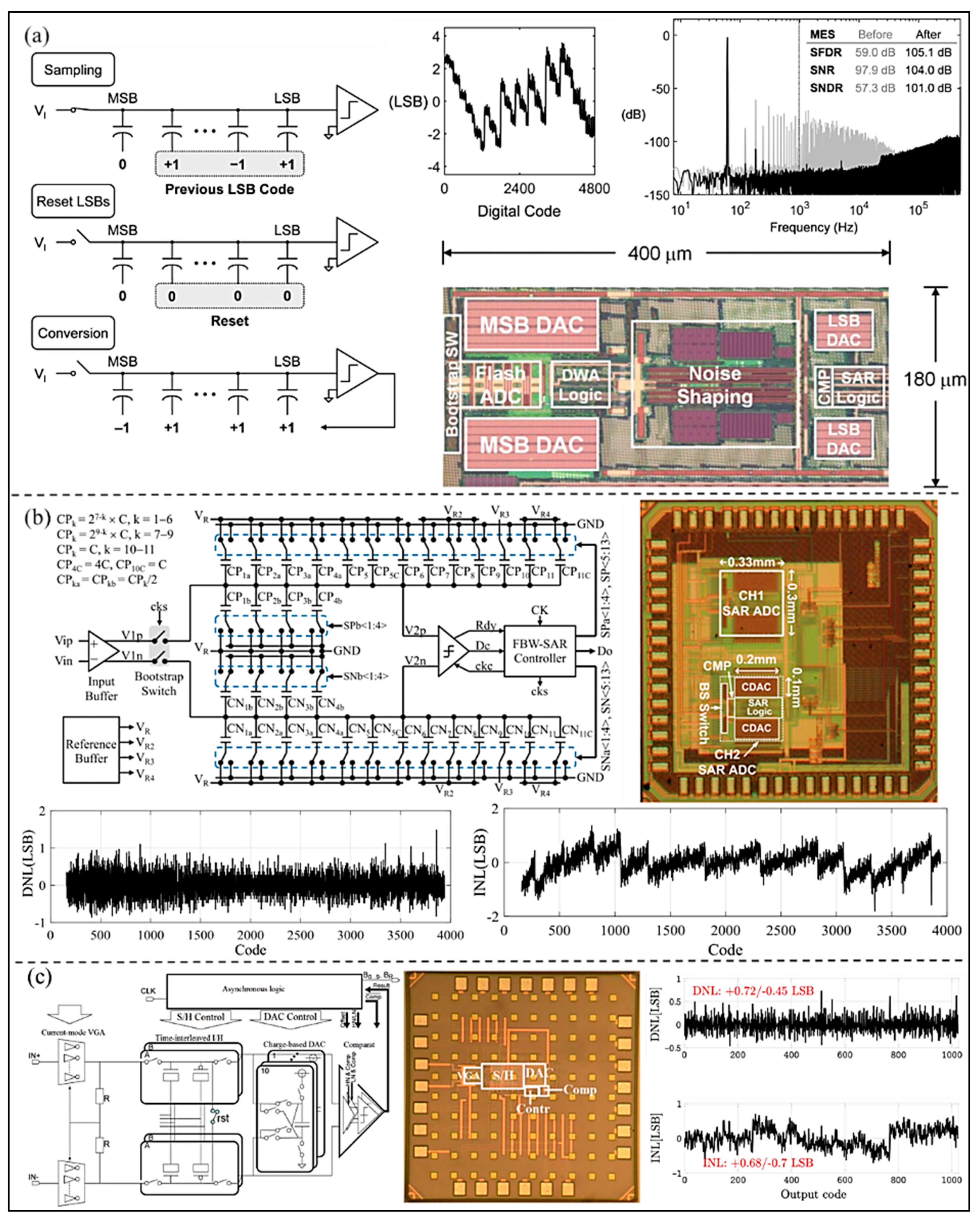
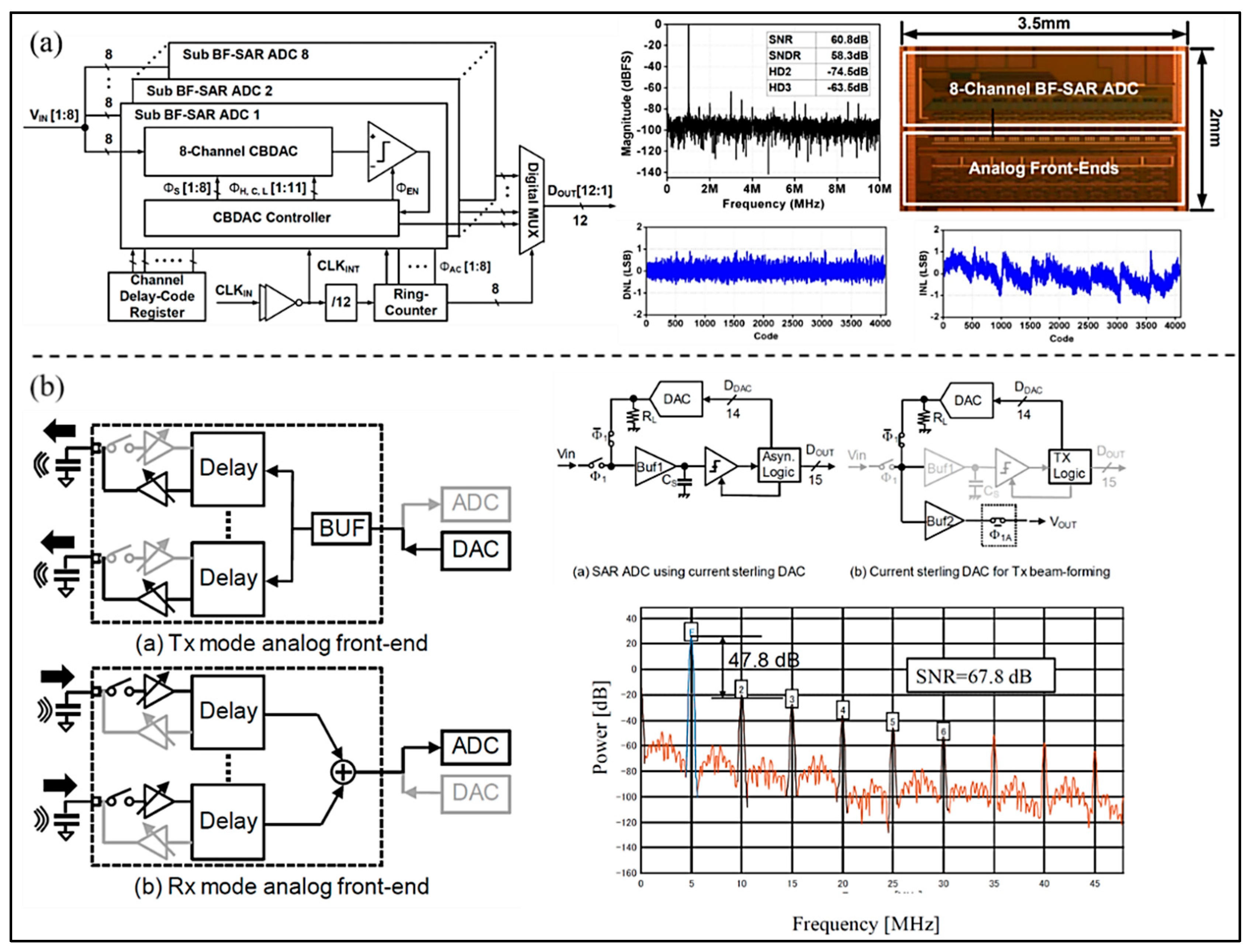
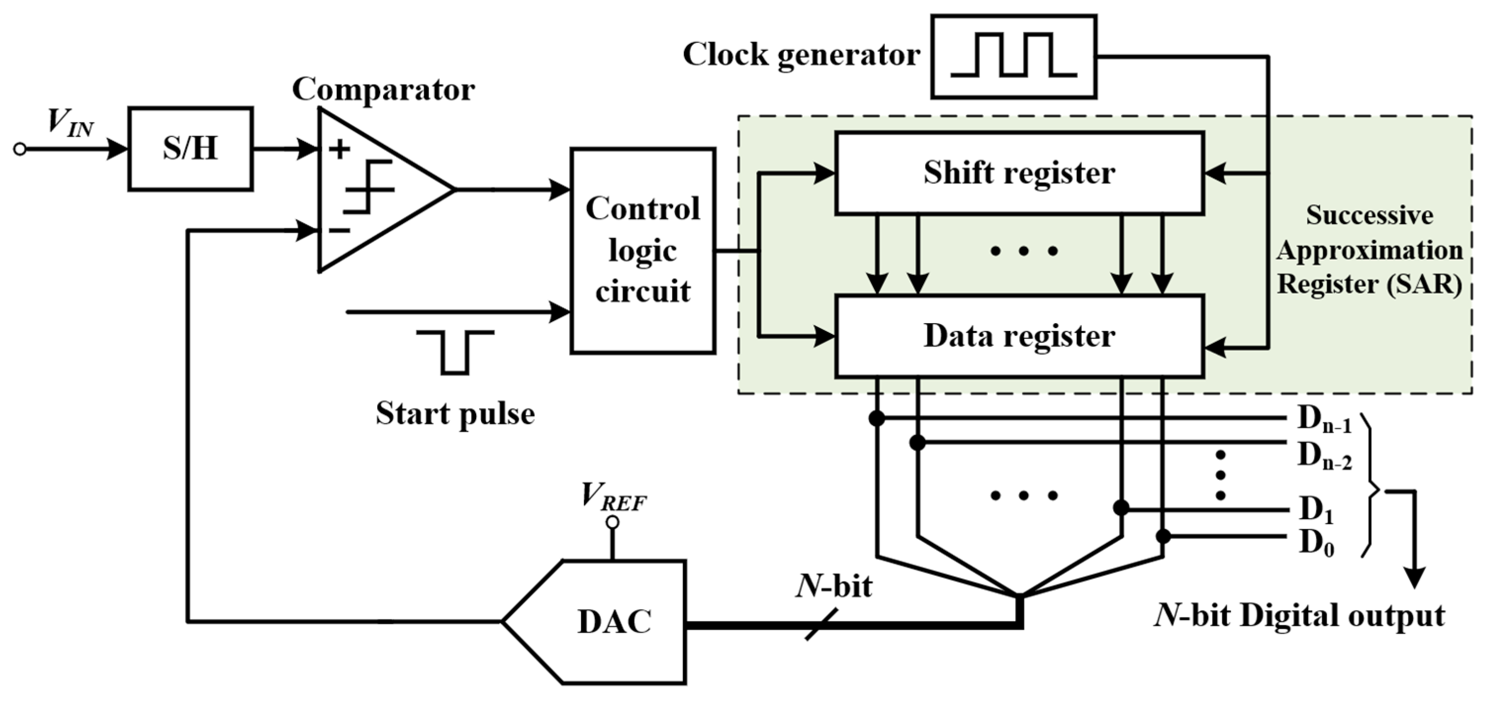
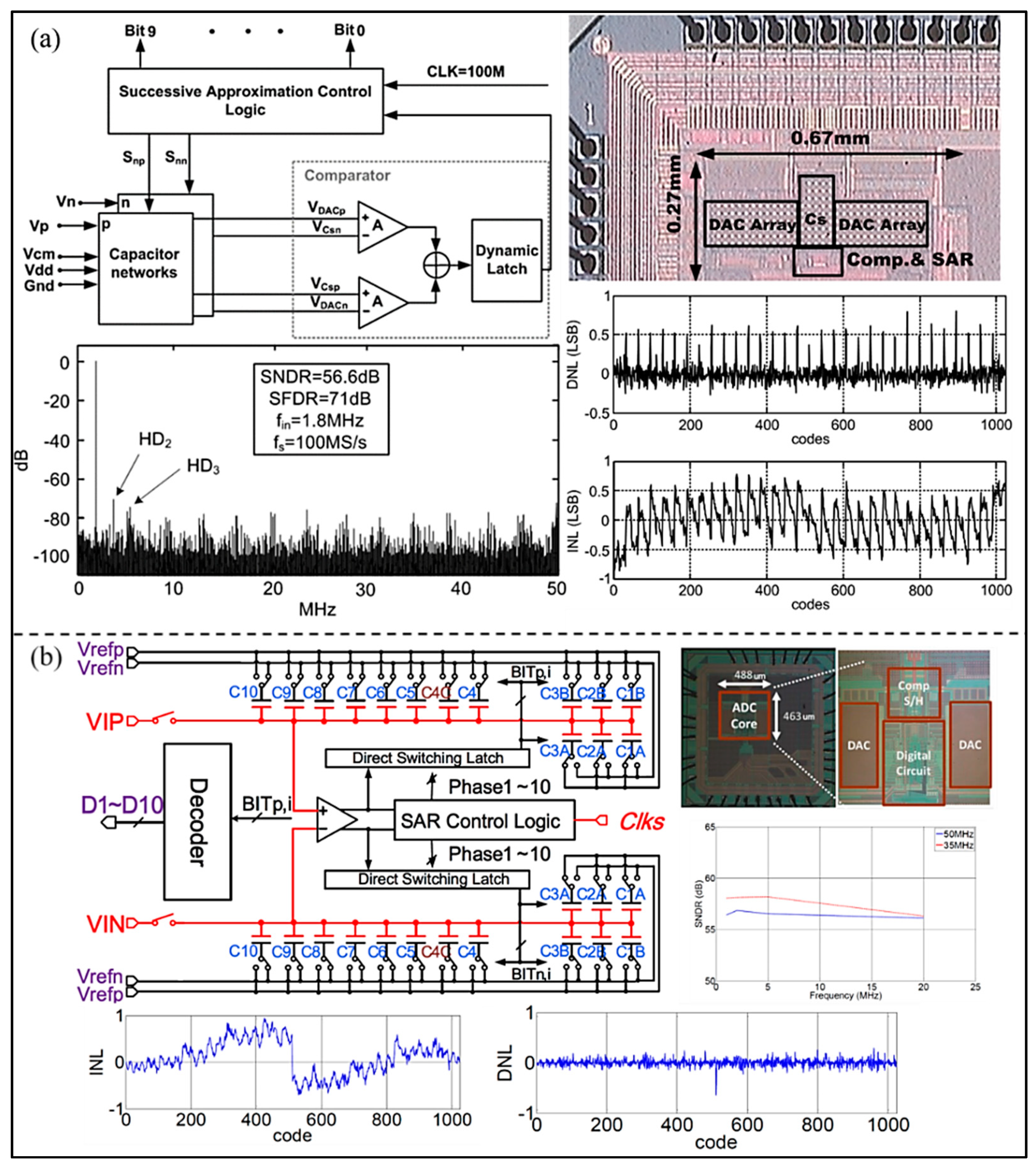
2.1. SAR ADC
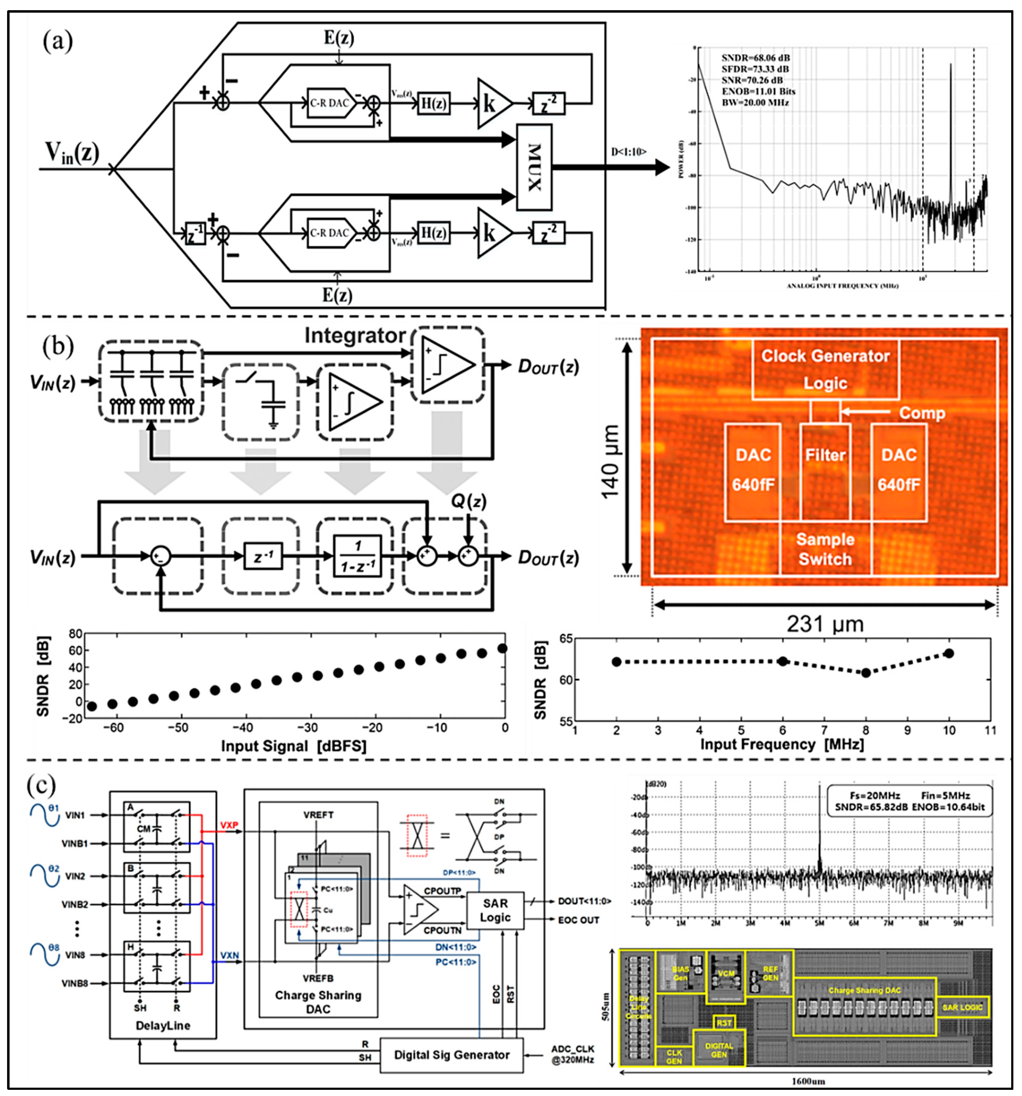
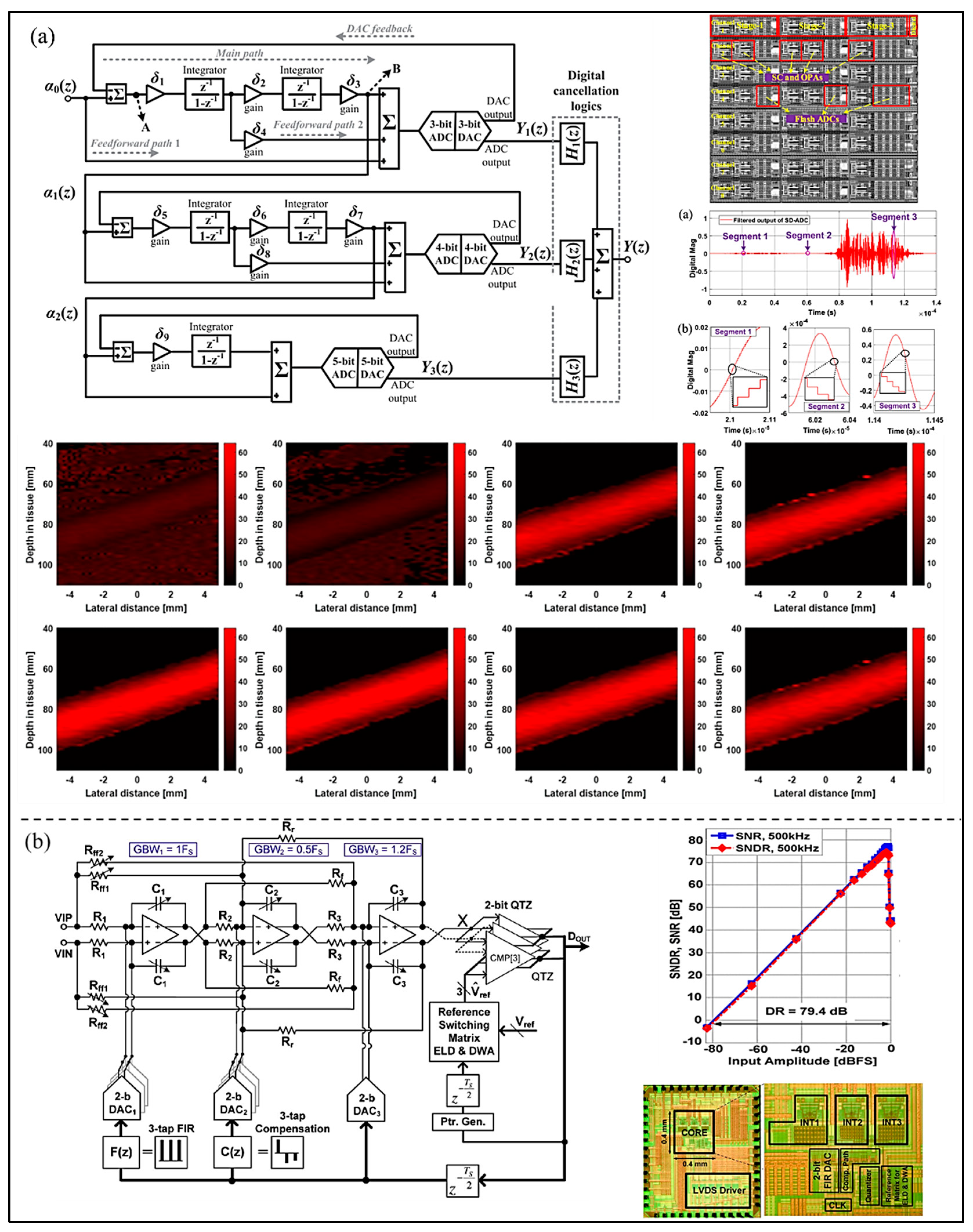
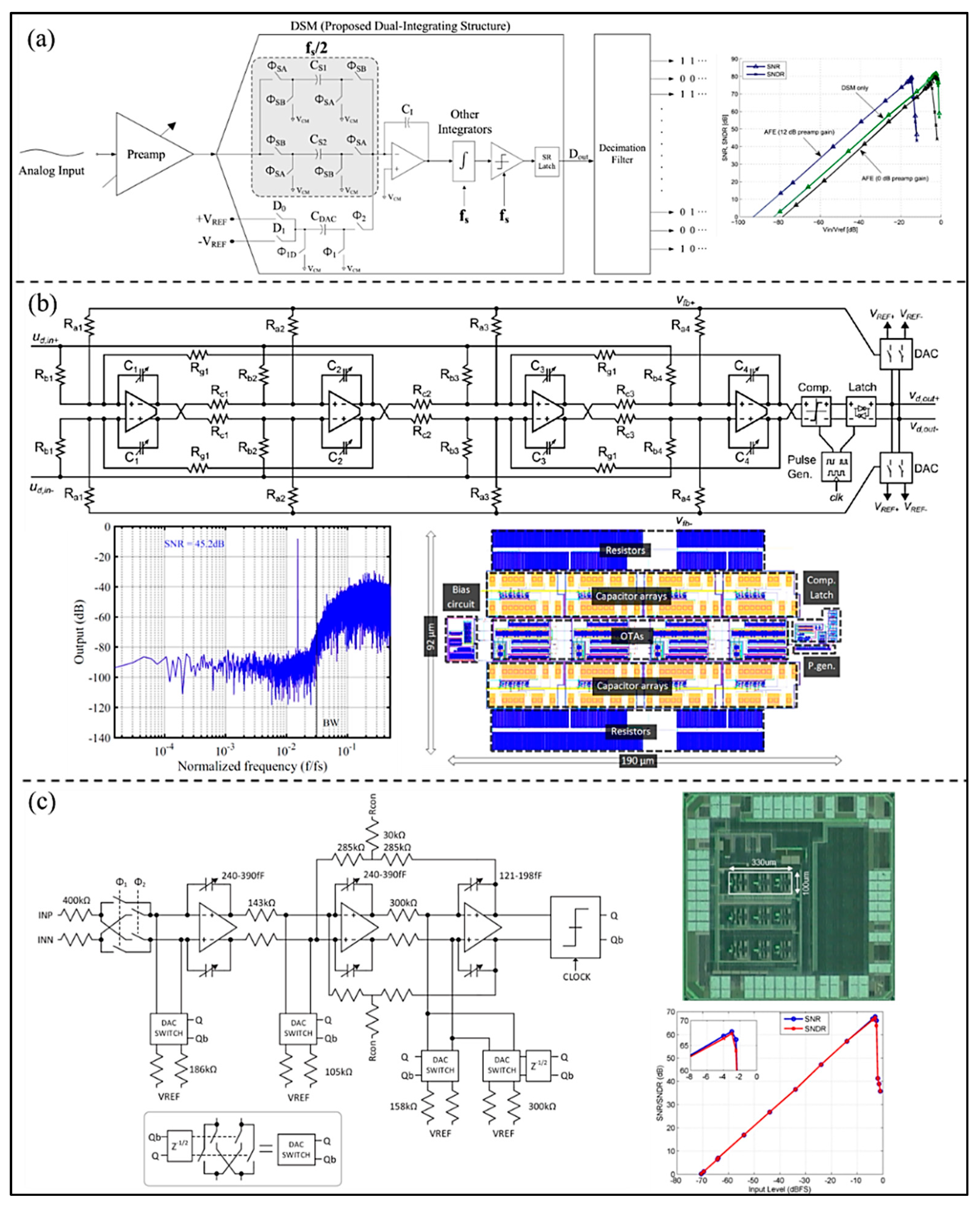
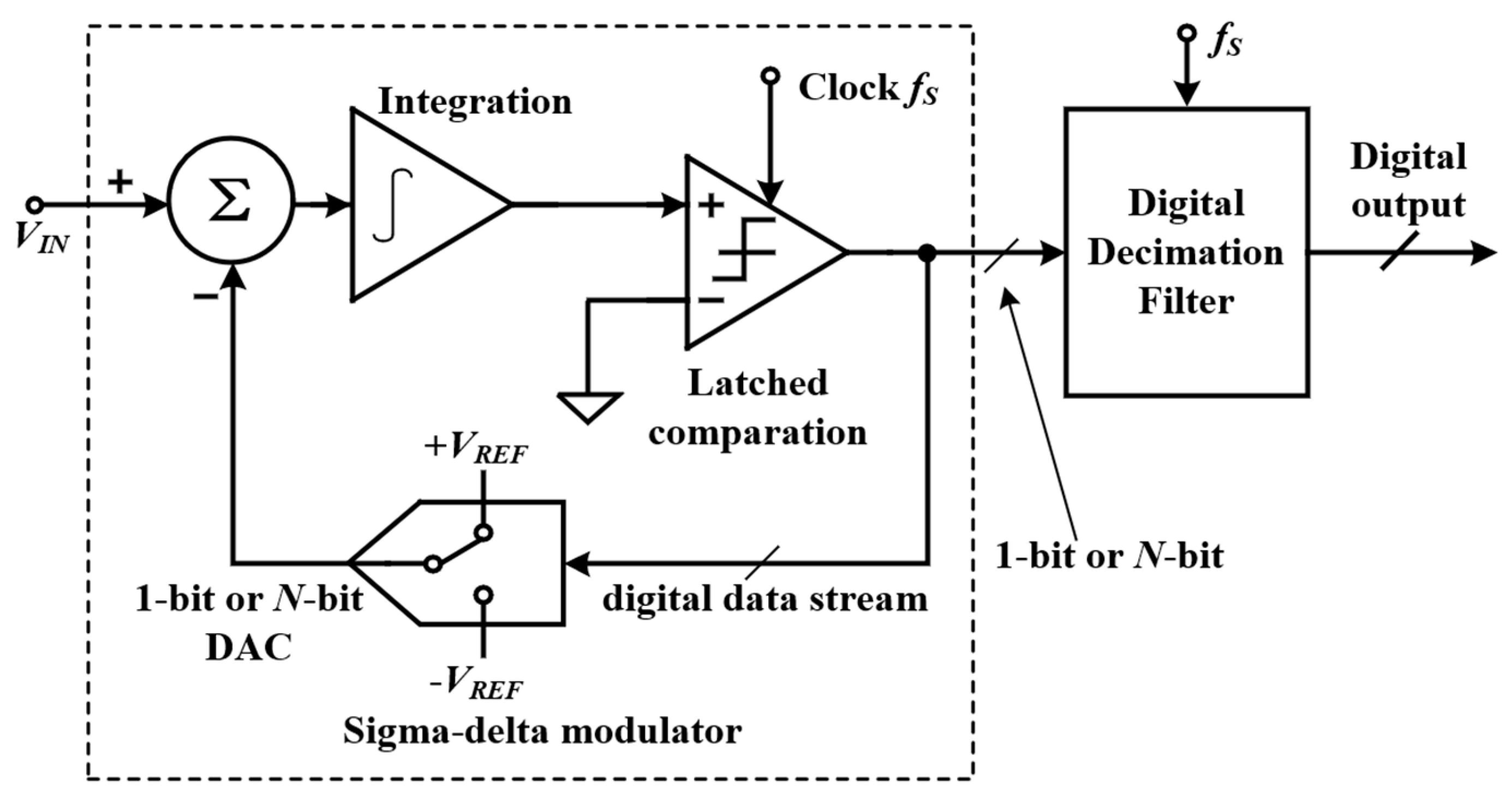
2.2. Sigma- Delta ADC
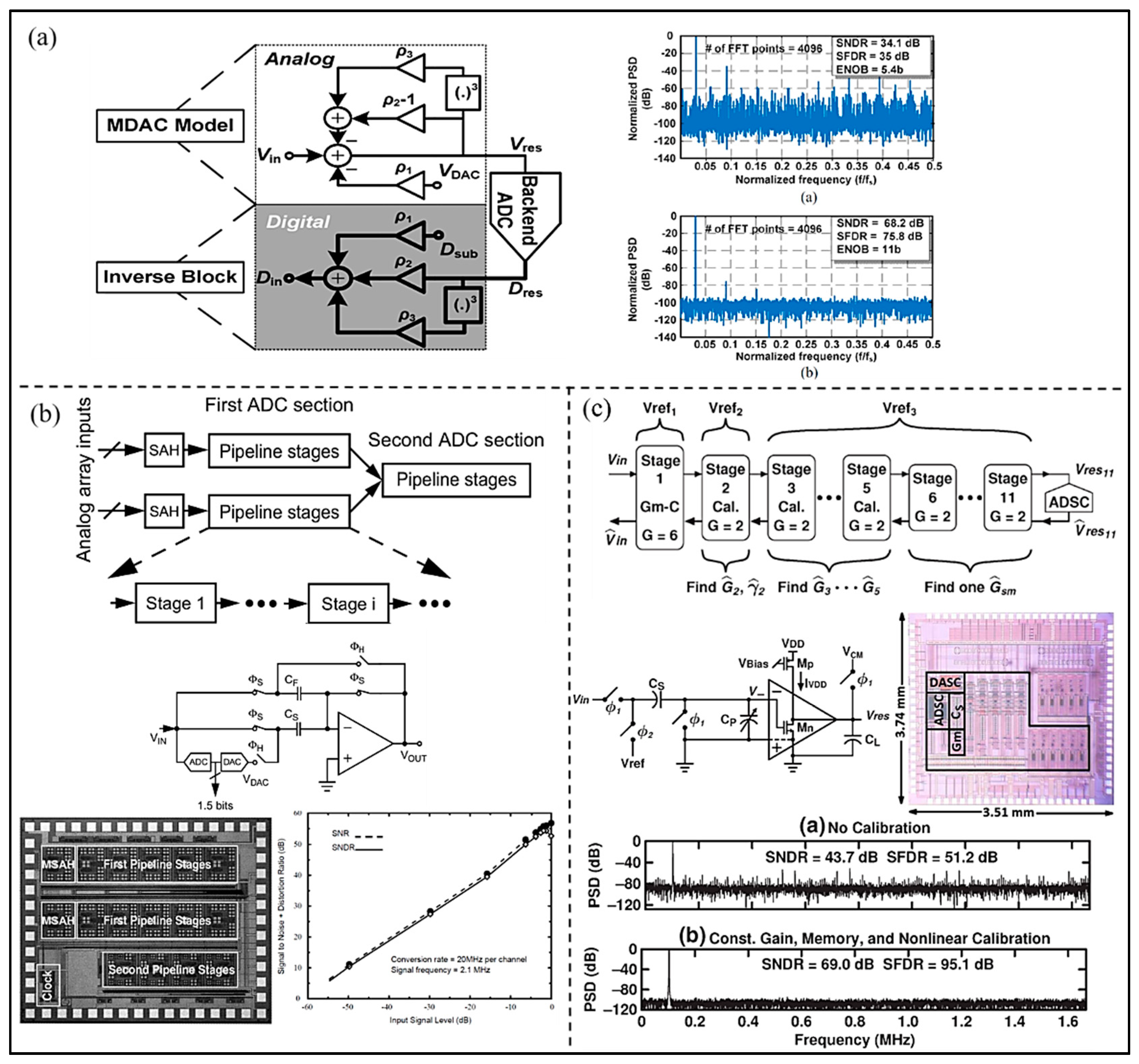
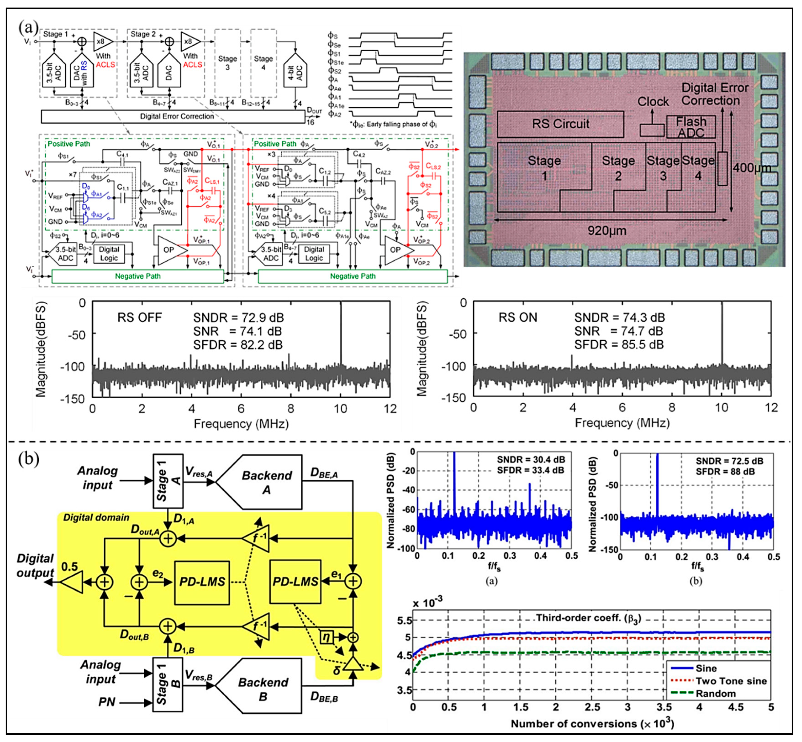
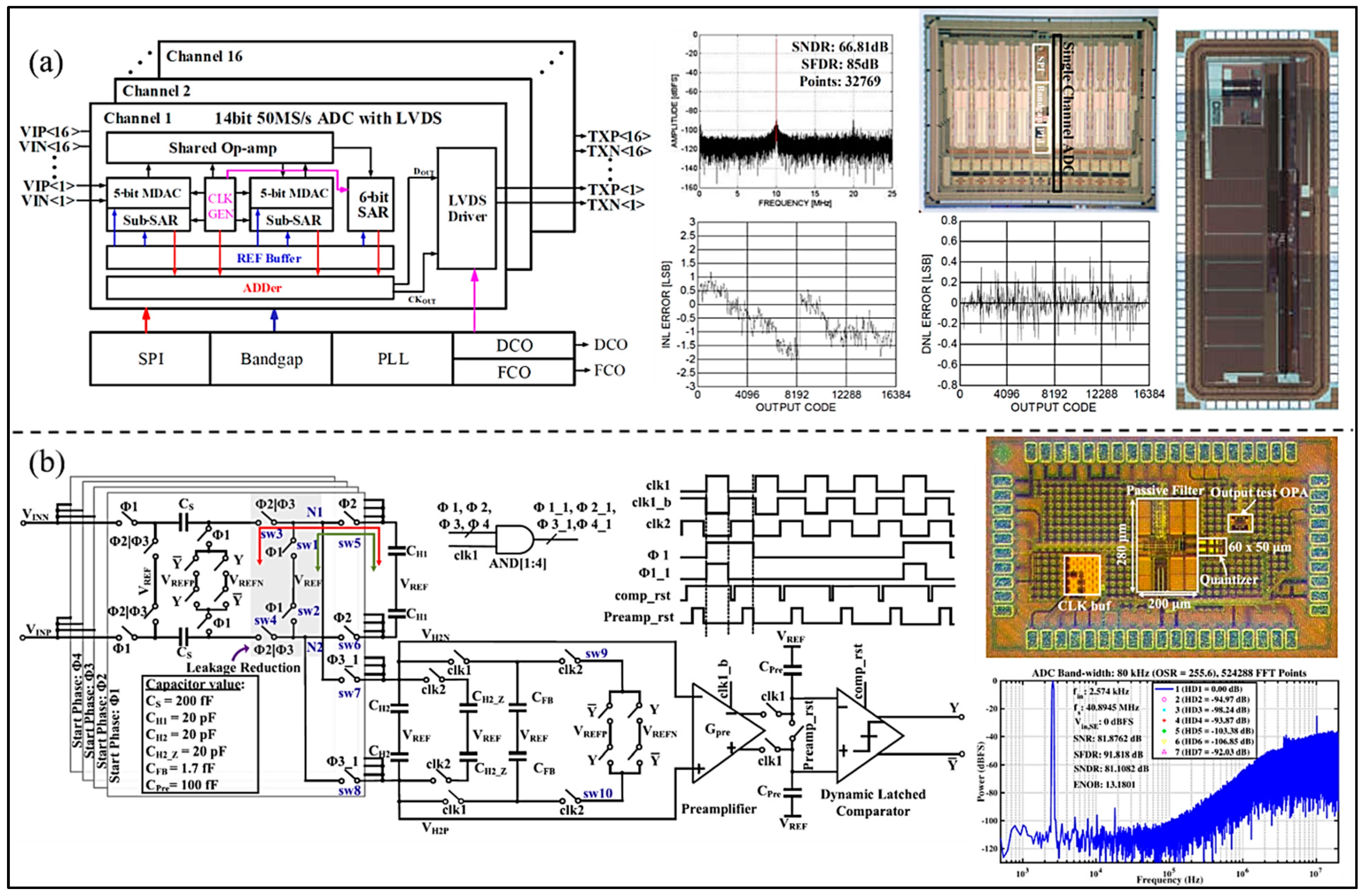
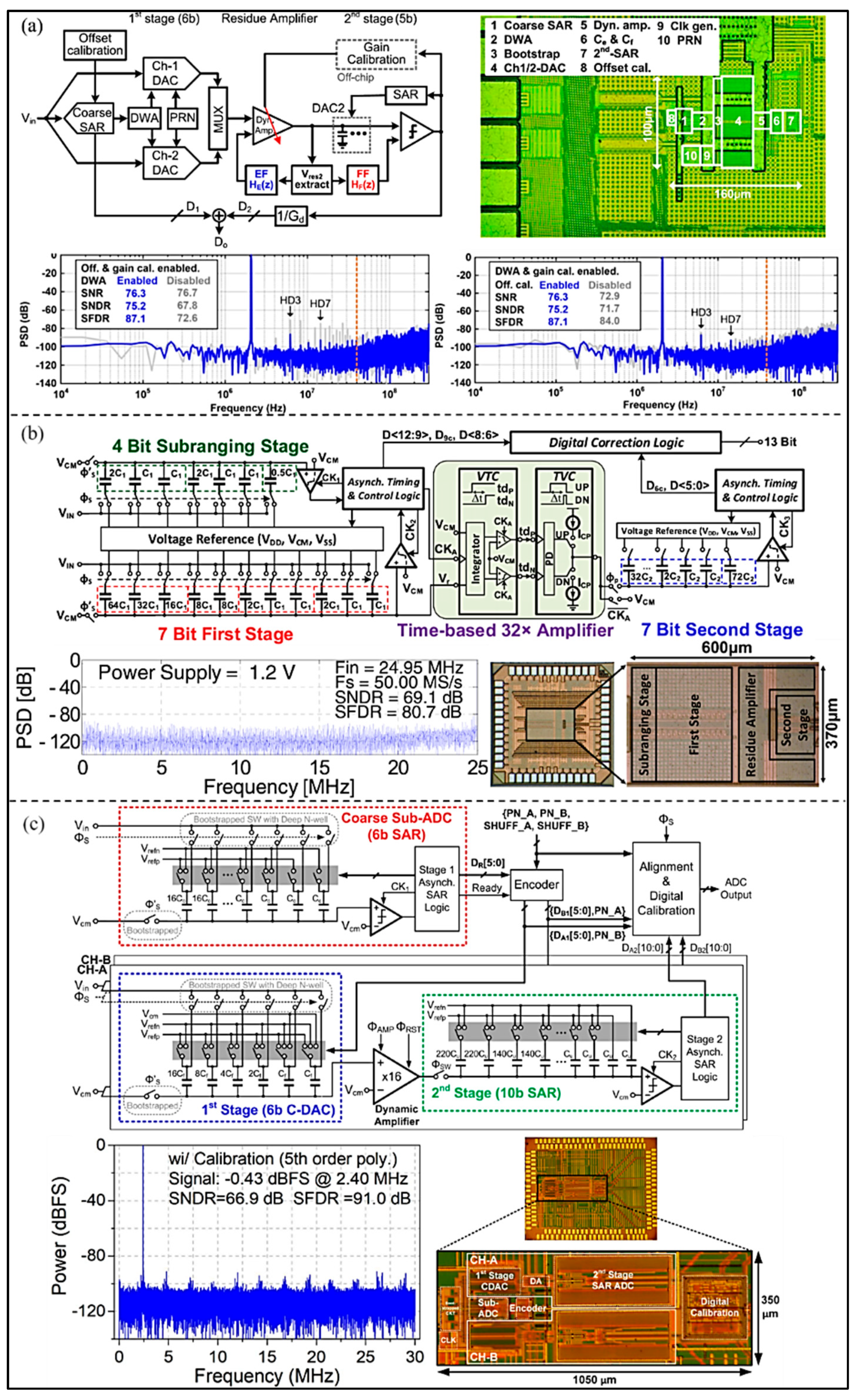
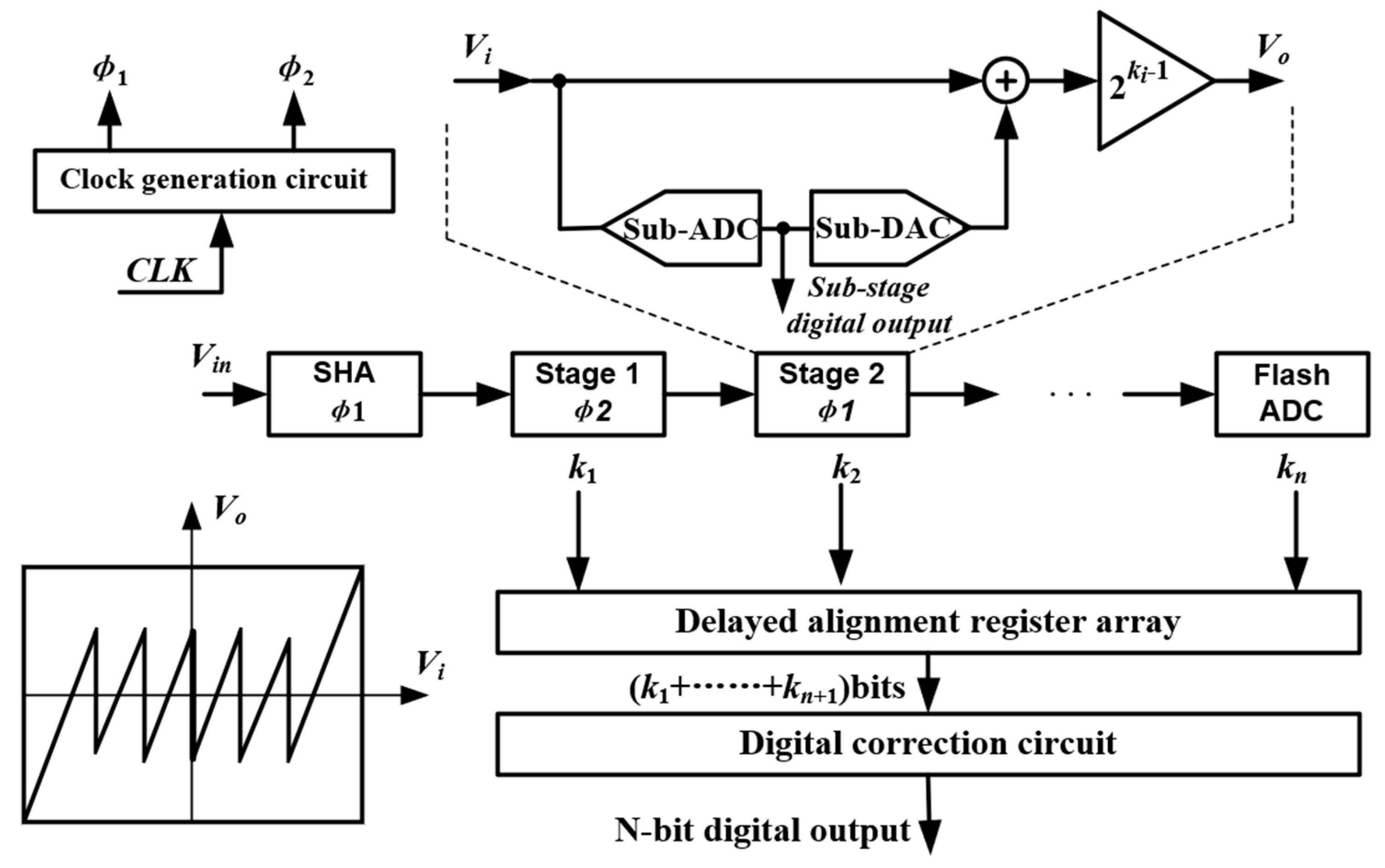
2.3. Pipelined ADC
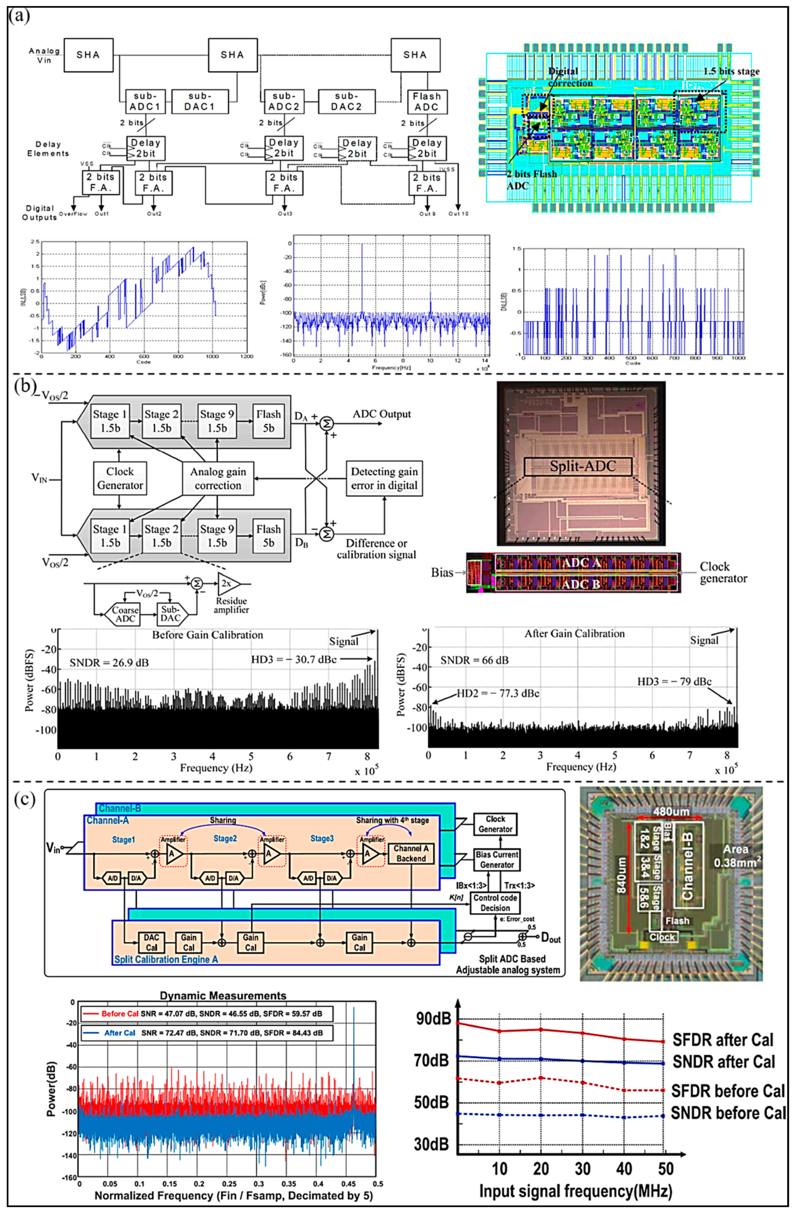
2.4. Hybrid ADC
3. Comparison and Discussion
4. Conclusions and Outlook
- 1.
- The integration of ADC ICs should be improved.
- Due to the compact size of capacitive micromachined ultrasonic transducer (CMUT) or piezoelectric micromachined ultrasonic transducer (PMUT) elements and the limited space available in the probe, efficient-area ICs design of the ADC, especially for multi-channel requirements, should be developed. Advanced fabrication process with smaller feature size is a fundamental way to improve the integration.
- It is worth considering that the ADC ICs can be bonding integrated with CMUT chips at the wafer level through silicon via (TSV) technology, but the packaging problem should be solved.
- The analog receiver front end, ADC, and microcontroller unit should be integrated in one chip as a system on chip (SoC) to improve the modules integration in the echo signal processing link of the UIS. In this way, miniaturization and low cost can be achieved, and high quality and low noise signal transmission ensured.
- Reducing the use of components is an important way to improve the IC integration. Shared circuit modules and small size capacitors (e.g., MIM capacitors) may be used in the detail circuit design. Novel compact and high-performance circuit structures should be further developed. Digital calibrations for error optimization and linearity improvement should be used as far as possible, rather than analog.
- 2.
- Ultra-low-power ultrasonic ADCs should be developed.
- Adopting of advanced fabrication processes means that ultra-low supply voltage can be used, which therefore reduces the power consumption of the ICs for UIS. This is also in good agreement with improving the integration of ultrasonic ICs. However, ultra-low voltage IC design technologies, such as current foldback, quasi-floating gate, etc., should be utilized.
- Nanowatt-level power consumption UIS ADCs are expected in the future. Ultra-low power IC design techniques, including bulk-driven, sub-threshold conduction, and current-reuse techniques, etc., can be adopted in the circuit design.
- Using as few devices or circuit modules as possible is another way to reduce the chip power consumption. Novel low-power circuit structures adopting circuit multiplexing scheme, inductor-less circuit structure, etc., should be further developed.
- 3.
- High resolution/speed ADCs should be investigated.
- High resolution ADC can be used for the developed UIS, such as the color Doppler imaging. Novel Σ-∆ ADC with resolution of higher than 24-bits and tens of MHz bandwidth should be further developed.
- Large bandwidth (high speed) ADC would be utilized to meet the requirement of high frequency UIS. Pipelined structure can be adopted, however, at the cost of more power consumption and chip area. A time interleaving scheme can be considered to greatly improve the data conversion rate.
- Hybrid ADC that can meet the requirements of both resolution and speed at the same time should be further developed.
- Digital correction technology needs to be developed to suppress or shape the mismatch noise generated by PVT variations, and therefore improve the linearity performance of the overall ADC. The dynamic element matching (DEM) technology is a very good choice and should be widely used in the circuit design.
Author Contributions
Funding
Conflicts of Interest
References
- Nikolaev, A.V.; de Jong, L.; Weijers, G.; Groenhuis, V.; Mann, R.M.; Siepel, F.J.; Maris, B.M.; Stramigioli, S.; Hansen, H.H.G.; de Korte, C.L. Quantitative Evaluation of an Automated Cone-Based Breast Ultrasound Scanner for MRI–3D US Image Fusion. IEEE Trans. Med. Imaging 2021, 40, 1229–1239. [Google Scholar] [CrossRef] [PubMed]
- McCarthy, C.; Camci-Unal, G. Low Intensity Pulsed Ultrasound for Bone Tissue Engineering. Micromachines 2021, 12, 1488. [Google Scholar] [CrossRef] [PubMed]
- Zhang, M.; Li, B.; Liu, Y.; Tang, R.; Lang, Y.; Huang, Q.; He, J. Different Modes of Low-Frequency Focused Ultrasound-Mediated Attenuation of Epilepsy Based on the Topological Theory. Micromachines 2021, 12, 1001. [Google Scholar] [CrossRef]
- Pei, Y.; Zhang, G.; Zhang, Y.; Zhang, W. Breast Acoustic Parameter Reconstruction Method Based on Capacitive Microm-achined Ultrasonic Transducer Array. Micromachines 2021, 12, 963. [Google Scholar] [CrossRef] [PubMed]
- Wang, S.; Housden, J.; Zar, A.; Gandecha, R.; Singh, D.; Rhode, K. Strategy for Monitoring Cardiac Interventions with an Intelligent Robotic Ultrasound Device †. Micromachines 2018, 9, 65. [Google Scholar] [CrossRef] [Green Version]
- Du, C.; Shih, B.; Wu, J.; Chiou, Y. Development of an AVF Stenosis Assessment Tool for Hemodialysis Patients Using Robotic Ultrasound System. Micromachines 2018, 9, 51. [Google Scholar] [CrossRef] [PubMed] [Green Version]
- Zhang, T.; Chen, R.; Zhang, Z.; Li, R.; Tang, X.; Wang, X.; Shung, K.K.; Zhou, Q. High frequency single crystal ultrasonic transducers up to 100 MHz for high resolution ophthalmic imaging applications. In Proceedings of the 2017 IEEE International Ultrasonics Symposium (IUS), Washington, DC, USA, 6–9 September 2017; pp. 1–4. [Google Scholar]
- Song, H.; Popovics, J.S.; Park, J. Development of an automated contactless ultrasonic scanning measurement system for wavefield imaging of concrete elements. In Proceedings of the 2017 IEEE International Ultrasonics Symposium (IUS), Washington, DC, USA, 6–9 September 2017; pp. 1–3. [Google Scholar] [CrossRef]
- Ma, T.; Yu, M.; Chen, Z.; Fei, C.; Shung, K.K.; Zhou, Q. Multi-frequency intravascular ultrasound (IVUS) imaging. IEEE Trans. Ultrason. Ferroelectr. Freq. Control 2015, 62, 97–107. [Google Scholar] [CrossRef] [PubMed] [Green Version]
- Herbert, E.; Pernot, M.; Larrat, B.; Montaldo, G.; Tanter, M.; Fink, M. Energy-based adaptive focusing of waves: Application to ultrasonic imaging and therapy. In Proceedings of the 2008 IEEE International Ultrasonics Symposium (IUS), Beijing, China, 2–5 November 2008; pp. 875–878. [Google Scholar] [CrossRef]
- Iula, A.; Savoia, A.; Longo, C.; Caliano, G.; Caronti, A.; Pappalardo, M. 3D Ultrasonic imaging of the human hand for biometric purposes. In Proceedings of the 2010 IEEE International Ultrasonics Symposium (IUS), San Diego, CA, USA, 11–14 October 2010; pp. 37–40. [Google Scholar]
- Vignon, F.; Aubry, J.; Tanter, M.; Fink, M. High resolution ultrasonic brain imaging: Noninvasive adaptive focusing based on twin arrays. In Proceedings of the 2004 IEEE Ultrasonics Symposium, Montreal, QC, Canada, 23–27 August 2004; pp. 231–234. [Google Scholar] [CrossRef]
- Alshaya, A.; Nie, L.; Cowell, D.M.J.; Carpenter, T.; McLaughlan, J.R.; Freear, S. Monitoring Needle Biopsy of Sentinel Lymph Nodes Using Photoacoustic Image with Dynamic-FDMAS Beamformer. In Proceedings of the 2019 IEEE International Ultrasonics Symposium (IUS), Glasgow, UK, 6–9 October 2019; pp. 490–493. [Google Scholar] [CrossRef]
- Kim, K.C.; Kim, M.J.; Joo, H.S.; Lee, W.; Yoon, C.; Song, T.K.; Yoo, Y. Smartphone-based portable ultrasound imaging system: A primary result. In Proceedings of the 2013 IEEE Interna-tional Ultrasonics Symposium (IUS), Prague, Czech Republic, 21–25 July 2013; pp. 2061–2063. [Google Scholar]
- Liu, S.; Tang, K.; Jin, H.; Zhang, R.; Kim, T.T.-H.; Zheng, Y. Continuous wave laser excitation based portable optoacoustic imaging system for melanoma detection. In Proceedings of the 2019 IEEE Biomedical Circuits and Systems Conference (BioCAS), Nara, Japan, 17–19 October 2019; pp. 1–4. [Google Scholar] [CrossRef]
- Kim, G.-D.; Yoon, C.; Kye, S.-B.; Lee, Y.; Kang, J.; Yoo, Y.; Song, T.-K. A single FPGA-based portable ultrasound imaging system for point-of-care applications. IEEE Trans. Ultrason. Ferroelectr. Freq. Control 2012, 59, 1386–1394. [Google Scholar] [CrossRef] [PubMed]
- Ahn, S.; Kang, J.; Kim, P.; Lee, G.; Jeong, E.; Jung, W.; Park, M.; Song, T.-K. Smartphone-based portable ultrasound imaging system: Prototype implementation and evaluation. In Proceedings of the 2015 IEEE International Ultrasonics Symposium (IUS), Taipei, Taiwan, 21–24 October 2015; pp. 1–4. [Google Scholar] [CrossRef]
- Chen, H.; Zheng, R.; Lou, E.; Le, L. Compact and Wireless Freehand 3D Ultrasound Real-time Spine Imaging System: A pilot study. In Proceedings of the 42nd Annual International Conference of the IEEE Engineering in Medicine & Biology Society (EMBC), Montreal, QC, Canada, 20–24 July 2020; pp. 2105–2108. [Google Scholar]
- Fuller, M.; Ranganathan, K.; Zhou, S.; Blalock, T.; Hossack, J.; Walker, W. Experimental System Prototype of a Portable, Low-Cost, C-Scan Ultrasound Imaging Device. IEEE Trans. Biomed. Eng. 2008, 55, 519–530. [Google Scholar] [CrossRef]
- Wygant, I.O.; Jamal, N.; Lee, H.J.; Nikoozadeh, A.; Zhuang, X.; Oralkan, O.; Ergun, A.S.; Karaman, M.; Khuri-Yakub, B.T. 2C-3 An Integrated Circuit with Transmit Beamforming and Parallel Receive Channels for 3D Ultrasound Imaging: Testing and Characterization. In Proceedings of the 2007 IEEE Ultrasonics Symposium Proceedings, New York, NY, USA, 28–31 October 2007; pp. 25–28. [Google Scholar] [CrossRef]
- Khuri-Yakub, B.T.; Karaman, M.; Oralkan, O.; Nikoozadeh, A.; Wygant, I.O.; Lee, H.; Yeh, D.T. P3H-6 An Integrated Circuit with Transmit Beamforming and Parallel Receive Channels for Real-Time Three-Dimensional Ultrasound Imaging. In Proceedings of the 2006 IEEE Ultrasonics Symposiums, Vancouver, BC, Canada, 2–6 October 2006; pp. 2186–2189. [Google Scholar] [CrossRef]
- Bhuyan, A.; Choe, J.W.; Lee, B.C.; Wygant, I.O.; Nikoozadeh, A.; Oralkan, O.; Khuri-Yakub, B.T. Integrated Circuits for Volumetric Ultrasound Imaging With 2-D CMUT Arrays. IEEE Trans. Biomed. Circuits Syst. 2014, 7, 796–804. [Google Scholar] [CrossRef]
- Winckler, C.A.; Smith, P.R.; Cowell, D.M.J.; Olagunju, O.E.; Freear, S. The design of a high speed receiver system for an ultrasound array research platform. In Proceedings of the 2012 IEEE International Ultrasonics Symposium, Dresden, Germany, 7–10 October 2012; pp. 1481–1484. [Google Scholar] [CrossRef]
- Di Ianni, T.; Hemmsen, M.C.; Muntal, P.L.; Jorgensen, I.H.H.; Jensen, J.A. System-Level Design of an Integrated Receiver Front End for a Wireless Ultrasound Probe. IEEE Trans. Ultrason. Ferroelectr. Freq. Control 2016, 63, 1935–1946. [Google Scholar] [CrossRef] [Green Version]
- Berkol, G.; Baltus, P.G.M.; Harpe, P.J.A.; Cantatore, E. A 1.25 μJ per Measurement Ultrasound Rangefinder System in 65 nm CMOS for Explorations with a Swarm of Sensor Nodes. IEEE Trans. Circuits Syst. I Regul. Pap. 2021, 68, 1409–1420. [Google Scholar] [CrossRef]
- Chen, D.; Wang, L.; Luo, X.; Fei, C.; Li, D.; Shan, G.; Yang, Y. Recent Development and Perspectives of Optimization Design Methods for Piezoelectric Ultrasonic Transducers. Micromachines 2021, 12, 779. [Google Scholar] [CrossRef]
- Chen, D.; Zhao, J.; Fei, C.; Li, D.; Zhu, Y.; Li, Z.; Guo, R.; Lou, L.; Feng, W.; Yang, Y. Particle Swarm Optimization Algorithm-Based Design Method for Ultrasonic Transducers. Micromachines 2020, 11, 715. [Google Scholar] [CrossRef] [PubMed]
- Li, D.; Fei, C.; Zhang, Q.; Li, Y.; Yang, Y. A 20-MHz BW MASH Sigma–Delta Modulator with Mismatch Noise Randomization for Multi-Bit DACs. J. Circuits Syst. Comput. 2019, 29, 2050108. [Google Scholar] [CrossRef]
- Li, D.; Fei, C.; Zhang, Q.; Li, Y.; Yang, Y.; Zhou, Q. Ultrahigh Frequency Ultrasonic Transducers Design with Low Noise Amplifier Integrated Circuit. Micromachines 2018, 9, 515. [Google Scholar] [CrossRef] [PubMed] [Green Version]
- Wu, X.; Sanders, J.; Zhang, X.; Yamaner, F.; Oralkan, Ö. A high-frequency and high-frame-rate ultrasound imaging system design for capacitive micromachined ultrasonic transducer arrays on an FPGA evaluation board. In Proceedings of the 2017 IEEE International Ultrasonics Symposium (IUS), Washington, DC, USA, 6–9 September 2017; p. 1. [Google Scholar] [CrossRef]
- Tan, M.; Chen, C.; Chen, Z.; Janjic, J.; Daeichin, V.; Chang, Z.-Y.; Noothout, E.; van Soest, G.; Verweij, M.D.; de Jong, N.; et al. A Front-End ASIC With High-Voltage Transmit Switching and Receive Digitization for 3-D Forward-Looking Intravascular Ultrasound Imaging. IEEE J. Solid-State Circuits 2018, 53, 2284–2297. [Google Scholar] [CrossRef] [Green Version]
- Gurun, G.; Tekes, C.; Zahorian, J.; Xu, T.; Satir, S.; Karaman, M.; Hasler, J.; Degertekin, F.L. Single-chip CMUT-on-CMOS front-end system for real-time volumetric IVUS and ICE imaging. IEEE Trans. Ultrason. Ferroelectr. Freq. Control 2014, 61, 239–250. [Google Scholar] [CrossRef] [PubMed] [Green Version]
- Yu, Z.; Blaak, S.; Chang, Z.-Y.; Yao, J.; Bosch, J.G.; Prins, C.; Lancée, C.T.; De Jong, N.; Pertijs, M.A.P.; Meijer, G.C.M. Front-end receiver electronics for a matrix transducer for 3-D transesophageal echocardiography. IEEE Trans. Ultrason. Ferroelectr. Freq. Control 2012, 59, 1500–1512. [Google Scholar] [CrossRef]
- Bozkurt, A.; Karaman, M. Design of a front-end integrated circuit for 3D acoustic imaging using 2D CMUT arrays. IEEE Trans. Ultrason. Ferroelectr. Freq. Control 2005, 52, 2235–2241. [Google Scholar] [CrossRef]
- Shu, Y.-S.; Kuo, L.-T.; Lo, T.-Y. An Oversampling SAR ADC With DAC Mismatch Error Shaping Achieving 105 dB SFDR and 101 dB SNDR Over 1 kHz BW in 55 nm CMOS. IEEE J. Solid-State Circuits 2016, 51, 2928–2940. [Google Scholar] [CrossRef]
- Chung, Y.-H.; Yen, C.-W.; Tsai, P.-K.; Chen, B.-W. A 12-bit 40-MS/s SAR ADC with a Fast-Binary-Window DAC Switching Scheme. IEEE Trans. Very Large Scale Integr. (VLSI) Syst. 2018, 26, 1989–1998. [Google Scholar] [CrossRef]
- Malki, B.; Yamamoto, T.; Verbruggen, B.; Wambacq, P.; Craninckx, J. A 70dB DR 10b 0-to-80MS/s current-integrating SAR ADC with adaptive dynamic range. In Proceedings of the 2012 IEEE International Solid-State Circuits Conference, San Francisco, CA, USA, 19–23 February 2012; pp. 470–472. [Google Scholar] [CrossRef]
- Li, S.; Diao, J.; Wu, Y.; Ye, F.; Ren, J. A 20MHz Bandwidth Band-Pass Noise-Shaping SAR ADC with OPAMP Sharing Switched-Capacitor Filter. In Proceedings of the 2019 IEEE 62nd International Midwest Symposium on Circuits and Systems (MWSCAS), Dallas, TX, USA, 4–7 August 2019; pp. 109–112. [Google Scholar]
- Fredenburg, J.A.; Flynn, M.P. A 90-MS/s 11-MHz-Bandwidth 62-dB SNDR Noise-Shaping SAR ADC. IEEE J. Solid-State Circuits 2012, 47, 2898–2904. [Google Scholar] [CrossRef]
- Lee, J.; Lee, K. A Design of 20MS/s 12-bit Charge Sharing SAR ADC for Ultrasound Diagnostic Medical. In Proceedings of the 2021 Twelfth International Conference on Ubiquitous and Future Networks (ICUFN), Jeju Island, Korea, 17–20 August 2021; pp. 239–241. [Google Scholar]
- Zhu, Y.; Chan, C.-H.; Chio, U.-F.; Sin, S.-W.; Seng-Pan, U.; Martins, R.P.; Maloberti, F. A 10-bit 100-MS/s Reference-Free SAR ADC in 90 nm CMOS. IEEE J. Solid-State Circuits 2010, 45, 1111–1121. [Google Scholar] [CrossRef]
- Xu, Y.; Ytterdal, T. A 7-bit 50ms/s single-ended asynchronous SAR ADC in 65nm CMOS. In Proceedings of the 2013 NORCHIP, Vilnius, Lithuania, 11–12 November 2013; pp. 1–4. [Google Scholar] [CrossRef]
- Tsai, W.; Kuo, C.; Chang, S.; Lo, L.; Wu, Y.; Chen, C. A 10-bit 50-MS/s SAR ADC for dual-voltage domain portable systems. In Proceedings of the 2015 IEEE International Symposium on Circuits and Systems (ISCAS), Lisbon, Portugal, 24–27 May 2015; pp. 2425–2428. [Google Scholar]
- Chen, C.; Chen, Z.; Bera, D.; Noothout, E.; Chang, Z.-Y.; Vos, H.; Bosch, J.; Verweij, M.; de Jong, N.; Pertijs, M. A front-end ASIC for miniature 3-D ultrasound probes with in-probe receive digitization. In Proceedings of the 2017 IEEE International Ultrasonics Symposium (IUS), Washington, DC, USA, 6–9 September 2017; pp. 1–4. [Google Scholar] [CrossRef]
- Kim, T.; Kim, S. A 12.1mW, 60dB SNR, 8-channel beamforming embedded SAR ADC for ultrasound imaging systems. In Proceedings of the 2017 IEEE Asian Solid-State Circuits Conference (A-SSCC), Seoul, Korea, 6–8 November 2017; pp. 141–144. [Google Scholar]
- Yazaki, T.; Hyogo, A. Time-Shared DAC in SAR ADC for Tx Beamforming of Ultrasound Application. In Proceedings of the 2018 International Symposium on Intelligent Signal Processing and Communication Systems (ISPACS), Ishigaki, Japan, 27–30 November 2018; pp. 453–456. [Google Scholar]
- Li, D.; Qian, X.; Li, R.; Fei, C.; Jiang, L.; Chen, X.; Yang, Y.; Zhou, Q. High Resolution ADC for Ultrasound Color Doppler Imaging Based on MASH Sigma-Delta Modulator. IEEE Trans. Biomed. Eng. 2020, 67, 1438–1449. [Google Scholar] [CrossRef]
- Zhang, Y.; Chen, C.; He, T.; Temes, G.C. A Continuous-Time Delta-Sigma Modulator for Biomedical Ultrasound Beamformer Using Digital ELD Compensation and FIR Feedback. IEEE Trans. Circuits Syst. I Regul. Pap. 2015, 62, 1689–1698. [Google Scholar] [CrossRef]
- Yoon, Y.; Duan, Q.; Yeo, J.; Roh, J.; Kim, J.; Kim, N. A Delta–Sigma Modulator for Low-Power Analog Front Ends in Biomedical Instrumentation. IEEE Trans. Instrum. Meas. 2016, 65, 1530–1539. [Google Scholar] [CrossRef]
- Muntal, P.L.; Jørgensen, I.H.H.; Bruun, E. A continuous-time delta-sigma ADC for portable ultrasound scanners. Analog. Integr. Circuits Signal Process. 2017, 92, 393–402. [Google Scholar] [CrossRef]
- Kaald, R.; Eggen, T.; Ytterdal, T. A 1 MHz BW 34.2 fJ/step Continuous Time Delta Sigma Modulator with an Integrated Mixer for Cardiac Ultrasound. IEEE Trans. Biomed. Circuits Syst. 2016, 11, 234–243. [Google Scholar] [CrossRef]
- Chirala, M.; Huynh, P.; Ryu, J.; Kim, Y. A 128-ch Δ–Σ ADC based mixed signal IC for full digital beamforming Wireless handheld Ultrasound imaging system. In Proceedings of the 2015 37th Annual International Conference of the IEEE Engineering in Medicine and Biology Society (EMBC), Milan, Italy, 25–29 August 2015; pp. 1339–1342. [Google Scholar]
- Chen, M.-C.; Perez, A.P.; Kothapalli, S.-R.; Cathelin, P.; Cathelin, A.; Gambhir, S.S.; Murmann, B. A Pixel Pitch-Matched Ultrasound Receiver for 3-D Photoacoustic Imaging with Integrated Delta-Sigma Beamformer in 28-nm UTBB FD-SOI. IEEE J. Solid-State Circuits 2017, 52, 2843–2856. [Google Scholar] [CrossRef]
- D’Urbino, M.; Chen, C.; Chen, Z.; Chang, Z.-Y.; Ponte, J.; Lippe, B.; Pertijs, M. An Element-Matched Electromechanical ΔΣ ADC for Ultrasound Imaging. IEEE J. Solid-State Circuits 2018, 53, 2795–2805. [Google Scholar] [CrossRef]
- Gholami, P.; Yavari, M. Digital Background Calibration with Histogram of Decision Points in Pipelined ADCs. IEEE Trans. Circuits Syst. II Express Briefs 2017, 65, 16–20. [Google Scholar] [CrossRef]
- Kaviani, K.; Oralkan, O.; Khuri-Yakub, P.; Wooley, B. A multichannel pipeline analog-to-digital converter for an integrated 3-D ultrasound imaging system. IEEE J. Solid-State Circuits 2003, 38, 1266–1270. [Google Scholar] [CrossRef]
- Wang, D.; Keane, J.P.; Hurst, P.J.; Lewis, S.H. An Integrator-Based Pipelined ADC with Digital Calibration. IEEE Trans. Circuits Syst. II Express Briefs 2015, 62, 831–835. [Google Scholar] [CrossRef]
- El-Sankary, K.; Kassem, A.; Chebli, R.; Sawan, M. Low power, low voltage, 10bit-50MSPS pipeline ADC dedicated for front-end ultrasonic receivers. In Proceedings of the 14th International Conference on Microelectronics, Beirut, Lebanon, 11–13 December 2002; pp. 219–222. [Google Scholar]
- Akter, S.; Sehgal, R.; van der Goes, F.; Makinwa, K.A.A.; Bult, K. A 66-dB SNDR Pipelined Split-ADC in 40-nm CMOS Using a Class-AB Residue Amplifier. IEEE J. Solid-State Circuits 2018, 53, 2939–2950. [Google Scholar] [CrossRef] [Green Version]
- Mao, J.; Guo, M.; Sin, S.-W.; Martins, R.P. A 14-Bit Split-Pipeline ADC with Self-Adjusted Opamp-Sharing Duty-Cycle and Bias Current. IEEE Trans. Circuits Syst. II Express Briefs 2018, 65, 1380–1384. [Google Scholar] [CrossRef]
- Hung, T.-C.; Kuo, T.-H. A 75.3-dB SNDR 24-MS/s Ring Amplifier-Based Pipelined ADC Using Averaging Correlated Level Shifting and Reference Swapping for Reducing Errors From Finite Opamp Gain and Capacitor Mismatch. IEEE J. Solid-State Circuits 2019, 54, 1425–1435. [Google Scholar] [CrossRef]
- Montazerolghaem, M.A.; Moosazadeh, T.; Yavari, M. A Predetermined LMS Digital Background Calibration Technique for Pipelined ADCs. IEEE Trans. Circuits Syst. II Express Briefs 2015, 62, 841–845. [Google Scholar] [CrossRef]
- Kwon, Y.; Kim, T.; Sun, N.; Chae, Y. A 348-μW 68.8-dB SNDR 20-MS/s Pipelined SAR ADC with a Closed-Loop Two-Stage Dynamic Amplifier. IEEE Solid-State Circuits Lett. 2021, 4, 166–169. [Google Scholar] [CrossRef]
- Zhang, H.; Sun, J.; Zhang, J.; Zhang, R.; Carusone, A.C. A Low-Power Pipelined-SAR ADC Using Boosted Bucket-Brigade Device for Residue Charge Processing. IEEE Trans. Very Large Scale Integr. (VLSI) Syst. 2018, 26, 1763–1776. [Google Scholar] [CrossRef]
- Wu, Y.; Lan, J.; Chen, M.; Ye, F.; Ren, J. A 16-channel 50MS/s 14bit Pipelined-SAR ADC for Integrated Ultrasound Imaging Systems. In Proceedings of the 2020 IEEE Asia Pacific Conference on Circuits and Systems (APCCAS), Ha Long, Vietnam, 8–10 December 2020; pp. 3–6. [Google Scholar] [CrossRef]
- Wang, H.; Schembari, F.; Staszewski, R. Passive SC ΔΣ Modulator Based on Pipelined Charge-Sharing Rotation in 28-nm CMOS. IEEE Trans. Circuits Syst. I Regul. Pap. 2020, 67, 578–589. [Google Scholar] [CrossRef]
- Song, Y.; Zhu, Y.; Chan, C.-H.; Martins, R.P. A 40-MHz Bandwidth 75-dB SNDR Partial-Interleaving SAR-Assisted Noise-Shaping Pipeline ADC. IEEE J. Solid-State Circuits 2020, 56, 1772–1783. [Google Scholar] [CrossRef]
- Zhang, M.; Noh, K.; Fan, X.; Sánchez-Sinencio, E.A. A 0.8–1.2 V 10–50 MS/s 13-bit Subranging Pipelined-SAR ADC Using a Temperature-Insensitive Time-Based Amplifier. IEEE J. Solid-State Circuits 2017, 52, 2991–3005. [Google Scholar] [CrossRef]
- Cao, Y.; Zhang, S.; Zhang, T.; Chen, Y.; Zhao, Y.; Chen, C.; Ye, F.; Ren, J. A 91.0-dB SFDR Single-Coarse Dual-Fine Pipelined-SAR ADC with Split-Based Background Calibration in 28-nm CMOS. IEEE Trans. Circuits Syst. I Regul. Pap. 2020, 68, 641–654. [Google Scholar] [CrossRef]


| Performance | Malki et al. [37] | Shu et al. [35] | Zhu et al. [41] | Yoon et al. [49] | Zhang et al. [48] | Li et al. [47] | Kaviani et al. [56] | Akter et al. [59] | Mao et al. [60] | Song et al. [67] | Zhang et al. [68] |
|---|---|---|---|---|---|---|---|---|---|---|---|
| Architecture | SAR | SAR | SAR | DI-DT * Δ-Σ | CT * Δ-Σ | MASH Δ-Σ | Pipelined | Pipelined-Split | Pipelined-Split | NS * Pipe-SAR | Pipe-SAR |
| Application | General UIS | — | General UIS | Biomedical Instrument- ation | Biomedical Ultrasound Beamformer | Color Doppler UIS | 3D UIS | General UIS | General UIS | General UIS | — |
| Technology | 40 nm LPCMOS * | 55 nm CMOS | 90 nm CMOS | 65 nm CMOS | 65 nm CMOS | 35 nm CMOS | 250 nm CMOS | 40 nm CMOS | 65 nm CMOS | 28 nm CMOS | 130 nm CMOS |
| Supply (V) | 1.1 | 1.2 | 1.2 | 1.0 | 1 | 3.3 | 2.5 | 1 | 1.2 | 1 | 1.2/1.0/0.8 |
| BW * (MHz) | — | 0.001/0.004 | — | 0.01 | 15 | 8/20 | 10 | 25.6 | 50 | 40 | |
| FS * (MHz) | 40/80 | 1 | 100 | 1.28 | 1200 | 320 | 160 | 53 | 100 | 600 | 50/30/10 |
| Area (mm2) | 0.0656 | 0.072 | 0.18 | 0.22 | 0.16 | 24 | 4 | 0.76 | 0.38 | 0.016 | 0.22 |
| Power Diss. *(mW) | 1.45/2.86 | 0.0157 | 3 | 0.0248 | 6.96 | 544 | 330 | 9 | 32 | 2.56 | 1.32/0.56/0.12 |
| SNDR (dB) | 56.85/54.2 | 101/96.1 | 56.6 | 80.4 | 74.3 | 106/91.3 | 54.3 | 66 | 68.5 | 75.2 | 69.1/71.0/71.2 |
| SFDR (dB) | 69/65.12 | 105.1/105.1 | 71 | — | — | — | — | 77.3 | 84.4 | 87.1 | 80.7/80.0/81.5 |
| ENOB (bits) | 9.15/8.7 | 16.5/15.7 | 9.1 | 13.1 | 12.0 | 17.9/14.8 | 8.73 | 10.7 | 11.1 | 12.2 | 11.2/11.5/11.5 |
| FoM * (fJ/step.) | 63/85 | 0.17/0.29 | 54.7 | 2.21 | 1.42 | 6.95/59.6 | 4857 | 102 | 145 | 0.9 | 11.2/6.44/4.14 |
Publisher’s Note: MDPI stays neutral with regard to jurisdictional claims in published maps and institutional affiliations. |
© 2022 by the authors. Licensee MDPI, Basel, Switzerland. This article is an open access article distributed under the terms and conditions of the Creative Commons Attribution (CC BY) license (https://creativecommons.org/licenses/by/4.0/).
Share and Cite
Chen, D.; Cui, X.; Zhang, Q.; Li, D.; Cheng, W.; Fei, C.; Yang, Y. A Survey on Analog-to-Digital Converter Integrated Circuits for Miniaturized High Resolution Ultrasonic Imaging System. Micromachines 2022, 13, 114. https://doi.org/10.3390/mi13010114
Chen D, Cui X, Zhang Q, Li D, Cheng W, Fei C, Yang Y. A Survey on Analog-to-Digital Converter Integrated Circuits for Miniaturized High Resolution Ultrasonic Imaging System. Micromachines. 2022; 13(1):114. https://doi.org/10.3390/mi13010114
Chicago/Turabian StyleChen, Dongdong, Xinhui Cui, Qidong Zhang, Di Li, Wenyang Cheng, Chunlong Fei, and Yintang Yang. 2022. "A Survey on Analog-to-Digital Converter Integrated Circuits for Miniaturized High Resolution Ultrasonic Imaging System" Micromachines 13, no. 1: 114. https://doi.org/10.3390/mi13010114
APA StyleChen, D., Cui, X., Zhang, Q., Li, D., Cheng, W., Fei, C., & Yang, Y. (2022). A Survey on Analog-to-Digital Converter Integrated Circuits for Miniaturized High Resolution Ultrasonic Imaging System. Micromachines, 13(1), 114. https://doi.org/10.3390/mi13010114