
Efficient Optomechanical Mode-Shape Mapping of Micromechanical Devices

 , , ,
, , ,
Abstract
:1. Introduction
2. Materials and Methods
3. Results
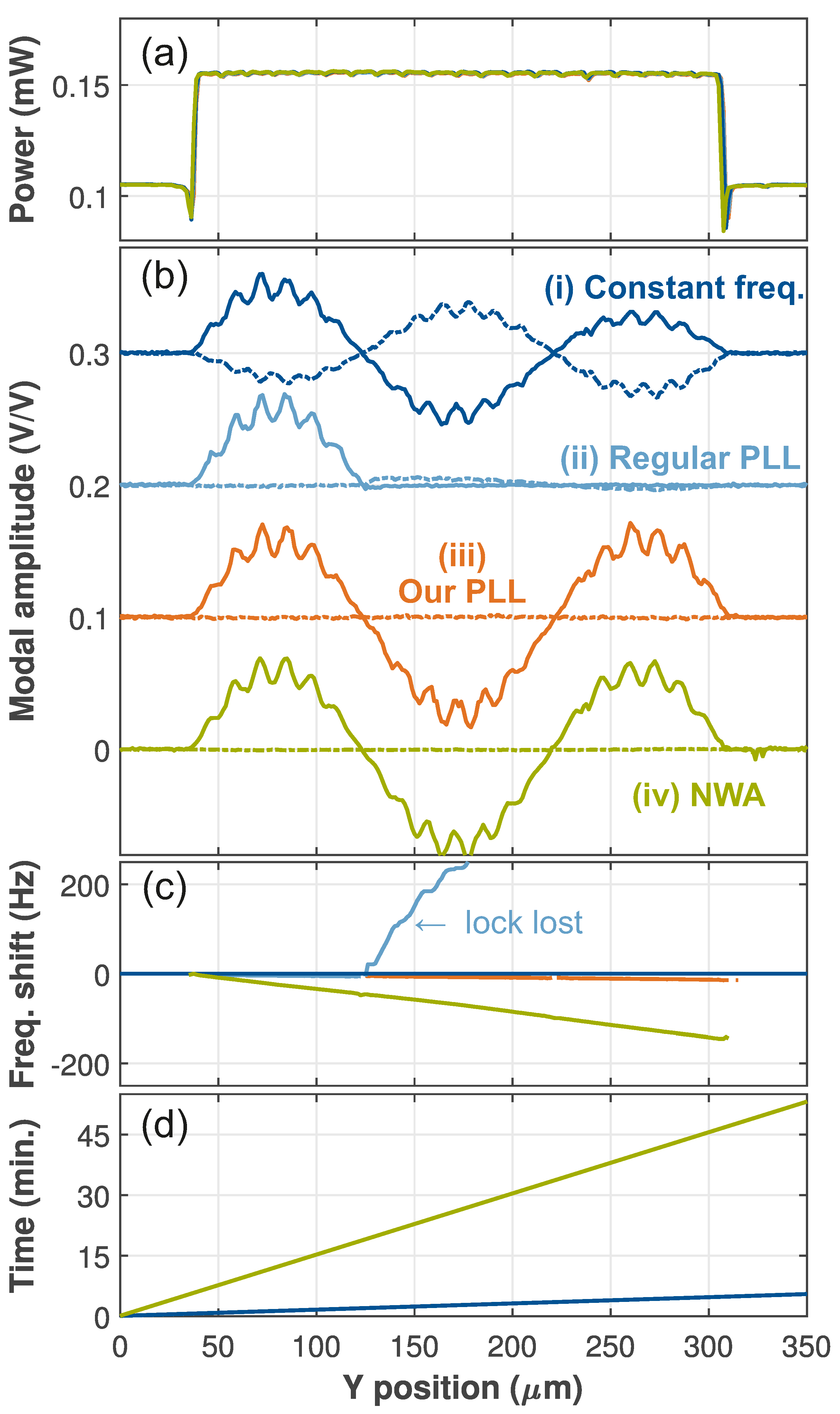
3.1. Comparison of Different Methods
3.2. 2D Mode Maps
4. Conclusions
Author Contributions
Funding
Acknowledgments
Conflicts of Interest
Appendix A. Demodulation, Response, and Mode Shape
Appendix A.1. Excitation and Detection
Appendix A.2. Demodulation
Appendix A.3. Response and Mode Shape
Appendix A.4. Harmonic Oscillator Response
Appendix B. Mode Properties

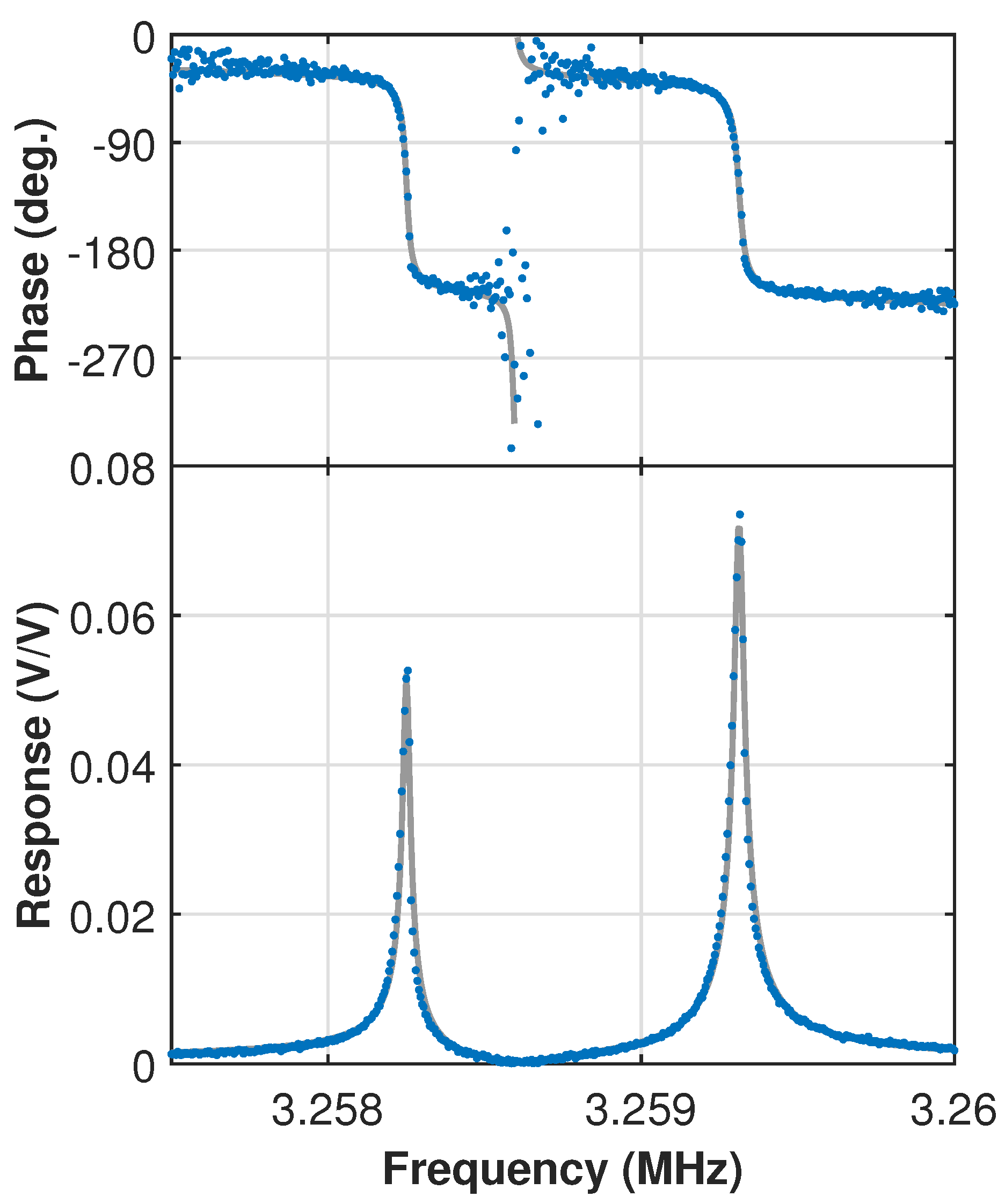
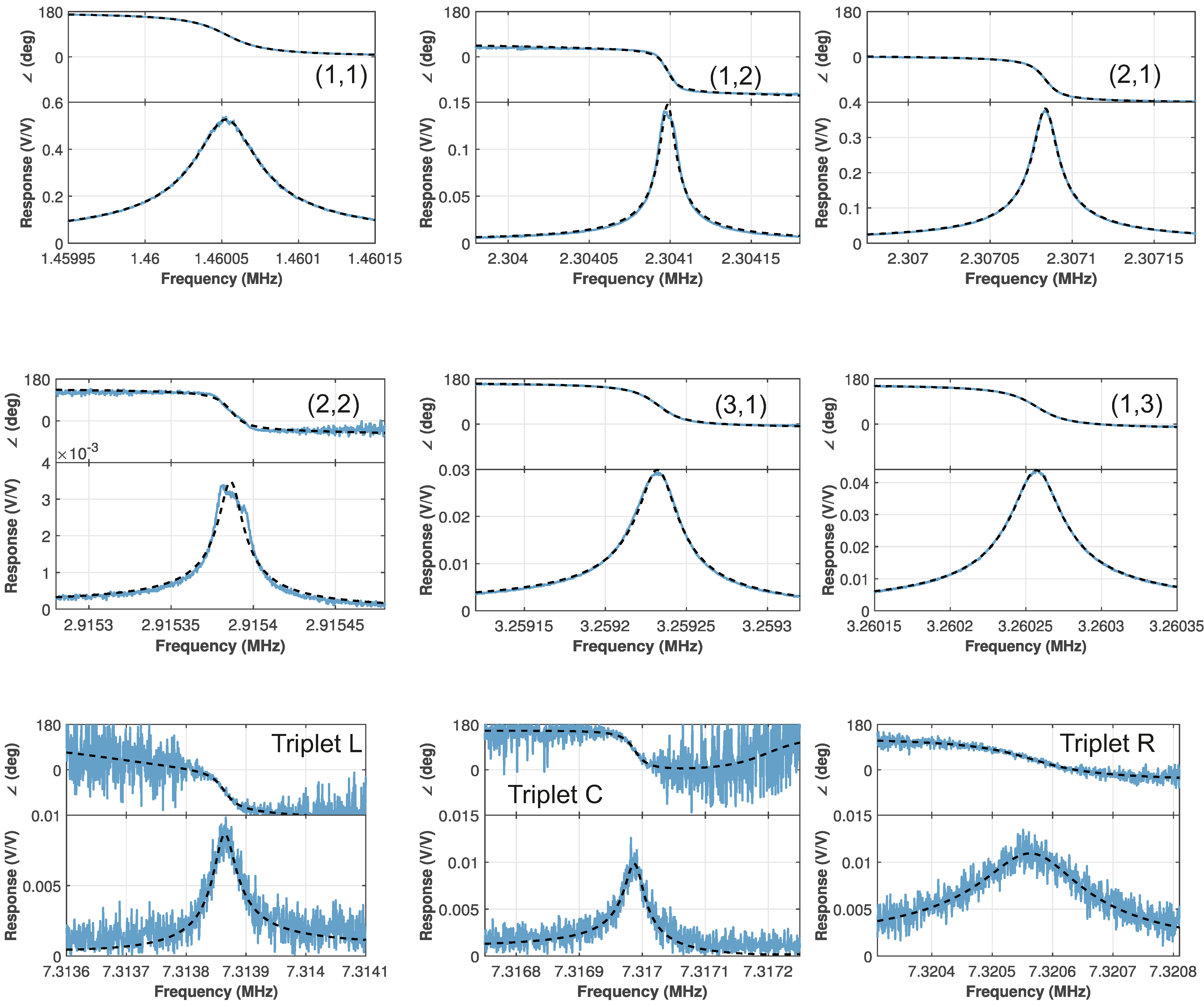
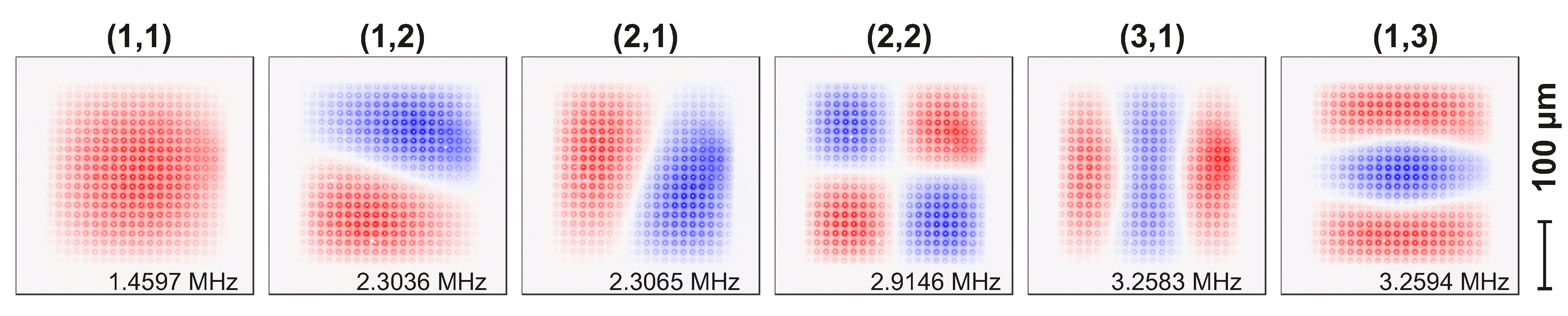
| Mode | Excitation | Frequency | Q | ||||
|---|---|---|---|---|---|---|---|
| (dBm) | (MHz) | () | (Hz) | (V/V) | (rad) | (°) | |
| (1,1) | −45 | 1.460053 | 87 | ||||
| (1,2) | −50 | 2.304098 | −68 | ||||
| (2,1) | −50 | 2.307084 | −98 | ||||
| (2,2) | −35 | 2.915386 | −104 | ||||
| (3,1) | −35 | 3.259232 | −111 | ||||
| (1,3) | −40 | 3.260257 | −20 | ||||
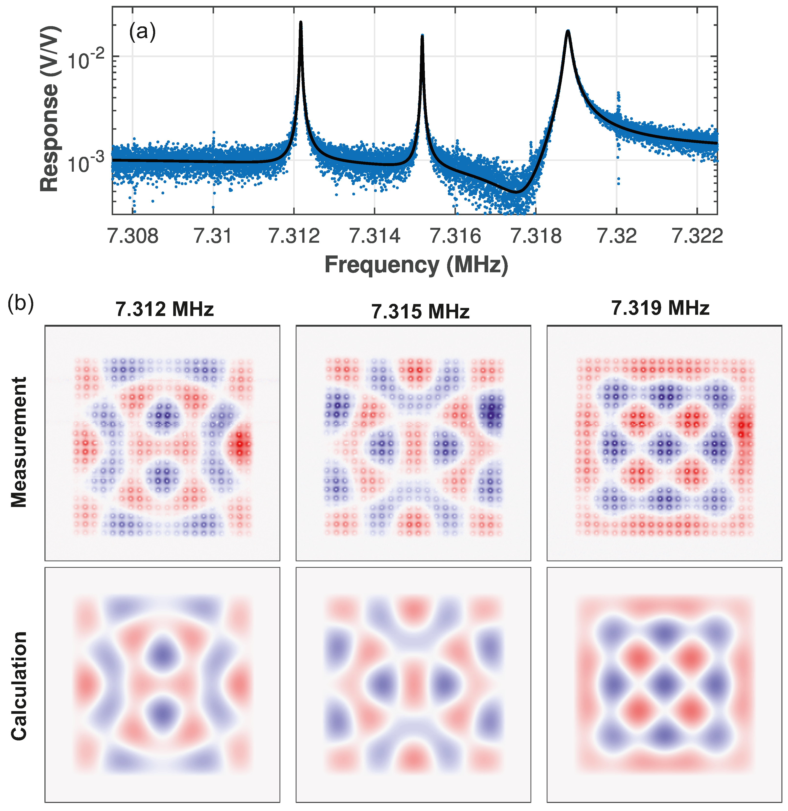
| Triplet L | −35 | 7.313864 | −68.8 | ||||
| Triplet C | −35 | 7.316988 | −263.3 | ||||
| Triplet R | −35 | 7.320566 | 49.8 |
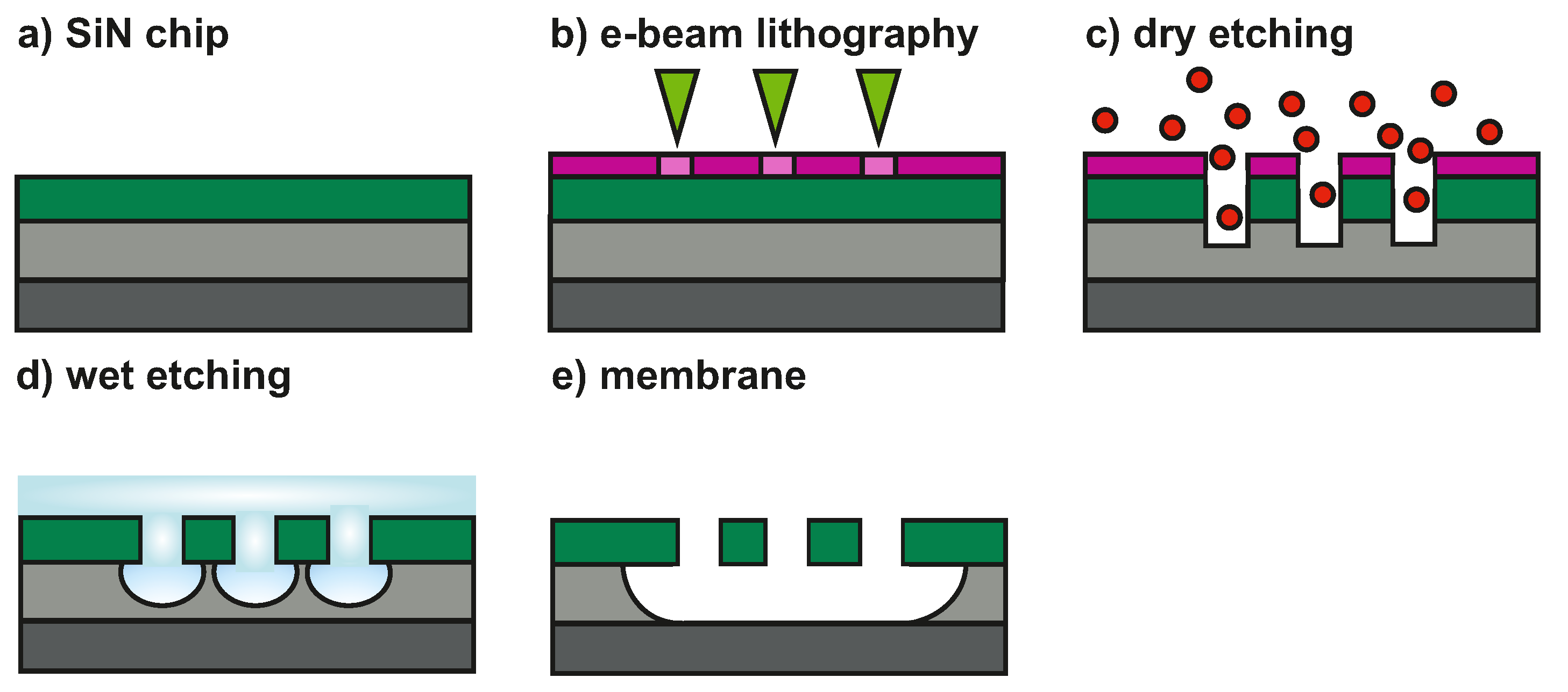
Appendix C. Sample Fabrication
References
- Hesjedal, T.; Chilla, E.; Fröhlich, H.J. High resolution visualization of acoustic wave fields within surface acoustic wave devices. Appl. Phys. Lett. 1997, 70, 1372–1374. [Google Scholar] [CrossRef]
- Venkatasubramanian, A.; Sauer, V.T.K.; Roy, S.K.; Xia, M.; Wishart, D.S.; Hiebert, W.K. Nano-Optomechanical Systems for Gas Chromatography. Nano Lett. 2016, 16, 6975–6981. [Google Scholar] [CrossRef]
- Naik, A.K.; Hanay, M.S.; Hiebert, W.K.; Feng, X.L.; Roukes, M.L. Towards single-molecule nanomechanical mass spectrometry. Nat. Nano 2009, 4, 445–450. [Google Scholar] [CrossRef]
- McKeown, S.J.; Wang, X.; Yu, X.; Goddard, L.L. Realization of palladium-based optomechanical cantilever hydrogen sensor. Microsyst. Nanoneng. 2017, 3. [Google Scholar] [CrossRef] [PubMed] [Green Version]
- Melcher, J.; Stirling, J.; Cervantes, F.G.; Pratt, J.R.; Shaw, G.A. A self-calibrating optomechanical force sensor with femtonewton resolution. Appl. Phys. Lett. 2014, 105. [Google Scholar] [CrossRef] [Green Version]
- Bleszynski-Jayich, A.C.; Shanks, W.E.; Peaudecerf, B.; Ginossar, E.; von Oppen, F.; Glazman, L.; Harris, J.G.E. Persistent Currents in Normal Metal Rings. Science 2009, 326, 272–275. [Google Scholar] [CrossRef] [PubMed] [Green Version]
- Fong, K.Y.; Li, H.K.; Zhao, R.; Yang, S.; Wang, Y.; Zhang, X. Phonon heat transfer across a vacuum through quantum fluctuations. Nature 2019, 576, 243–247. [Google Scholar] [CrossRef] [PubMed]
- Singh, R.; Purdy, T.P. Detecting Acoustic Blackbody Radiation with an Optomechanical Antenna. Phys. Rev. Lett. 2020, 125, 120603. [Google Scholar] [CrossRef]
- LaHaye, M.D.; Buu, O.; Camarota, B.; Schwab, K.C. Approaching the Quantum Limit of a Nanomechanical Resonator. Science 2004, 304, 74–77. [Google Scholar] [CrossRef] [Green Version]
- Etaki, S.; Poot, M.; Mahboob, I.; Onomitsu, K.; Yamaguchi, H.; van der Zant, H.S.J. Motion detection of a micromechanical resonator embedded in a d.c. SQUID. Nat. Phys. 2008, 4, 785–788. [Google Scholar] [CrossRef] [Green Version]
- Anetsberger, G.; Arcizet, O.; Unterreithmeier, Q.P.; Riviere, R.; Schliesser, A.; Weig, E.M.; Kotthaus, J.P.; Kippenberg, T.J. Near-field cavity optomechanics with nanomechanical oscillators. Nat. Phys. 2009, 5, 909–914. [Google Scholar] [CrossRef] [Green Version]
- Barg, A.; Tsaturyan, Y.; Belhage, E.; Nielsen, W.H.P.; Møller, C.B.; Schliesser, A. Measuring and imaging nanomechanical motion with laser light. Appl. Phys. B 2016, 123, 8. [Google Scholar] [CrossRef] [PubMed] [Green Version]
- Zhang, X.; Waitz, R.; Yang, F.; Lutz, C.; Angelova, P.; Gölzhäuser, A.; Scheer, E. Vibrational modes of ultrathin carbon nanomembrane mechanical resonators. Appl. Phys. Lett. 2015, 106, 063107. [Google Scholar] [CrossRef] [Green Version]
- Davidovikj, D.; Slim, J.J.; Cartamil-Bueno, S.J.; van der Zant, H.S.J.; Steeneken, P.G.; Venstra, W.J. Visualizing the Motion of Graphene Nanodrums. Nano Lett. 2016, 16, 2768–2773. [Google Scholar] [CrossRef]
- Shen, Z.; Han, X.; Zou, C.L.; Tang, H.X. Phase sensitive imaging of 10 GHz vibrations in an AlN microdisk resonator. Rev. Sci. Instrum. 2017, 88. [Google Scholar] [CrossRef] [PubMed]
- Romero, E.; Kalra, R.; Mauranyapin, N.; Baker, C.; Meng, C.; Bowen, W. Propagation and Imaging of Mechanical Waves in a Highly Stressed Single-Mode Acoustic Waveguide. Phys. Rev. Appl. 2019, 11, 064035. [Google Scholar] [CrossRef] [Green Version]
- Garcia-Sanchez, D.; van der Zande, A.M.; Paulo, A.S.; Lassagne, B.; McEuen, P.L.; Bachtold, A. Imaging Mechanical Vibrations in Suspended Graphene Sheets. Nano Lett. 2008, 8, 1399–1403. [Google Scholar] [CrossRef] [Green Version]
- Garcia-Sanchez, D.; Paulo, A.S.; Esplandiu, M.J.; Perez-Murano, F.; Forró, L.; Aguasca, A.; Bachtold, A. Mechanical Detection of Carbon Nanotube Resonator Vibrations. Phys. Rev. Lett. 2007, 99, 085501. [Google Scholar] [CrossRef] [Green Version]
- Hoch, D.; Sommer, T.; Mueller, S.; Poot, M. On-chip quantum optics and integrated optomechanics. Turk. J. Phys. 2020, 44, 239–246. [Google Scholar] [CrossRef]
- Hoch, D.; Yao, X.; Poot, M. Geometric tuning of stress in silicon nitride beam resonators. Bull. Am. Phys. Soc. 2021. in preparation. [Google Scholar]
- Terrasanta, G.; Müller, M.; Sommer, T.; Geprägs, S.; Gross, R.; Althammer, M.; Poot, M. Growth of aluminum nitride on a silicon nitride substrate for hybrid photonic circuits. Mater. Quantum Technol. 2021, 1, 021002. [Google Scholar] [CrossRef]
- Adiga, V.P.; Ilic, B.; Barton, R.A.; Wilson-Rae, I.; Craighead, H.G.; Parpia, J.M. Modal dependence of dissipation in silicon nitride drum resonators. Appl. Phys. Lett. 2011, 99, 253103. [Google Scholar] [CrossRef] [Green Version]
- Strauss, W.A. Partial Differential Equations—An Introduction; John Wiley and Sons, Inc.: Hoboken, NJ, USA, 1992. [Google Scholar]
- Poot, M.; van der Zant, H.S. Mechanical systems in the quantum regime. Phys. Rep. 2012, 511, 273–335. [Google Scholar] [CrossRef] [Green Version]
- Lide, D.R. (Ed.) Handbook of Chemistry and Physics; CRC Press: Boca Raton, FL, USA, 1974. [Google Scholar]
- Miller, D.; Alemán, B. Spatially resolved optical excitation of mechanical modes in graphene NEMS. Appl. Phys. Lett. 2019, 115, 193102. [Google Scholar] [CrossRef] [Green Version]
- Rohse, P.; Butlewski, J.; Klein, F.; Wagner, T.; Friesen, C.; Schwarz, A.; Wiesendanger, R.; Sengstock, K.; Becker, C. A cavity optomechanical locking scheme based on the optical spring effect. Rev. Sci. Instrum. 2020, 91, 103102. [Google Scholar] [CrossRef]
- Poot, M.; Fong, K.Y.; Tang, H.X. Classical non-Gaussian state preparation through squeezing in an optoelectromechanical resonator. Phys. Rev. A 2014, 90, 063809. [Google Scholar] [CrossRef] [Green Version]
- Poot, M.; Fong, K.Y.; Tang, H.X. Deep feedback-stabilized parametric squeezing in an opto-electromechanical system. New J. Phys. 2015, 17, 043056. [Google Scholar] [CrossRef] [Green Version]
- Cole, G.D.; Wilson-Rae, I.; Werbach, K.; Vanner, M.R.; Aspelmeyer, M. Phonon-tunnelling dissipation in mechanical resonators. Nat. Commun. 2011, 2, 231. [Google Scholar] [CrossRef] [Green Version]
- Sun, X.; Zheng, J.; Poot, M.; Wong, C.W.; Tang, H.X. Femtogram Doubly Clamped Nanomechanical Resonators Embedded in a High-Q Two-Dimensional Photonic Crystal Nanocavity. Nano Lett. 2012, 12, 2299–2305. [Google Scholar] [CrossRef] [PubMed]
- Poot, M.; Etaki, S.; Yamaguchi, H.; van der Zant, H.S.J. Discrete-time quadrature feedback cooling of a radio-frequency mechanical resonator. Appl. Phys. Lett. 2011, 99, 013113. [Google Scholar] [CrossRef] [Green Version]
- Jhung, M.J.; Jeong, K.H. Free vibration analysis of perforated plate with square penetration pattern using equivalent material properties. Nucl. Eng. Technol. 2015, 47, 500–511. [Google Scholar] [CrossRef] [Green Version]
- Williams, K.; Muller, R. Etch rates for micromachining processing. J. Microelectromech. Syst. 1996, 5, 256–269. [Google Scholar] [CrossRef]

Publisher’s Note: MDPI stays neutral with regard to jurisdictional claims in published maps and institutional affiliations. |
© 2021 by the authors. Licensee MDPI, Basel, Switzerland. This article is an open access article distributed under the terms and conditions of the Creative Commons Attribution (CC BY) license (https://creativecommons.org/licenses/by/4.0/).
Share and Cite
Hoch, D.; Haas, K.-J.; Moller, L.; Sommer, T.; Soubelet, P.; Finley, J.J.; Poot, M. Efficient Optomechanical Mode-Shape Mapping of Micromechanical Devices. Micromachines 2021, 12, 880. https://doi.org/10.3390/mi12080880
Hoch D, Haas K-J, Moller L, Sommer T, Soubelet P, Finley JJ, Poot M. Efficient Optomechanical Mode-Shape Mapping of Micromechanical Devices. Micromachines. 2021; 12(8):880. https://doi.org/10.3390/mi12080880
Chicago/Turabian StyleHoch, David, Kevin-Jeremy Haas, Leopold Moller, Timo Sommer, Pedro Soubelet, Jonathan J. Finley, and Menno Poot. 2021. "Efficient Optomechanical Mode-Shape Mapping of Micromechanical Devices" Micromachines 12, no. 8: 880. https://doi.org/10.3390/mi12080880
APA StyleHoch, D., Haas, K.-J., Moller, L., Sommer, T., Soubelet, P., Finley, J. J., & Poot, M. (2021). Efficient Optomechanical Mode-Shape Mapping of Micromechanical Devices. Micromachines, 12(8), 880. https://doi.org/10.3390/mi12080880