
Optimal Method for Test and Repair Memories Using Redundancy Mechanism for SoC


Abstract
:1. Introduction
- Implementation of BIST for critical testing by using the proposed March algorithm to improve a product’s quality. This memory BIST finds the faults and types in the memory to improve the fault coverage.
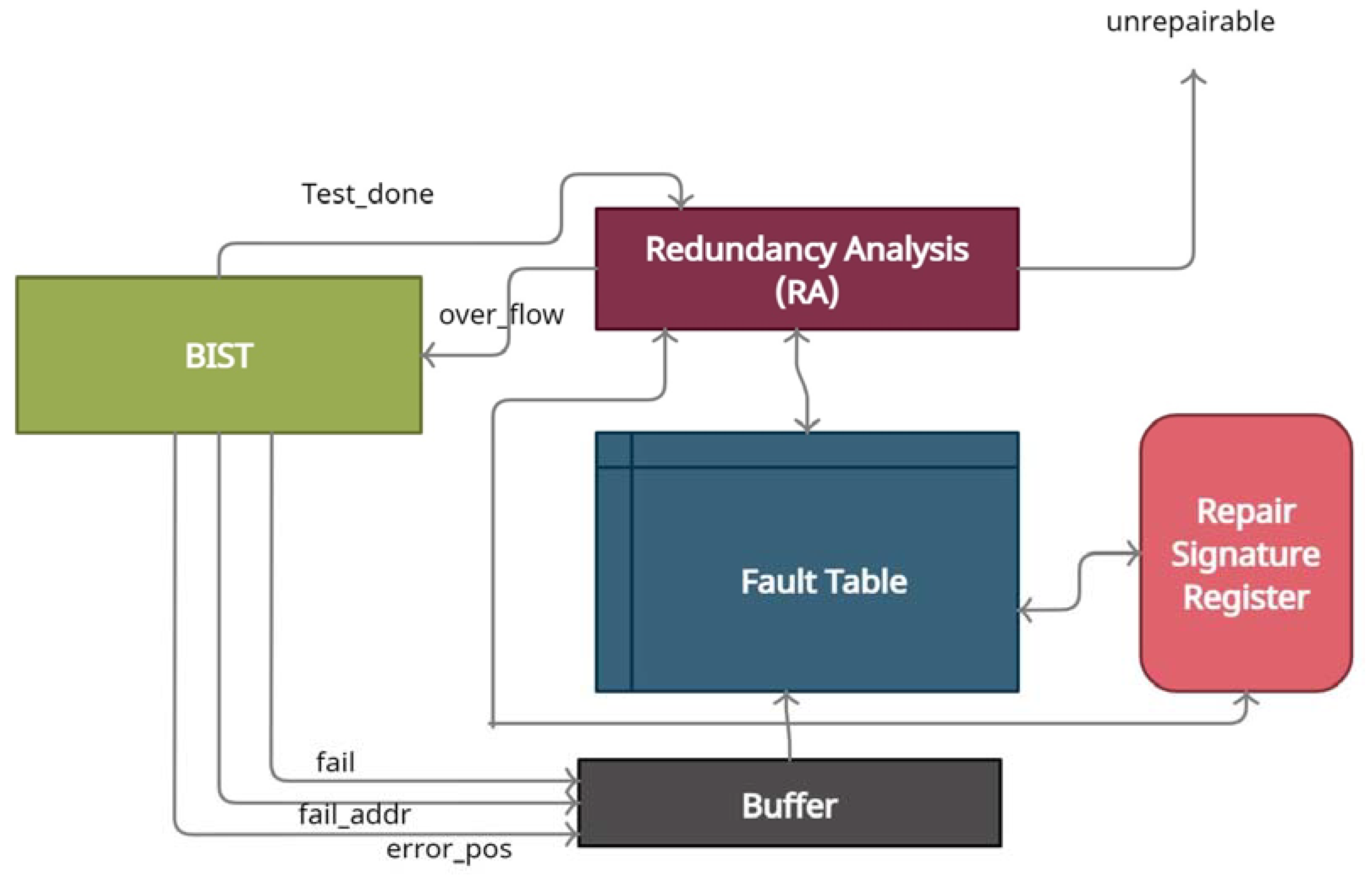
- A time- and cost-effective BISR solution to repair the faulty cells of the memory under test (MUT). The BIST controller generates the fault cells’ information to use spare memory. The BISR block performed the replacement of the faulty cells by redundant blocks, which are fault-free.
2. Proposed Architecture
2.1. Fault Testing
2.1.1. Proposed Algorithm
sift4:↑ (r1, w0); sift5: ↓ (r0, w0, r0); sift6: ↑ (r0, w1, r1); sift7: ↕ (r1);}
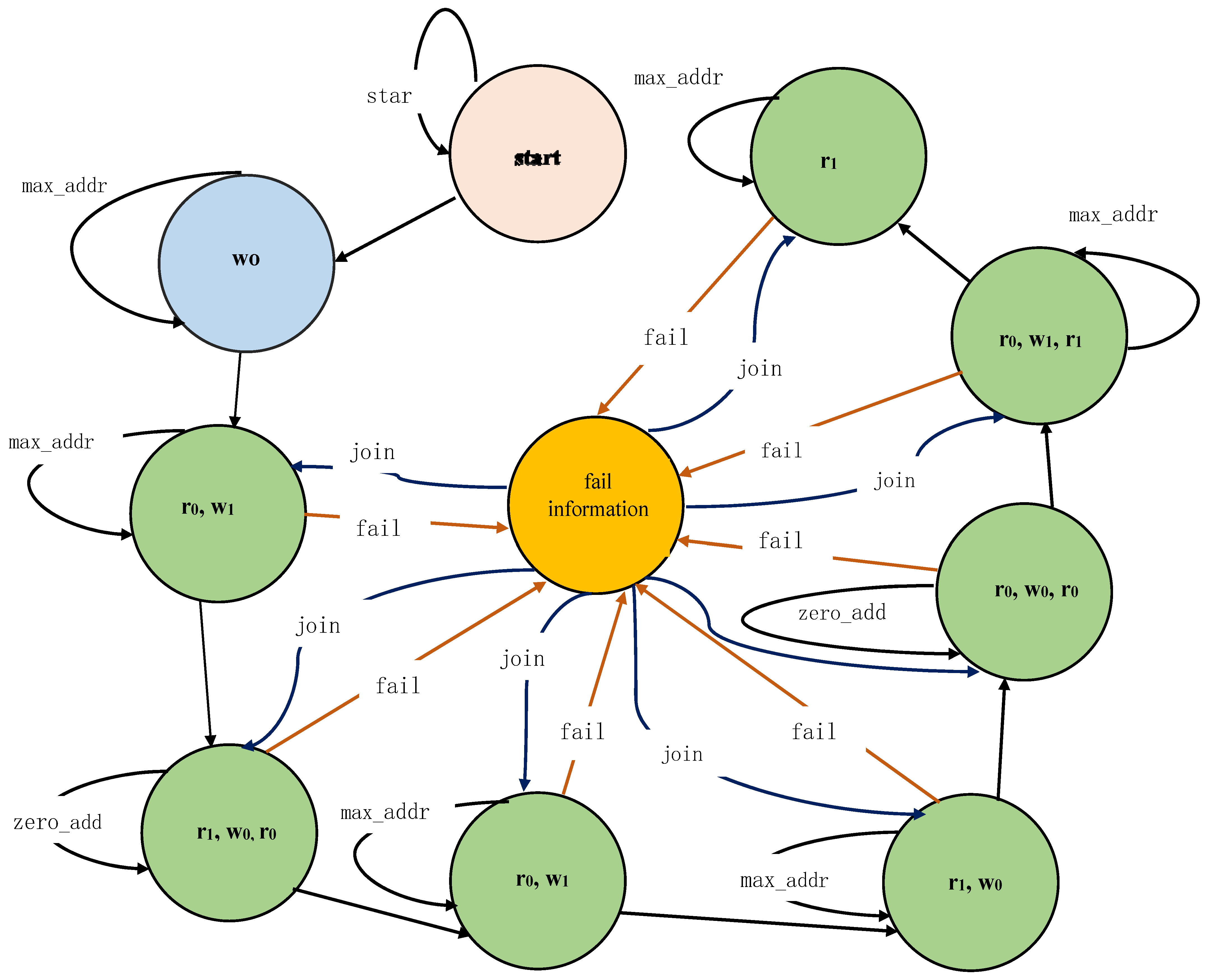
2.1.2. Memory BIST Controller
2.2. Fault Repair
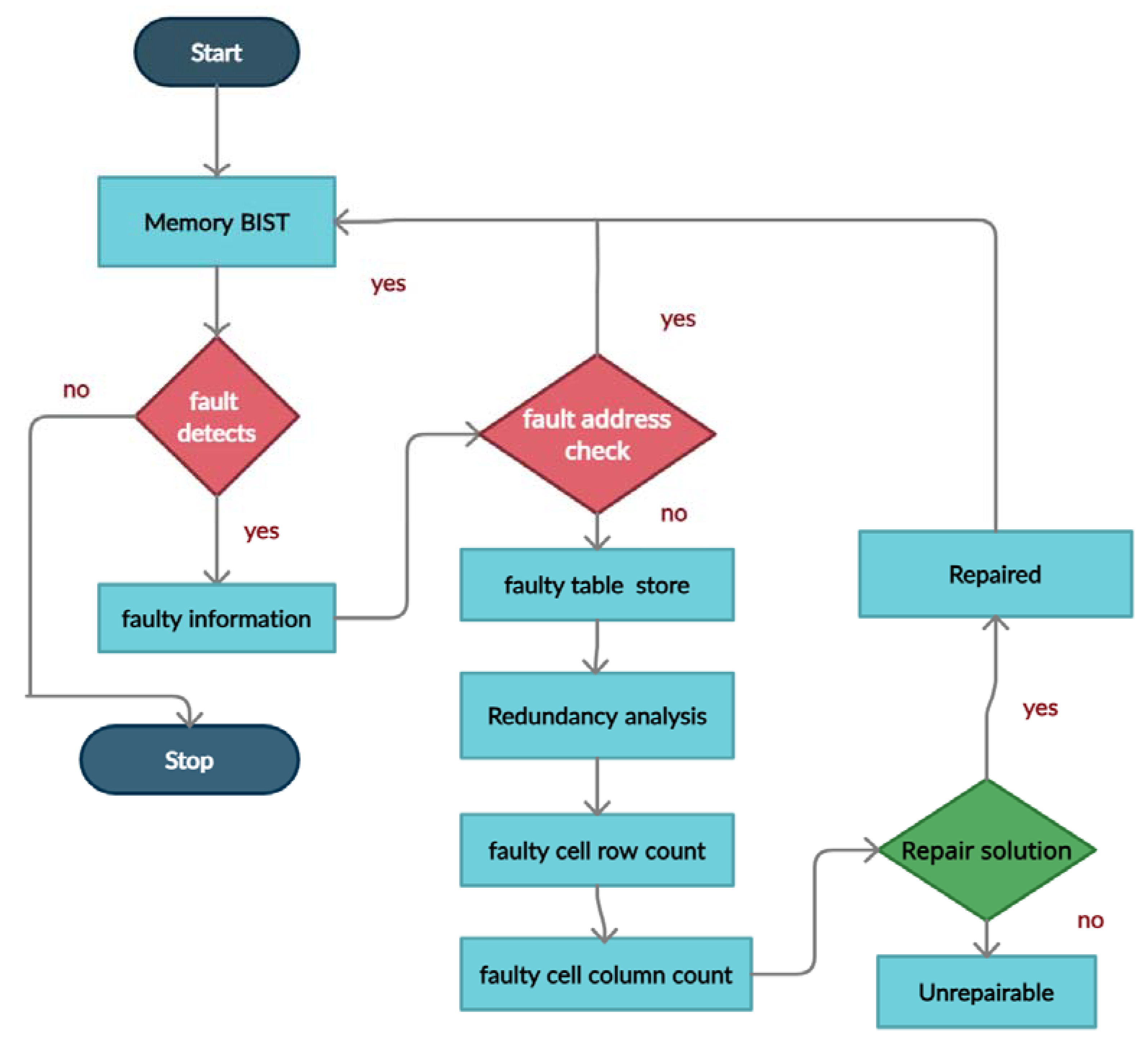
- The memory BIST block tests the MUT for faults. If fault detects, the BIST generates the failure information, and if no defects, the BIST stops.
- Once the BIST programs failure information, the repair process starts. The RA block reads the faulty addresses and compares them with the addresses previously available in the fault table. If an address is not previously known, it stores it into the fault table; otherwise, it ignores it.
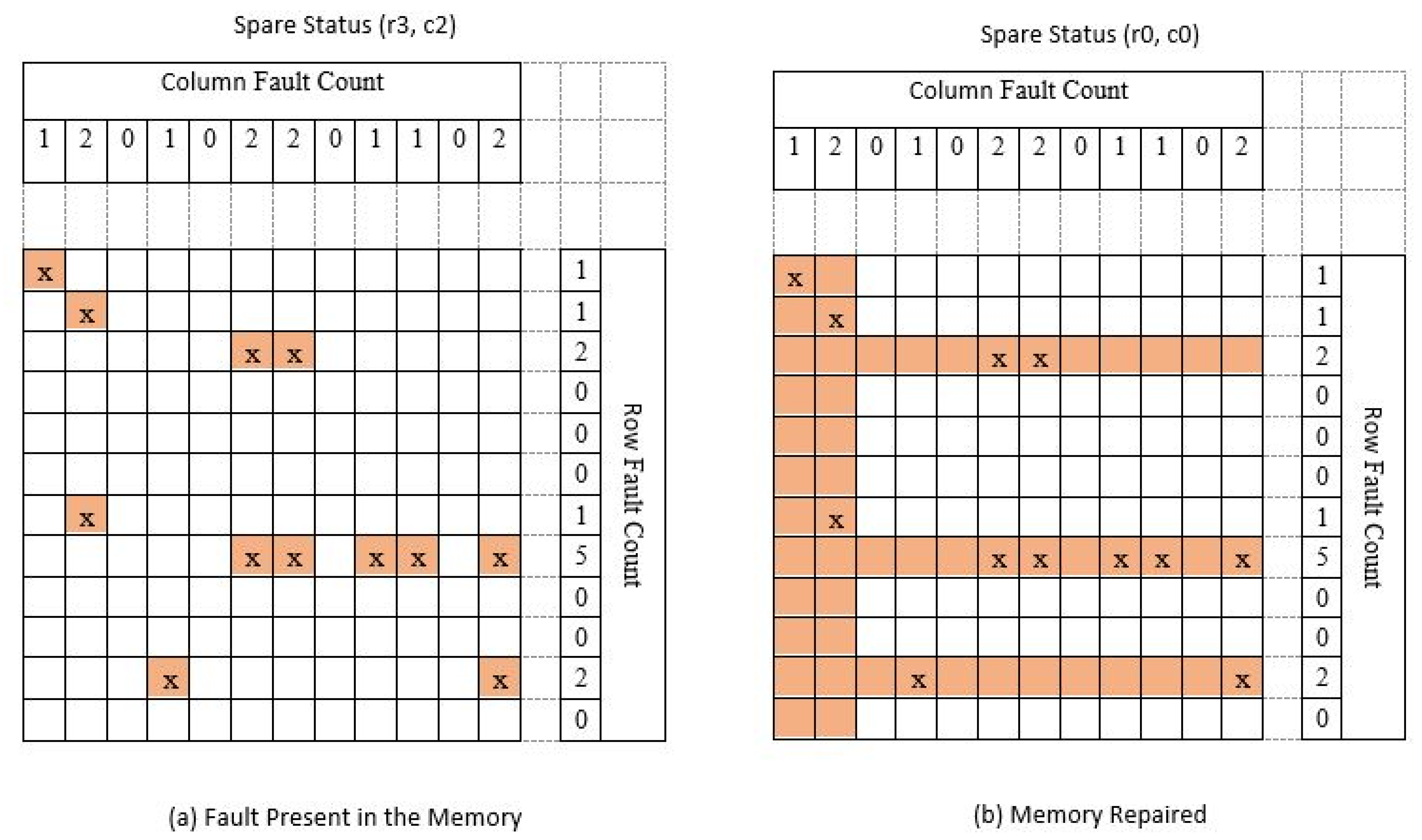
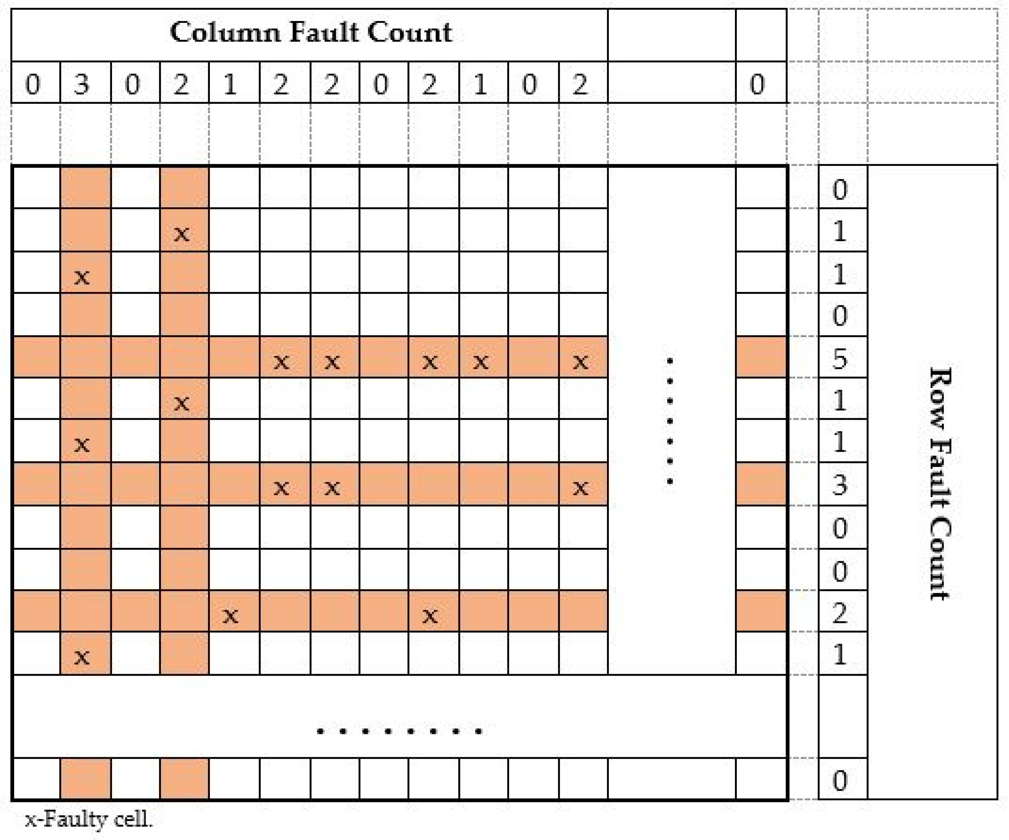
- Depending on the erroneous information, the RA performs a repair strategy and calculates fault count in a faulty row and faulty column.
- The repair signature is prepared based on the repair strategy and will store in the signature register.
- For whichever is higher, the row-defect count or column-defect count, it will allocate first and repeat until it reaches one fault in a particular row or particular column.
- If the row fault count equals the column fault count, the spare row will assign.
- If there is only one faulty cell that remains, the spare row allocates.
- The repair solution is provided for the memory under test whether the fault is repairable or unrepairable. In the case of multiple memories, the same BISR block will share within the numerous memories by selecting one after another.
3. Results and Comparison
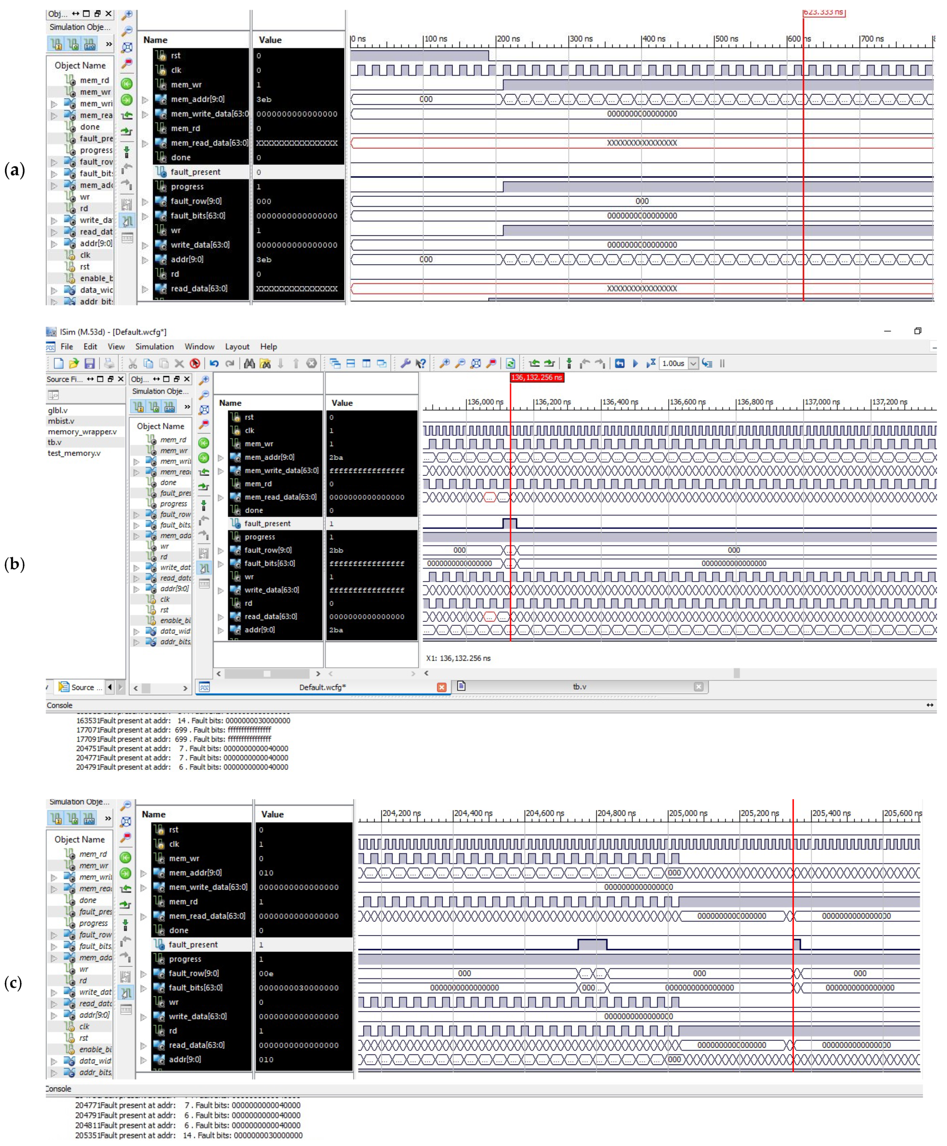
3.1. Functional Test
3.2. Synthesis Process
3.2.1. FPGA Synthesis
3.2.2. ASIC Synthesis
4. Discussion
5. Conclusions
Author Contributions
Funding
Data Availability Statement
Conflicts of Interest
References
- Du, X.; Reddy, S.M.; Cheng, W.-T.; Rayhawk, J.; Mukherjee, N. At-speed built-in self-repair analyzer for embedded word-oriented memories. In Proceedings of the 17th International Conference on VLSI Design, Mumbai, India, 9 January 2004. [Google Scholar]
- Cheng, W.-T.; Hill, C.; Kebichi, O. Full-Speed Bist Controller for Testing Embedded Synchronous Memories. U.S. Patent Application No. US 2005/0066247 A1, 24 March 2005. [Google Scholar]
- Semico Research Corp., Semico: System(s)-on-a-Chip–A Braver New World. Semico Research. 2015. Available online: https://semico.com/content/semico-systems-chip-%E2%80%93-braver-new-world (accessed on 9 July 2021).
- Zhang, G.; Yuan, Y.; Liang, F.; Wei, S.; Yang, C.-F. Low Cost Test Pattern Generation in Scan-Based BIST Schemes. Electronics 2019, 8, 314. [Google Scholar] [CrossRef] [Green Version]
- Peng, X.; Liu, R.; Yu, S. Optimizing Weight Mapping and Data Flow for Convolutional Neural Networks on Processing-in-Memory Architectures. IEEE Trans. Circuits Syst. I Regul. Pap. 2020, 67, 1333–1343. [Google Scholar] [CrossRef]
- Zhang, L.; Wang, Z.; Li, Y.; Mao, L. A Precise Design for Testing High-Speed Embedded Memory using a BIST Circuit. IETE J. Res. 2017, 63, 473–481. [Google Scholar] [CrossRef]
- Adams, R.D. High Performance Memory Testing: Design Principle, Fault Modeling and Self-Test; Springer: New York, NY, USA, 2003; pp. 149–172. [Google Scholar]
- Wojciechowski, A.A.; Marcinek, K.; Pleskacz, W.A. Configurable MBIST Processor for Embedded Memories Testing. In Proceedings of the 2019 MIXDES-26th International Conference “Mixed Design of Integrated Circuits and Systems”, Rzeszow, Poland, 27–29 June 2019. [Google Scholar]
- Chong, B.; Zhang, S. Algorithm-based fault tolerance for discrete wavelet transform implemented on GPUs. J. Syst. Archit. 2020, 108, 101823. [Google Scholar]
- Hantos, G.; Flynn, D.; Desmulliez, M.P.Y. Built-In Self-Test (BIST) Methods for MEMS: A Review. Micromachines 2020, 12, 40. [Google Scholar] [CrossRef] [PubMed]
- Ahmed, M.A.; Abuagoub, A.M. MBIST Controller Based on March-ee Algorithm. J. Circuits Syst. Comput. 2020. [Google Scholar] [CrossRef]
- Becker, A. Short burst software transparent on-line MBIST. In Proceedings of the 2016 IEEE 34th VLSI Test Symposium (VTS), Las Vegas, NV, USA, 25–27 April 2016; pp. 1–6. [Google Scholar] [CrossRef]
- Balaji, G.N.; Pandian, S.C. Design of test pattern generator (TPG) by an optimized low power design for testability (DFT) for scan BIST circuits using transmission gates. Clust. Comput. 2018, 22, 15231–15244. [Google Scholar] [CrossRef]
- Jamal, K.; Chari, K.M.; Srihari, P. Test pattern generation using thermometer code counter in TPC technique for BIST implementation. Microprocess. Microsyst. 2019, 71, 102890. [Google Scholar] [CrossRef]
- Chen, T.-J.; Li, J.-F.; Tseng, T.-W. Cost-Efficient Built-In Redundancy Analysis with Optimal Repair Rate for Word-Oriented RAMs. IEEE Trans. Comput. Aided Des. Integr. Circuits Syst. 2012, 31, 930–940. [Google Scholar] [CrossRef]
- Kang, W.; Lee, C.; Lim, H.; Kang, S. Optimized Built-In Self-Repair for Multiple Memories. IEEE Trans. Very Large Scale Integr. (VLSI) Syst. 2016, 24, 2174–2183. [Google Scholar] [CrossRef]
- Gopalan, K.; Pothiraj, S. A saboteur and mutant based built-in self-test and counting threshold-based built-in self repairing mechanism for memories. J. Ambient. Intell. Humaniz. Comput. 2020, 12, 6651–6663. [Google Scholar] [CrossRef]
- Lee, H.; Han, D.; Lee, S.; Kang, S. Dynamic Built-In Redundancy Analysis for Memory Repair. IEEE Trans. Very Large Scale Integr. (VLSI) Syst. 2019, 27, 2365–2374. [Google Scholar] [CrossRef]
- Zorian, Y.; Shoukourian, S. Embedded-memory test and repair: Infrastructure IP for SoC yield. IEEE Des. Test Comput. 2003, 20, 58–66. [Google Scholar] [CrossRef]
- Tseng, Y.-P.; Wang, V.; Chen, L.; Liu, A.-H. Method and System for Performing Memory Repair Analysis. U.S. Patent US 20030097626 A1, 22 May 2003. [Google Scholar]
- Kim, S.; Chu, H.; Yang, I.; Hong, S.; Jung, S.H.; Cho, K.-H. A Hierarchical Self-Repairing Architecture for Fast. IEEE Trans. Very Large Scale Integr. (VLSI) Syst. 2012, 20. [Google Scholar] [CrossRef]
- Hamdioui, S.; Van De Goor, A.; Rodgers, M. March SS: A test for all static simple RAM faults. In Proceedings of the 2002 IEEE International Workshop on Memory Technology, Design and Testing (MTDT2002), Bendor, France, 12 July 2002; pp. 95–100. [Google Scholar]
- Caşcaval, P.; Caşcaval, D. March test algorithm for unlinked static reduced three-cell coupling faults in random-access memories. Microelectron. J. 2019, 93, 104619. [Google Scholar] [CrossRef]
- Wang, L.-T.; Wu, C.-W.; Wen, X. Memory Testing and Built-In Self-Test. In VLSI Test Principles and Architectures, 1st ed.; Design for Testability; Elsevier: Amsterdam, The Netherlands, 2006. [Google Scholar]
- Wang, Y.; Zheng, Q.; Yuan, Y. The Improvement of March C+ Algorithm for Embedded Memory Test. Commun. Comput. Inf. Sci. 2016, 31–37. [Google Scholar] [CrossRef]
- Cho, K.; Cho, H.; Lee, C.; Kang, S. A survey of repair analysis algo-rithms for memories. ACM Comput. Surv. 2016, 49. [Google Scholar] [CrossRef]
- Ahmed, M.A.; Abubaker, E.M.; Eljialy, S.A. Memory test and repair technique for SoC based devices. IEICE Electron. Express 2021, 18, 20210092. [Google Scholar] [CrossRef]


| March-Sift Algorithm | ||
|---|---|---|
| act on all memory locations(ml), any address order ascending or descending | sift0: ↕ (w0); | |
| for a := 0 to h do | start from first (0) to last (h) address (a); | |
| write 0 to ml[a]; | write 0 to memory location (ml) | |
| end; | ||
| act on all memory locations (ml), in sequence ascending order | sift1: ↑ (r0, w1); | |
| for a := 0 to h do | start from first (0) to last (h) address (a) | |
| read ml[a]; | read ml and compare with expected value (0), if mismatch record the result | |
| write 1 to ml[a]; | write 1 to memory location (ml) | |
| end; | ||
| act on all memory locations (ml), in sequence descending order | sift2: ↓ (r1, w0, r0); | |
| for a := h down to 0 do | start from last (h) to first (0) address (a) | |
| read ml[a]; | read ml and compare with expected value (1), if mismatch record the result | |
| write 0 to ml[a]; | write 0 to memory location (ml) | |
| read ml[a]; | read ml and compare with expected value (0), if mismatch record the result | |
| end; | ||
| act on all memory locations (ml), in sequence ascending order | sift3: ↑ (r0, w1); | |
| for a := 0 to h do | start from first (0) to last (h) address (a) | |
| read ml[a]; | read ml and compare with expected value (0), if mismatch record the result | |
| write 1 to ml[a]; | write 1 to memory location (ml) | |
| end; | ||
| act on all memory locations (ml), in sequence ascending order | sift4: ↑ (r1, w0); | |
| for a := 0 down to h do | start from first (0) to last (h) address (a) | |
| read ml[a]; | read ml and compare with expected value (1), if mismatch record the result | |
| write 0 to ml[a]; | write 0 to memory location (ml) | |
| read ml[a]; | read ml and compare with expected value (0), if mismatch record the result | |
| end; | ||
| act on all memory locations (ml), in sequence descending order | sift5: ↓ (r0, w0, r0); | |
| for a := h to 0 do | start from last (h) to first (0) address (a); | |
| read ml[a]; | read ml and compare with expected value (0), if mismatch record the result | |
| write 0 to ml[a]; | write 0 to memory location (ml) | |
| read ml[a]; | read ml and compare with expected value (0), if mismatch record the result | |
| end; | ||
| act on all memory locations (ml), in sequence ascending order | sift6: ↑ (r0, w1, r1); | |
| for a := 0 down to h do | start from first (0) to last (h) address (a) | |
| read ml[a]; | read ml and compare with expected value (0), if mismatch record the result | |
| write 1 to ml[a]; | write 1 to memory location (ml) | |
| read ml[a]; | read ml and compare with expected value (1), if mismatch record the result | |
| end; | ||
| act on all memory locations (ml), in sequence ascending order | sift7: ↕ (r1); | |
| for a := 0 to h do | start from first (0) to last (h) address (a) | |
| read ml[a]; | read ml and compare with expected value (1), if mismatch record the result | |
| end; | ||
| Faulty Addresses | Read Data with Faulty Bits | Fault-Type Detection |
|---|---|---|
| Case I NPSF | ||
| 0 | 0000000000000000 | No fault |
| 6 | 0000000000040000 | NPSF at cell 18 |
| 7 | 0000000000040000 | NPSF at cell 18 |
| Case II Stuck-at-0 Faults | ||
| 8 | ffff fffe ffff ffff | Stuck-at-0 fault at cell 32 |
| 18 | ffff ffff ffff 3fff | Stuck-at-0 fault at cell 12–13 |
| Case III Stuck-at-1 Faults | ||
| 22 | 0000000070000000 | Stuck-at-1 fault at cell 28–29 |
| 58 | 0000000000000300 | Stuck-at-1 fault at cell 8–9 |
| 109 | 0001000000000000 | Stuck-at-1 fault at cell 48 |
| Case IV transition faults and address decoder faults | ||
| 120 | 0000000000000000 | No fault |
| 127 | 0000000000004000 | Transition fault at 14 |
| 367 | ffff ffff fffb ffff | Transition fault at 17 |
| 455 | 0000000001000000 | Transition fault at 24 |
| 495 | null | Address Decoder fault will write to location 511 |
| 511 | ffff ffff ffff ffff | Address Decoder fault |
| 511 | 0000000000000000 | Overwrite |
| Case IV coupling faults | ||
| 699 | 0000000000000000 | No fault |
| 723 | 0000000000000000 | Coupled with cell 14 at location 1009 |
| 786 | ffff ffff ffff fff7 | Coupling fault at cell 4 with cell 5 at location 723 |
| 820 | ffff ffff ffff dfff | Cell 14 Coupled with a cell 56 of location 699 |
| Case V Write disturb faults (WDFs) | ||
| 887 | 0000000000000010 | Write ‘0’ but Cell 5 become ‘1’ |
| 967 | ffff ffff ffff efff | Write ‘1’ but Cell 13 become ‘0’ |
| Case VI Read disturb faults (RDFs) | ||
| 994 | 0001000000000000 | Read ‘0’ but Cell 49 become ‘1’ |
| 1009 | ffff ffff 7fff ffff | Read ‘1’ but Cell 32 become ‘0’ |
| Case VII Deceptive read destructive Faults (DRDFs) | ||
| 1012 | 0000000000400000 | Read ‘0’ it returns ‘0’ but cell become ‘1’ this appears in the next consecutive read at cell 23. |
| 1019 | ffff ffff fffdffff | Read ‘1’ it returns ‘1’ but cell become ‘0’ will appear in next consecutive read. |
| Test | March Elements | Fault Coverage | Features |
|---|---|---|---|
| March [22] | {c(w0); ⇑ (r0, w1, w0, w1); ⇑ (r1, w0, w1); ⇓ (r1, w0, w1, w0); ⇓ (r0, w1, w0)} | SAF, TF, ADF, some CFs | Complex with Moderate fault coverage |
| March Test Algorithm [23] | c (w0); ⇑ (r0, w1, w1, r1); (r1, w0, w0, r0); ⇓ (r0, w1, w1, r1); (r1, w0, w0, r0); c (r0); | SAF, TF, ADF, some CFs | Complex with reasonable fault coverage |
| March C [24] | {c(w0); ⇑ (r0, w1); ⇑ (r1, w0); ⇓ (r0, w1); ⇓ (r1, w0);c(r0)} | SAF, TF, ADF | Simple low fault coverage |
| March Y [25] | c (w0); ⇑ (r0, w1, r1); ⇑ (r1, w0, r0); ⇓ (r0, w1, r1); ⇓ (r1, w0, r0); c (r0); | SAF, TF, ADF, some CFs | Moderate and moderate fault coverage |
| Proposed March-sift | {↕ (w0); ↑ (r0, w1); ↓ (r1, w0, r0); ↑ (r0, w1); ↑ (r1, w0); ↓ (r0, w0, r0); ↑ (r0, w1, r1); ↕ (r1);} | SAF, TF, ADF, NPSF, CFs, WDFs, RDFs, DRDFs | Reasonable with Optimal fault coverage |
| Tool | Xilinx |
|---|---|
| Product Version | ISE 12.1 |
| Family | Virtex 6 |
| Target Device | xc6vlx75t-3ff484 |
| Package | FF484 |
| Speed | −3 |
| Logic Utilization | Used | Available | Utilization |
|---|---|---|---|
| Number of Slice Registers | 143 | 93,120 | 0% |
| Number of Slice LUTs | 253 | 46,560 | 0% |
| Number of fully used LUT-FF pairs | 139 | 220 | 69% |
| Number of bonded IOBs | 86 | 240 | 35% |
| Number of Block RAM/FIFO | 3 | 156 | 2% |
| Number of BUFG/BUFGCTRLs | 1 | 32 | 3% |
| Slice Logic Utilization | BIRA Chen [15] | BISR [16] | Counting Threshold (BISR) [17] | Proposed Method (BISR) |
|---|---|---|---|---|
| Number of Slice Registers | 343 | 295 | 188 | 143 |
| Number used as Flip Flops | 342 | 295 | 188 | 143 |
| Number of Slice LUTs | 409 | 387 | 287 | 253 |
| Number of occupied Slices | 176 | 156 | 70 | 59 |
| Number of LUT Flip; Flop pairs used | 227 | 201 | 165 | 107 |
| Number with an unused; Flip Flop | 207 | 186 | 73 | 80 |
| Number of RAM(8 K) (1024 × 64-bit dual-port RAM) | 4 | 4 | 2 | 3 |
| Timing Comparison | |||||
|---|---|---|---|---|---|
| March Algorithm | Minimum period ns | Minimum input arrival time before clock ns | Maximum output required time after clock ns | Maximum combinational path delay ns | Maximum Frequency MHz |
| Proposed BISR | 3.622 | 2.218 | 0.567 | 1.63 | 276 |
| BISR [16] | 5.32 | 2.61 | 4.37 | 2.23 | 203 |
| Counting threshold (BISR) [17] | 4.641 | 2.042 | 4.04 | 1.97 | 215.450 |
| Cresta [26] | 6.239 | 4.13 | 5.396 | 3.93 | 160.279 |
| Cell Count | Proposed BISR |
|---|---|
| Hierarchical Cell Count | 5 |
| Hierarchical Port Count | 19 |
| Leaf Cell Count | 656 |
| Buf/Inv Cell Count | 209 |
| Buf Cell Count | 9 |
| Inv Cell Count | 193 |
| CT Buf/Inv Cell Count | 0 |
| Combinational Cell Count | 583 |
| Sequential Cell Count | 187 |
| Macro Count | 0 |
| Design | Area (Cell) | Frequency (MHz) | Power (µw) |
|---|---|---|---|
| BIRA Chen [15] | 2957 | 250 | 197.2497 (3.7087 × 10⁷ pW (leakage) and 73uW Dynamic) |
| BISR [16] | 2376 | 320 | 147.732 (3.0626 × 10⁷ pW (leakage) and 98uW Dynamic) |
| Counting threshold (BISR) [17] | 2002 | 320 | 97.2497 (2.787 × 10⁷ pW (leakage) and 69uW Dynamic) |
| Proposed Method BISR | 1861 | 350 | 109.8623 (2.5087 × 10⁷ pW (leakage) and 69uW Dynamic) |
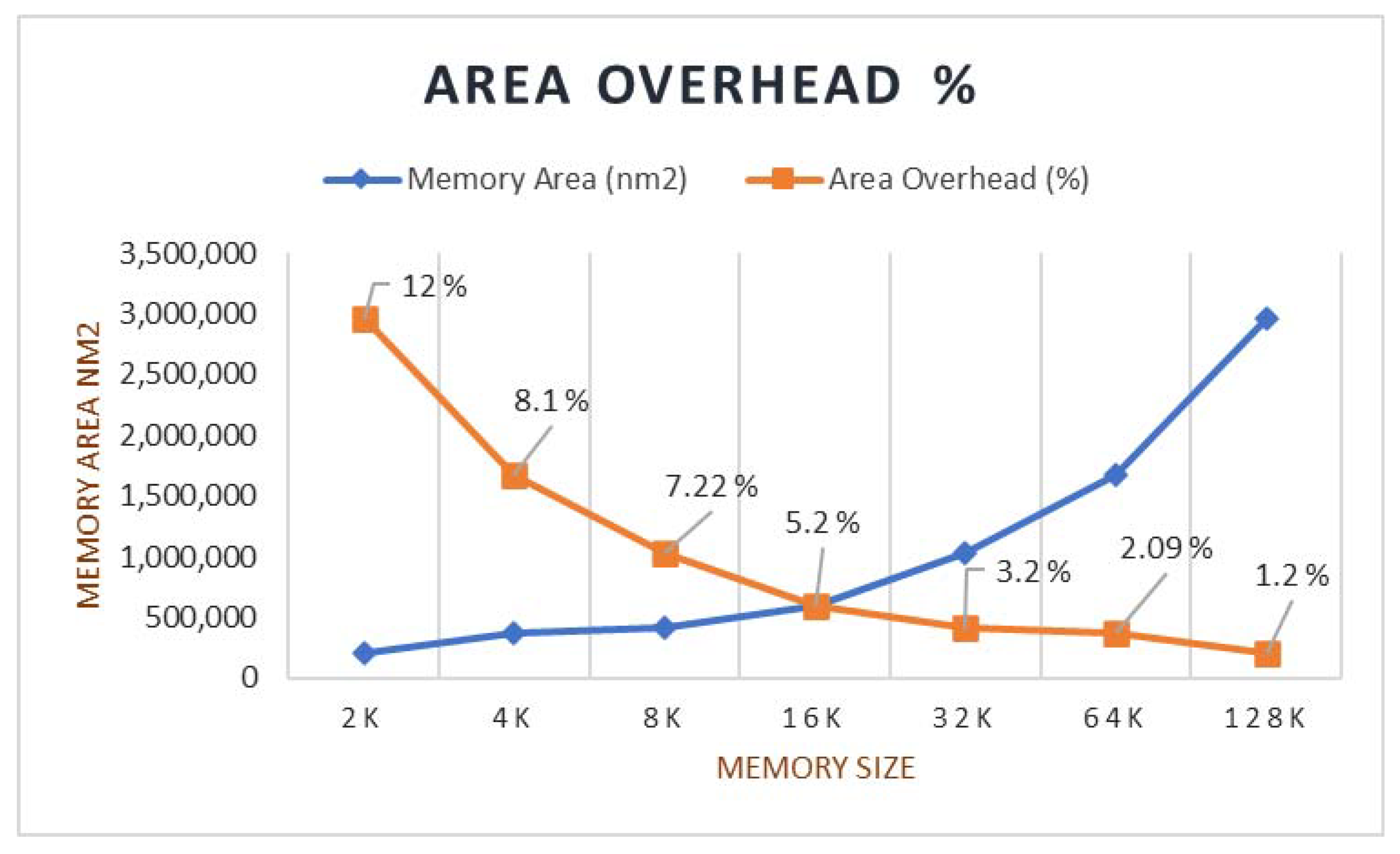
| Memory Size | Memory Area (nm2) | BISR (nm2) | Area Overhead (%) |
|---|---|---|---|
| 4 k | 367,095 | 29,932 | 8.1 |
| 8 k | 423,727 | 30,597 | 7.22 |
| 16 K | 603,137 | 31,756 | 5.2 |
| 32 k | 1,026,895 | 33,532 | 3.2 |
| 64 k | 1,673,452 | 34,527 | 2.09 |
| 128 k | 2,965,987 | 35,732 | 1.2 |
| Memory | BIRA Chen [15] | BISR [16] | Counting Threshold (BISR) [17] | Cresta [26] | Proposed Method BISR |
|---|---|---|---|---|---|
| Group 1 (8 k + 16 k) | 5.3 | 4.3 | 3.6 | 5.7 | 3.5 |
| Group 2 (32 k + 64 k) | 2.5 | 2.03 | 1.75 | 2.7 | 1.7 |
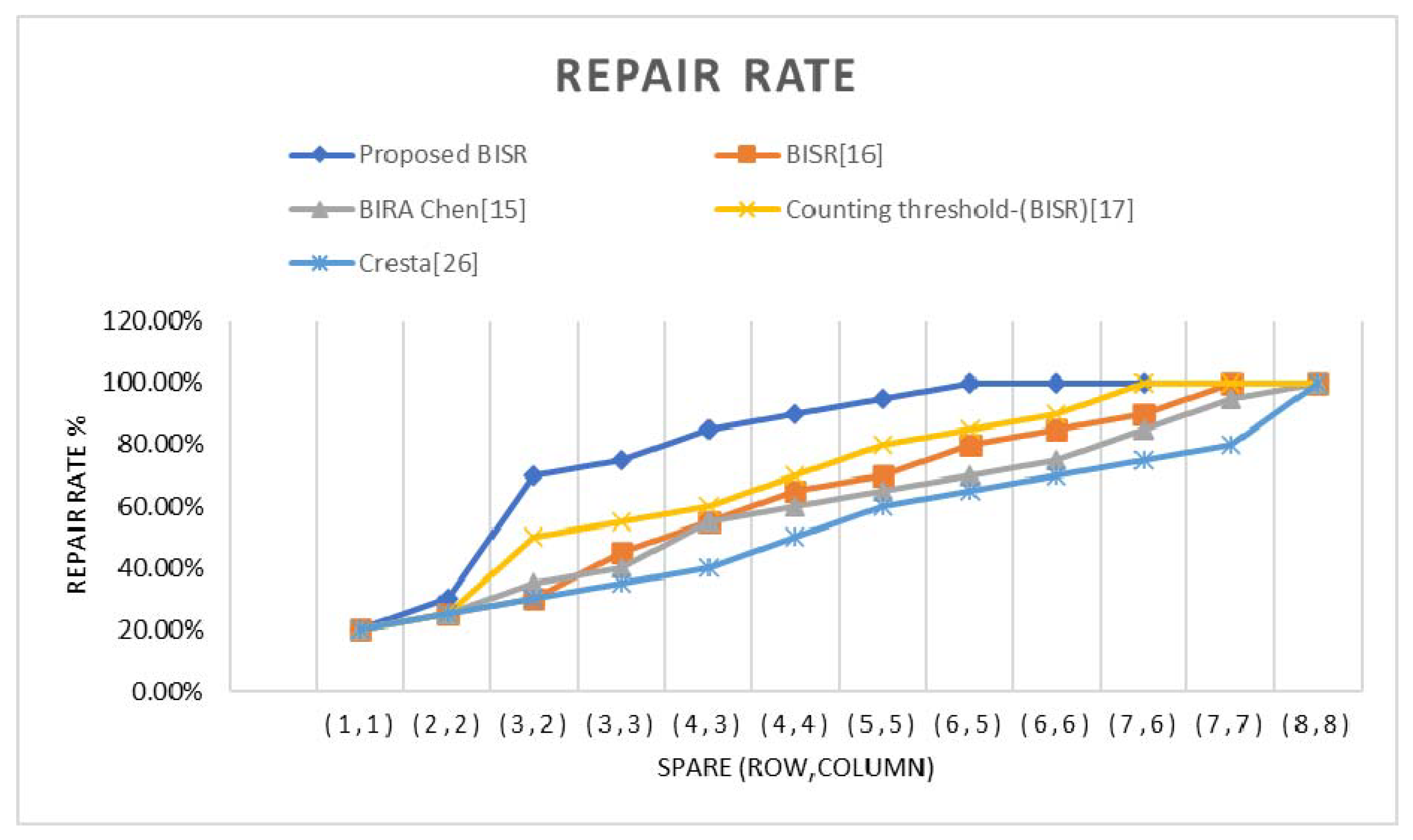
| BISR Approach | Repair Rate | Spare Allocation (Row, Column) | Memory Test Support (BIST) | Speed | Area Overhead |
|---|---|---|---|---|---|
| BIRA Chen [15] | High | High(variable) | Yes | Moderate | High |
| BISR [16] | High | High (3, 3) | Yes | Moderate | Moderate |
| Counting threshold (BISR) [17] | Low | High (3, 1) | No | Moderate | Moderate |
| Cresta [26] | High | Very High (3, 3) | No | Low | High |
| Proposed BISR | High | Low (3, 2) | Yes | High | Low |
Publisher’s Note: MDPI stays neutral with regard to jurisdictional claims in published maps and institutional affiliations. |
© 2021 by the authors. Licensee MDPI, Basel, Switzerland. This article is an open access article distributed under the terms and conditions of the Creative Commons Attribution (CC BY) license (https://creativecommons.org/licenses/by/4.0/).
Share and Cite
Alnatheer, S.; Ahmed, M.A. Optimal Method for Test and Repair Memories Using Redundancy Mechanism for SoC. Micromachines 2021, 12, 811. https://doi.org/10.3390/mi12070811
Alnatheer S, Ahmed MA. Optimal Method for Test and Repair Memories Using Redundancy Mechanism for SoC. Micromachines. 2021; 12(7):811. https://doi.org/10.3390/mi12070811
Chicago/Turabian StyleAlnatheer, Suleman, and Mohammed Altaf Ahmed. 2021. "Optimal Method for Test and Repair Memories Using Redundancy Mechanism for SoC" Micromachines 12, no. 7: 811. https://doi.org/10.3390/mi12070811
APA StyleAlnatheer, S., & Ahmed, M. A. (2021). Optimal Method for Test and Repair Memories Using Redundancy Mechanism for SoC. Micromachines, 12(7), 811. https://doi.org/10.3390/mi12070811