Article

Spin Polarization Properties of Two Dimensional GaP3 Induced by 3d Transition-Metal Doping

School of Physics and Electronics, Shandong Normal University, Jinan 250014, China
*
Authors to whom correspondence should be addressed.
These authors contributed equally to this paper.
Micromachines 2021, 12(7), 743; https://doi.org/10.3390/mi12070743
Submission received: 31 May 2021 / Revised: 22 June 2021 / Accepted: 23 June 2021 / Published: 24 June 2021

Abstract

:
The electronic structure and spin polarization properties of monolayer GaP3 induced by transition metal (TM) doping were investigated through a first-principles calculation based on density functional theory. The calculation results show that all the doped systems perform spin polarization properties, and the Fe–doped system shows the greatest spin polarization property with the biggest magnetic moment. Based on the analysis from the projected density of states, it was found that the new spin electronic states originated from the p–d orbital couplings between TM atoms and GaP3 lead to spin polarization. The spin polarization results were verified by calculating the spin density distributions and the charge transfer. It is effective to introduce the spin polarization in monolayer GaP3 by doping TM atoms, and our work provides theoretical calculation supports for the applications of triphosphide in spintronics.

1. Introduction

Since the discovery of graphene in 2004, two-dimensional (2D) materials have become an emerging class of materials. Compared with bulk materials, 2D materials are highly attractive for nanoelectronics, nanophotonics and spintronics at the nanoscale [1,2,3,4,5,6]. However, graphene has the shortcomings of zero band gap, which makes it unable to control the transport of carriers effectively and limits its development in some electronic fields. Beyond graphene, a series of 2D materials were experimentally stripped from the bulk crystals [7]. These 2D materials have their own advantages and disadvantages, for instance, hexagonal h-BN possesses a structure similar to graphene, but its wide band gap makes it an insulator, resulting in low overall carrier mobility [8,9,10]. As one of the typical 2D materials, transition metal di-chalcogenides (TMDCs) have the natural advantage of direct band gaps, controlled carrier mobility and suitable semiconductor band gaps, but this material’s oxidation resistance is very weak and can easily change under oxygen-containing conditions [11,12,13,14,15]. Besides, there are many other 2D materials, such as phosphorene [16,17,18], phosphide [19,20], Mxenes (carbides and nitrides) [21,22,23], and so on.
Recently, a new type of 2D material family was found, i.e., monolayer triphosphide, which has the same hexagonal structure as black phosphorus and gives a prediction, which can be easily stripped off experimentally from corresponded layered bulk materials [24]. Moreover, up to now, there have been several kinds of triphosphide that were investigated, and most of them are based on theoretical simulations. The application prospects of triphosphide in the fields of water splitting, photocatalytic reactions, etc., were predicted [24,25,26,27,28,29]. For example, Jing et al. reported that monolayer GeP3 has an indirect band gap, high carrier mobility and strong interlayer quantum confinement [30]. Similar results are also predicted in BiP3 by Liu et al. [31]. GaP3, which is a triphosphide composed of the group-IIIA elements and P atoms, was predicted by Yao et al. They found that GaP3 is stable and has good light absorption characteristics in the ultraviolet and visible light regions and can provide promising catalysts for water splitting [32]. On the other hand, Sun et al. also reported that GaP3 and other triphosphides have low lattice thermal conductivity, high Seebeck coefficient, high carrier mobility and high-performance thermoelectric properties, which confirms that GaP3 can act as promising materials for applications in thermoelectricity and other energy fields [33].
Most 2D materials are nonmagnetic, and obtaining magnetism in 2D materials is the key to applying them to spintronics. Thus far, there are many ways to introduce magnetism into 2D materials, such as the introduction of dislocation [34], defects [35], 3d transition-metal (TM) atoms doping [36,37,38,39], surface adsorption [40,41,42,43], etc. [44,45]. More interestingly, monolayer triphosphide reports rarely in the field of spintronics. In this work, we chose monolayer GaP3 as one of the triphosphides to investigate their spin polarization properties. As mentioned above, monolayer GaP3 has many of advantages in the fields of water-splitting and thermoelectricity. However, there still a lack of studies of monolayer GaP3 in the research field of spintronics. Therefore, it is interesting to achieve spin polarization in GaP3 and enrich its applications in spintronics. In this article, we completely investigate the spin polarization properties of 2D monolayer GaP3 induced by 3d TM doping by means of first-principles calculation.

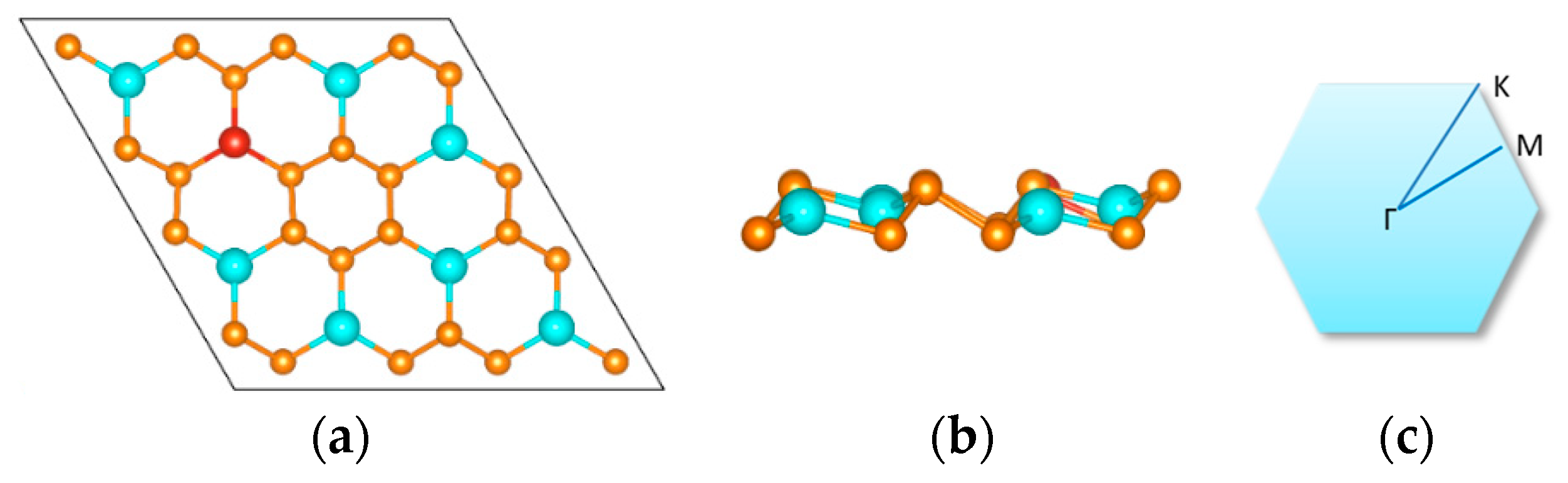
2. Materials and Methods
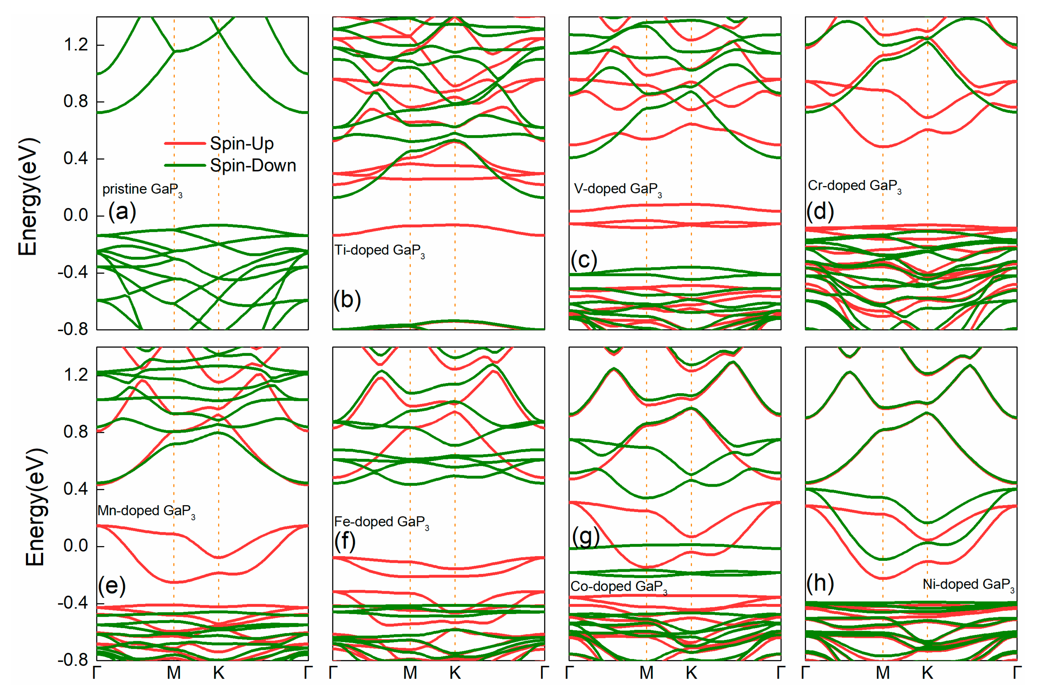
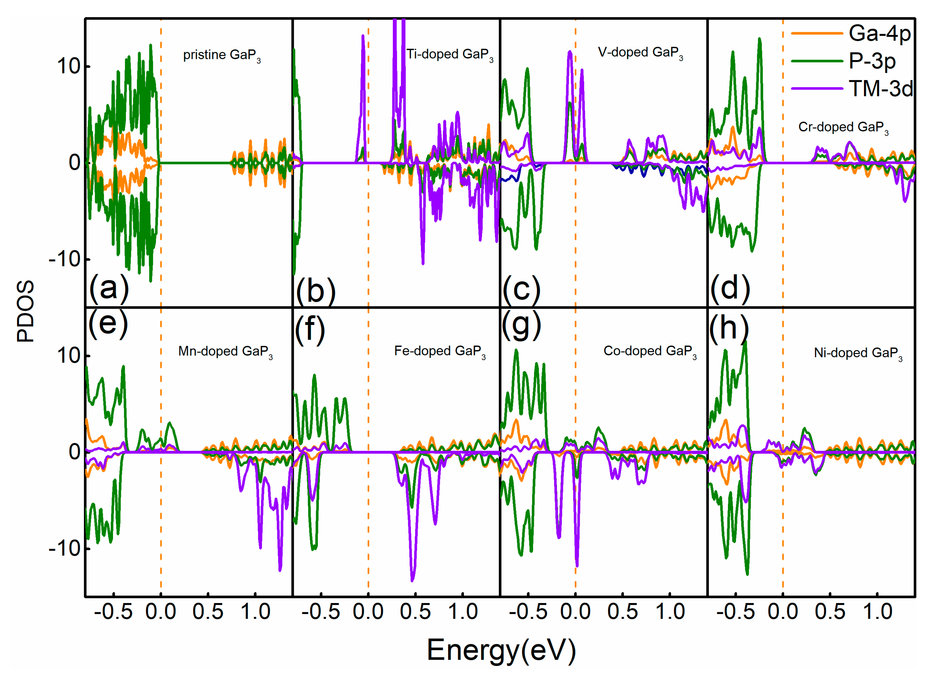
In this work, the plane wave method based on the density functional theory (DFT) was adopted for all the first-principle calculations as incorporated in the Vienna ab initio simulation package (VASP) code [46]. The projector augmented wave (PAW) method was performed for the description of electron–ion interactions of the system, and the plane wave cut-off energy was set to 500 eV [47,48]. The electron exchange-correlation function for describing the electron interactions is the generalized gradient approximation (GGA) with Pardew–Burke–Enserch (PBE) of parametrization [49]. It should be noticed that the PBE function underestimates the band gap of the system, but the tendency of band structure that adopts PBE function is unchanged. The Brillouin zone was sampled with a 5 × 5 × 1 Gamma-pack scheme grid during the structure optimization of the system. The vacuum layer of the z-direction was set to 20 Å for avoiding the influence of periodic boundary conditions. To completely relax all atoms in the supercell, the total energy and the convergence benchmark for the force were set to 10−6 eV and −0.001 eV, respectively. Firstly, the feasibility analysis of the doped system was given by calculating the bond length and the spin polarization energy. Secondly, we showed that the nonmagnetic intrinsic GaP3 obtains various magnetism after doped different 3d TM atoms. Then, we calculated and analyzed the electronic band structure in addition to the density of state (DOS) of various doped systems. Lastly, the spin density distributions for all doped systems were given.
To obtain a comprehensive understanding of monolayer GaP3, we first studied its structural properties. On the basis of our DFT calculations, as shown in Figure 1, the completely optimized doped structure is given, each dopant atom that connects to three P atoms forms three bonds, each P atom that connects one Ga atom and two P atoms forms two P–P bonds, and one Ga–P bond, respectively. There were 32 atoms in our supercell, and only one Ga atom was substituted by a 3d TM atom, so the dopant concentration was about 3.1%. The optimized lattice parameters of monolayer GaP3 are a = b = 7.21 Å, which is consistent with previous research [32].

3. Results

The bond lengths of various doped systems are shown in Table 1. It can be observed that the lengths of the P–P band and Ga–P band of the various doped system almost remain unchanged while the lengths of the dopant–P band change, but these such changes are subtle. It does not have much impact on the intrinsic structure, so these results show that the doped TM atoms can be stably embedded on the doped sites.
To gain deeper insight into the physics of these doped systems, we analyzed the spin polarization energy (Epol = Enon − Efer), as shown in Table 1, which is defined as the energy difference between the nonmagnetic state (Enon) and the ferromagnetic state (Efer). The positive value of Epol means that the energy of the ferromagnetic state is lower than the energy of the nonmagnetic state. Hence, the doped system desires to become a ferromagnetic state. Our study shows that the GaP3 systems tend to be ferromagnetic states after doping TM atoms. In addition, we also calculated the magnetic moment of different doped systems, as shown in Table 1. The magnetic moment of pure GaP3 is 0 μB, this result indicates that the intrinsic structure is nonmagnetic, and when pure GaP3 obtains doped TM atoms, it obtains different magnetic moments with different TM atoms. Moreover, we found that the magnetic moment of the Fe–doped system is 5.00 μB, which is the biggest magnetic moment of various doped systems and means that the Fe–doped system can gain the strongest ferromagnetic coupling. On the other hand, the magnetic moment of the Ni–doped system is only 0.44 μB, which means that the Ni–doped system obtains the weakest ferromagnetic coupling corresponding to the lowest Epol. Therefore, it is feasible to obtain spin polarization in monolayer GaP3 by inducing TM atoms.
Figure 2 shows the band structures of various doped systems. It is clear that monolayer GaP3 is a semiconductor with an indirect band gap of 0.79 eV at the PBE level of theory. The conduction band minimum (CBM) locates at the Γ point, while the valence band maximum (VBM) locates at the K-point, which is consistent with previous research [32]. All bands are spin degenerate after considering electronics spin; this result demonstrates that monolayer GaP3 is totally no magnetism, agreeing well with the analysis above. When doping TM atoms, as shown in Figure 2b–h, the spin degeneracy is lifted, it can be seen that the band gap values are 0.87 eV, 0.77 eV, 0.55 eV and 0.84 eV, for the Ti–, V–, Cr–and Fe–doped systems, respectively. Moreover, for the Mn–, Co– and Ni–doped systems, the impurity levels induced by Mn, Co and Ni atoms pass through the Fermi level, which means that these three systems have semi-metallic properties. The whole systems show spin polarization properties apart from the pure structure. Through the calculations and the analysis from the magnetic moments, we can initially see that the Fe–doped system obtains the strongest spin polarization property, and the Ni–doped system shows the weakest spin polarization property.
In order to investigate more about the spin polarization properties of various doped systems, we plotted the projected density of state (PDOS) near the Fermi level, as shown in Figure 3. It is clearly shown in Figure 3a that the pure GaP3 is spin energy degenerate for the spin up and spin down states, which means no spin polarization. Moreover, both the 4p orbital of the Ga atom and the 3p orbital of the P atom contributes the most to the electronic states of pure GaP3; in particular, the 4p orbital of the Ga atom plays the biggest part of it. Figure 3b–h shows the PDOS of various doped systems; we found that the spin-up and the spin-down electronic states split near the Fermi level, make the whole system asymmetric, and then the whole systems show the spin polarization properties. It is worth noting that the p–d orbital couplings between the TM atom and the GaP3 lead to the generation of the new spin states. Furthermore, the Fe– and the Ni–doped system possess the biggest and the weakest spin split, respectively, which means that the Fe–doped system has the greatest spin polarization and the Ni–doped system has the weakest spin polarization. These results correspond to the strongest and the weakest ferromagnetism, which agree well with the calculations of the magnetic moments in Table 1. Additionally, we also found an interesting result among the different doped systems. In the Fe– and Mn–doped systems, spin-up electronic states are mainly contributed by the 3p orbital of the P atom, while spin-down electronic states are mainly contributed by the 3d orbital of TM atoms near the Fermi level. However, in the Ti, V, Cr, Co and Ni–doped systems, both spin-up and spin-down electronic states are mainly contributed by the 3d orbital of TM atoms. The states near the Fermi energy are spin-nondegenerate, so the charges transferred from the TM to the GaP3 will fill these spin-polarized states, which make the TM doped GaP3 spin-polarized.
To further support the above, the charge transfers (Δq) of various doped systems were calculated by the Bader charge analysis [50], as shown in Table 1. In Table 1, the positive value means that the charge transfers from TM atoms to GaP3, vice versa. One can find that the values of Δq in the Ti–, V–, Cr–, Mn–, Fe–, Co– and Ni–doped systems are 1.22, 1.06, 0.86, 0.76, 0.60, 0.31 and 0.19 e, respectively. Different TM atoms in GaP3 show the different abilities to lose electrons. The Coulomb interaction between the different transfer charges of TM atoms and GaP3 causes the electronic structure to change differently, eventually leading to different spin polarization for various doped systems.
The spin density distributions of the various doped systems are also given in Figure 4. The spin density is defined as ∆ρs = ρ↑ − ρ↓, where ρ↑ represents the spin-up charge density, ρ↓ is the spin-down charge density. The red and blue regions in Figure 4 correspond to ∆ρs > 0 and ∆ρs < 0, respectively. It can be clearly seen that there is no spin density distribution in pure GaP3, as shown in Figure 4a, which means that the pure GaP3 has no spin polarization. However, we can find that the doped systems have spin density distributions but different from each other. Furthermore, the Fe–doped systems have the biggest area of spin density distribution, and then for the Mn–, Cr–, V–, Co–, Ti– and Ni–doped systems, the area of spin density contributions successively decrease. The whole results we obtained match well with the previous calculation of PDOS and magnetic moments. Therefore, introducing spin polarization properties by doping TM atoms is a good method for monolayer GaP3.

4. Conclusions

In our work, the electronic structure and the spin polarization properties of monolayer GaP3 induced by TM atoms (Ti, V, Cr, Mn, Fe, Co, and Ni) doping were investigated through the first-principles calculation based on density functional theory. The calculation of the bond lengths and the spin polarization energies in various doped systems were adopted to confirm the feasibility of doping TM atoms in monolayer GaP3. The various doped systems show different spin polarization properties, while the Fe–doped system can obtain the strongest magnetism than others. Based on the calculations of energy band electronic structures in TM–doped GaP3, it was found that elimination of spin degeneracy leads to asymmetry of the energy band, and then the band gaps in various doped systems changed. New spin electronic states originated from the p–d orbital couplings between TM atoms and GaP3 pass through the Fermi level, which leads to the semi-metallic property. Additionally, the spin density distributions and charge transfer for all doped systems also confirm that the TM atom doping can induce magnetism in GaP3. Our study provides a method for obtaining spin polarization in monolayer GaP3, which supports the excellent prospects for applying triphosphide in spintronic.

Author Contributions

Writing—original draft preparation, H.W.; writing—review and editing, J.G.; supervision, X.Y.; project administration, J.R. All authors have read and agreed to the published version of the manuscript.

Funding

This research was funded by the National Natural Science Foundation of China, Grant No. 11674197, and the Natural Science Foundation of Shandong Province, Grant No. ZR2018MA042.

Conflicts of Interest

The authors declare no conflict of interest.

References

  1. Novoselov, K.S.; Geim, A.K.; Morozov, S.V.; Jiang, D.; Zhang, Y.; Dubonos, S.V.; Grigorieva, I.V.; Firsov, A.A. Electric field effect in atomically thin carbon films. Science 2004, 306, 666–669. [Google Scholar] [CrossRef] [PubMed] [Green Version]
  2. AGeim, A.K.; Novoselov, K. The rise of graphene. Nat. Mater. 2007, 6, 183–191. [Google Scholar]
  3. Neto, A.H.C.; Guinea, F.; Peres, N.M.R.; Novoselov, K.S.; Geim, A.K. The electronic properties of graphene. Rev. Mod. Phys. 2009, 81, 109. [Google Scholar] [CrossRef] [Green Version]
  4. Novoselov, K.S.; Geim, A.K.; Morozov, S.V.; Jiang, D.; Katsnelson, M.I.; Grigorieva, I.V.; Dubonos, S.V.; Firsov, A.A. Two-dimensional gas of massless Dirac fermions in graphene. Nature 2005, 438, 197–200. [Google Scholar] [CrossRef] [PubMed]
  5. Stankovich, S.; Dikin, D.A.; Dommett, G.H.B.; Kohlhaas, K.M.; Zimney, E.J.; Stach, E.A.; Piner, R.D.; Nguyen, S.; Ruoff, R.S. Graphene-based composite materials. Nat. Cell Biol. 2006, 442, 282–286. [Google Scholar] [CrossRef]
  6. Zhu, H.; Zhao, L.; Liu, J.; Xu, S.; Cai, W.; Jiang, S.; Zheng, L.; Su, L.; Xu, J. Monolayer graphene saturable absorber with sandwich structure for ultrafast solid-state laser. Opt. Eng. 2015, 55, 081304. [Google Scholar] [CrossRef]
  7. Mas-Ballesté, R.; Gómez-Navarro, C.; Gomez-Herrero, J.; Zamora, F. 2D materials: To graphene and beyond. Nanoscale 2010, 3, 20–30. [Google Scholar] [CrossRef]
  8. Liu, L.; Feng, Y.P.; Shen, Z.X. Structural and electronic properties of h-BN. Phys. Rev. B 2003, 68, 104102. [Google Scholar] [CrossRef]
  9. Golberg, D.; Bando, Y.; Huang, Y.; Terao, T.; Mitome, M.; Tang, C.; Zhi, C. Boron Nitride Nanotubes and Nanosheets. ACS Nano 2010, 4, 2979–2993. [Google Scholar] [CrossRef]
  10. Warner, J.H.; Rümmeli, M.H.; Bachmatiuk, A.; Büchner, B. Atomic Resolution Imaging and Topography of Boron Nitride Sheets Produced by Chemical Exfoliation. ACS Nano 2010, 4, 1299–1304. [Google Scholar] [CrossRef]
  11. Manzeli, S.; Ovchinnikov, D.; Pasquier, D.; Yazyev, O.; Kis, A. 2D transition metal dichalcogenides. Nat. Rev. Mater. 2017, 2, 17033. [Google Scholar] [CrossRef]
  12. Wang, Q.-H.; Zadeh, K.K.; Kis, A.; Coleman, J.N.; Strano, M.S. Electronics and optoelectronics of two-dimensional transition metal dichalcogenides. Nat. Nanotechol. 2012, 7, 699–712. [Google Scholar] [CrossRef] [PubMed]
  13. Jariwala, D.; Sangwan, V.K.; Lauhon, L.; Marks, T.J.; Hersam, M.C. Emerging Device Applications for Semiconducting Two-Dimensional Transition Metal Dichalcogenides. ACS Nano 2014, 8, 1102–1120. [Google Scholar] [CrossRef] [PubMed] [Green Version]
  14. Xu, X.; Yao, W.; Xiao, D.; Heinz, T.F. Spin and pseudospins in layered transition metal dichalcogenides. Nat. Phys. 2014, 10, 343–350. [Google Scholar] [CrossRef]
  15. Qian, X.; Liu, J.; Fu, L.; Liu, J. Quantum spin Hall effect in two-dimensional transition metal dichalcogenides. Science 2014, 346, 1344–1347. [Google Scholar] [CrossRef] [Green Version]
  16. Kou, L.; Chen, C.; Smith, S.C. Phosphorene: Fabrication, Properties, and Applications. J. Phys. Chem. Lett. 2015, 6, 2794–2805. [Google Scholar] [CrossRef] [Green Version]
  17. Carvalho, A.; Wang, M.; Zhu, X.; Rodin, A.S.; Su, H.; Neto, A.H.C. Phosphorene: From theory to applications. Nat. Rev. Mater. 2016, 1, 16061. [Google Scholar] [CrossRef]
  18. Liu, H.; Neal, A.; Zhu, Z.; Luo, Z.; Xu, X.; Tománek, D.; Ye, P.D. Phosphorene: An Unexplored 2D Semiconductor with a High Hole Mobility. ACS Nano 2014, 8, 4033–4041. [Google Scholar] [CrossRef] [Green Version]
  19. Xiao, P.; Sk, M.A.; Thia, L.; Ge, X.; Lim, R.J.; Wang, J.-Y.; Lim, K.H.; Wang, X. Molybdenum phosphide as an efficient electrocatalyst for the hydrogen evolution reaction. Energy Environ. Sci. 2014, 7, 2624–2629. [Google Scholar] [CrossRef] [Green Version]
  20. Popczun, E.J.; McKone, J.R.; Read, C.G.; Biacchi, A.J.; Wiltrout, A.M.; Lewis, N.S.; Schaak, R.E. Nanostructured Nickel Phosphide as an Electrocatalyst for the Hydrogen Evolution Reaction. J. Am. Chem. Soc. 2013, 135, 9267–9270. [Google Scholar] [CrossRef]
  21. Shahzad, F.; Alhabeb, M.; Hatter, C.B.; Anasori, B.; Hong, S.M.; Koo, C.M.; Gogotsi, Y. Electromagnetic interference shielding with 2D transition metal carbides (MXenes). Science 2016, 353, 1137–1140. [Google Scholar] [CrossRef] [PubMed] [Green Version]
  22. Naguib, M.; Mochalin, V.; Barsoum, M.W.; Gogotsi, Y. 25th Anniversary Article: MXenes: A New Family of Two-Dimensional Materials. Adv. Mater. 2014, 26, 992–1005. [Google Scholar] [CrossRef] [PubMed]
  23. Anasori, B.; Lukatskaya, M.R.; Gogotsi, Y. 2D metal carbides and nitrides (MXenes) for energy storage. Nat. Rev. Mater. 2017, 2, 16098. [Google Scholar] [CrossRef]
  24. Sun, S.; Meng, F.; Wang, H.; Wang, H.; Ni, Y. Novel two-dimensional semiconductor SnP3: High stability, tunable bandgaps and high carrier mobility explored using first-principles calculations. J. Mater. Chem. A 2018, 6, 11890–11897. [Google Scholar] [CrossRef]
  25. Slassi, A.; Gali, S.M.; Pershin, A.; Gali, A.; Cornil, J.; Beljonne, D. Interlayer Bonding in Two-Dimensional Materials: The Special Case of SnP3 and GeP3. J. Phys. Chem. Lett. 2020, 11, 4503–4510. [Google Scholar] [CrossRef]
  26. Miao, N.; Xu, B.; Bristowe, N.C.; Zhou, J.; Sun, Z. Tunable Magnetism and Extraordinary Sunlight Absorbance in Indium Triphosphide Monolayer. J. Am. Chem. Soc. 2017, 139, 11125–11131. [Google Scholar] [CrossRef] [Green Version]
  27. Ghosh, B.; Puri, S.; Agarwal, A.; Bhowmick, S. SnP3: A Previously Unexplored Two-Dimensional Material. J. Phys. Chem. C 2018, 122, 18185–18191. [Google Scholar] [CrossRef]
  28. Shojaei, F.; Kang, H.S. Partially planar BP3 with high electron mobility as a phosphorene analog. J. Mater. Chem. C 2017, 5, 11267–11274. [Google Scholar] [CrossRef]
  29. Lu, N.; Zhuo, Z.; Guo, H.; Wu, P.; Fa, W.; Wu, X.; Zeng, X.-C. CaP3: A New Two-Dimensional Functional Material with Desirable Bandgap and Ultrahigh Carrier Mobility. J. Phys. Chem. Lett. 2018, 9, 1728–1733. [Google Scholar] [CrossRef] [Green Version]
  30. Jing, Y.; Ma, Y.; Li, Y.; Heine, T. GeP3: A Small Indirect Band Gap 2D Crystal with High Carrier Mobility and Strong Interlayer Quantum Confinement. Nano Lett. 2017, 17, 1833–1838. [Google Scholar] [CrossRef] [Green Version]
  31. Liu, H.-Y.; Yang, C.-L.; Wang, M.-S.; Ma, X.-G. Two-dimensional BiP3 with high carrier mobility and moderate band gap for hydrogen generation from water splitting. Appl. Surf. Sci. 2020, 501, 144263. [Google Scholar] [CrossRef]
  32. Yao, S.; Zhang, X.; Zhang, Z.; Chen, A.; Zhou, Z. 2D Triphosphides: SbP3 and GaP3 monolayer as promising photocatalysts for water splitting. Int. J. Hydrogen Energy 2019, 44, 5948–5954. [Google Scholar] [CrossRef]
  33. Sun, Z.; Yuan, K.; Chang, Z.; Bi, S.; Zhang, X.; Tang, D. Ultra-low thermal conductivity and high thermoelectric performance of two-dimensional triphosphides (InP3, GaP3, SbP3 and SnP3): A comprehensive first-principles study. Nanoscale 2020, 12, 3330–3342. [Google Scholar] [CrossRef] [PubMed]
  34. Zhang, Z.; Zou, X.; Crespi, V.H.; Yakobson, B.I. Intrinsic Magnetism of Grain Boundaries in Two-Dimensional Metal Dichalcogenides. ACS Nano 2013, 7, 10475–10481. [Google Scholar] [CrossRef] [Green Version]
  35. Guan, J.; Yu, G.; Ding, X.; Chen, W.; Shi, Z.; Huang, X.; Sun, C. The Effects of the Formation of Stone–Wales Defects on the Electronic and Magnetic Properties of Silicon Carbide Nanoribbons: A First-Principles Investigation. Chem. Phys. Chem. 2013, 14, 2841–2852. [Google Scholar] [CrossRef] [PubMed]
  36. Gao, G.; Ding, G.; Li, J.; Yao, K.; Wu, M.; Guangqian, D. Monolayer MXenes: Promising half-metals and spin gapless semiconductors. Nanoscale 2016, 8, 8986–8994. [Google Scholar] [CrossRef] [PubMed] [Green Version]
  37. Yang, Y.; Guo, M.; Zhang, G.; Li, W. Tuning the electronic and magnetic properties of porous graphene-like carbon nitride through 3d transition-metal doping. Carbon 2017, 117, 120–125. [Google Scholar] [CrossRef]
  38. Zhao, X.; Qiu, B.; Hu, G.; Yue, W.; Ren, J.; Yuan, X. Spin Polarization Properties of Pentagonal PdSe2 Induced by 3D Transition-Metal Doping: First-Principles Calculations. Materials 2018, 11, 2339. [Google Scholar] [CrossRef] [Green Version]
  39. Li, Y.; Qiu, B.; Zhao, X.; Hu, G.; Yue, W.; Yuan, X.; Ren, J. Spin polarization properties of two-dimensional MoSeTe induced by transition-metal doping: First-principles calculations. Eur. Phys. J. B 2019, 92, 266. [Google Scholar] [CrossRef]
  40. Chen, Q.; Ouyang, Y.; Yuan, S.; Li, R.; Wang, J. Uniformly Wetting Deposition of Co Atoms on MoS2 Monolayer: A Promising Two-Dimensional Robust Half-Metallic Ferromagnet. ACS Appl. Mater. Interfaces 2014, 6, 16835–16840. [Google Scholar] [CrossRef]
  41. Kan, E.J.; Xiang, H.; Wu, F.; Tian, C.; Lee, C.; Yang, J.L.; Whangbo, M.-H. Prediction for room-temperature half-metallic ferromagnetism in the half-fluorinated single layers of BN and ZnO. Appl. Phys. Lett. 2010, 97, 122503. [Google Scholar] [CrossRef]
  42. Yuan, X.; Yang, M.; Tian, Y.; Cai, L.; Ren, J. Spin polarization properties of thiophene molecule adsorbed to the edge of zigzag graphene nanoribbon. Synth. Met. 2017, 226, 46–49. [Google Scholar] [CrossRef]
  43. Yuan, X.; Tian, Y.; Zhao, X.; Yue, W.; Hu, G.; Ren, J. Spin polarization properties of benzene/graphene with transition metals as dopants: First principles calculations. Appl. Surf. Sci. 2018, 439, 1158–1162. [Google Scholar] [CrossRef]
  44. Hashmi, A.; Hong, J. Transition Metal Doped Phosphorene: First-Principles Study. J. Phys. Chem. C 2015, 119, 9198–9204. [Google Scholar] [CrossRef]
  45. Barone, V.; Peralta, J. Magnetic Boron Nitride Nanoribbons with Tunable Electronic Properties. Nano Lett. 2008, 8, 2210–2214. [Google Scholar] [CrossRef] [Green Version]
  46. Kresse, G.; Furthmüller, J. Efficient iterative schemes for ab initio total-energy calculations using a plane-wave basis set. Phys. Rev. B 1996, 54, 11169. [Google Scholar] [CrossRef]
  47. Blöchl, P.E. Projector augmented-wave method. Phys. Rev. B 1994, 50, 17953. [Google Scholar] [CrossRef] [Green Version]
  48. Kresse, G.; Joubert, D. From ultrasoft pseudopotentials to the projector augmented-wave method. Phys. Rev. B 1999, 59, 1758. [Google Scholar] [CrossRef]
  49. Perdew, J.P.; Burke, K.; Ernzerhof, M. Generalized Gradient Approximation Made Simple. Phys. Rev. Lett. 1996, 77, 3865. [Google Scholar] [CrossRef] [Green Version]
  50. Tang, W.; Sanville, E.; Henkelman, G. A grid-based Bader analysis algorithm without lattice bias. J. Phys. Condens. Matter 2009, 21, 084204. [Google Scholar] [CrossRef]
Figure 1. Top (a) and side (b) views of monolayer GaP3 structure. The blue, orange and red balls represent Ga, P and TM dopant (Ti, V, Cr, Mn, Fe, Co, Ni), respectively. The first Brillouin zone with high symmetry k points (Γ, M and K) is shown in (c).
Micromachines 12 00743 g001
Figure 2. The electronic band structures of different doped GaP3 systems, (a) pure GaP3, (b) Ti–doped GaP3, (c) V–doped GaP3, (d) Cr–doped GaP3, (e) Mn–doped GaP3, (f) Fe–doped GaP3, (g) Co–doped GaP3 and (h) Ni–doped GaP3, respectively.
Micromachines 12 00743 g002
Figure 3. Projected density of states (PDOS) of the different doped systems, (a) pure system, (b) Ti–doped system, (c) V–doped system, (d) Cr–doped system, (e) Mn–doped system, (f) Fe–doped system, (g) Co–doped system and (h) Ni–doped system, respectively.
Micromachines 12 00743 g003
Figure 4. Spin density distributions for different doped systems. (ah) correspond to pure GaP3, Ti–, V–, Cr–, Mn–, Fe–, Co– and Ni–doped, respectively. The 2D planes are determined by three Ga atoms and the dopants for the doped system, three P atoms for pure GaP3.
Micromachines 12 00743 g004
Table 1. The bond length, spin polarization energy, charge transfer, and magnetic moment of various doped systems.
SystemTi-DopedV-DopedCr-DopedMn-DopedFe-DopedCo-DopedNi-DopedPure
Bond length (Å)P-P2.232.242.252.222.212.252.252.23
Ga-P2.362.352.352.372.362.342.352.36
TM-P2.422.372.382.322.232.232.24-
Epol (eV)3.734.164.954.833.882.261.18-
Δq (e)1.221.060.860.760.600.310.19-
Magnetic moment (μB)1.002.003.004.005.001.440.440.00
Publisher’s Note: MDPI stays neutral with regard to jurisdictional claims in published maps and institutional affiliations.

