
Bulk versus Contact Doping in Organic Semiconductors


Abstract
:1. Introduction
2. Experimental and Simulation Methods
3. Results and Discussion
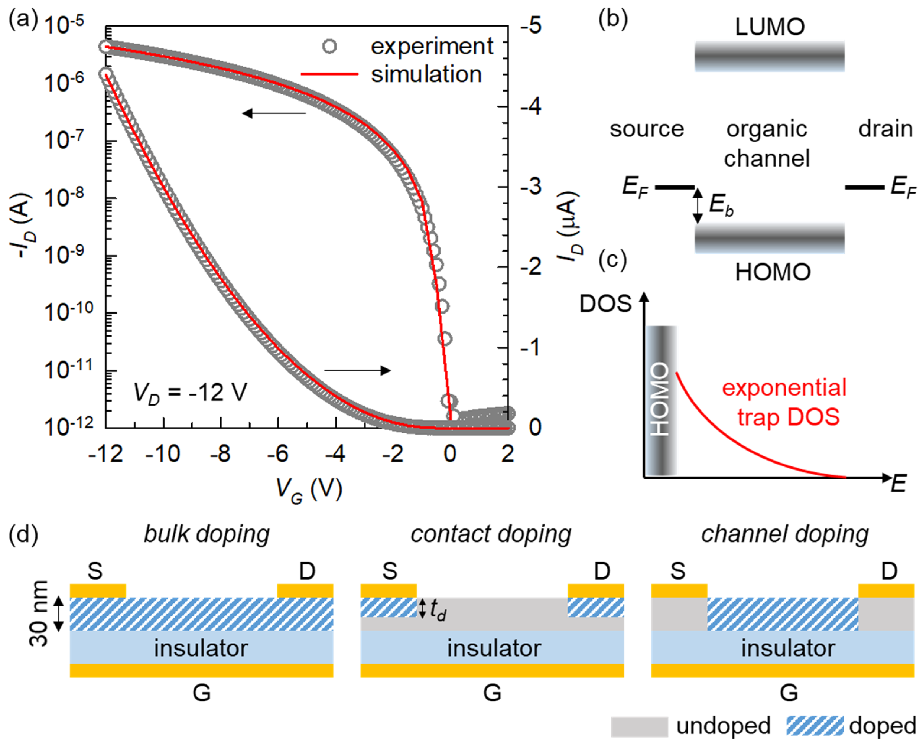
3.1. Validity of Simulation Framework
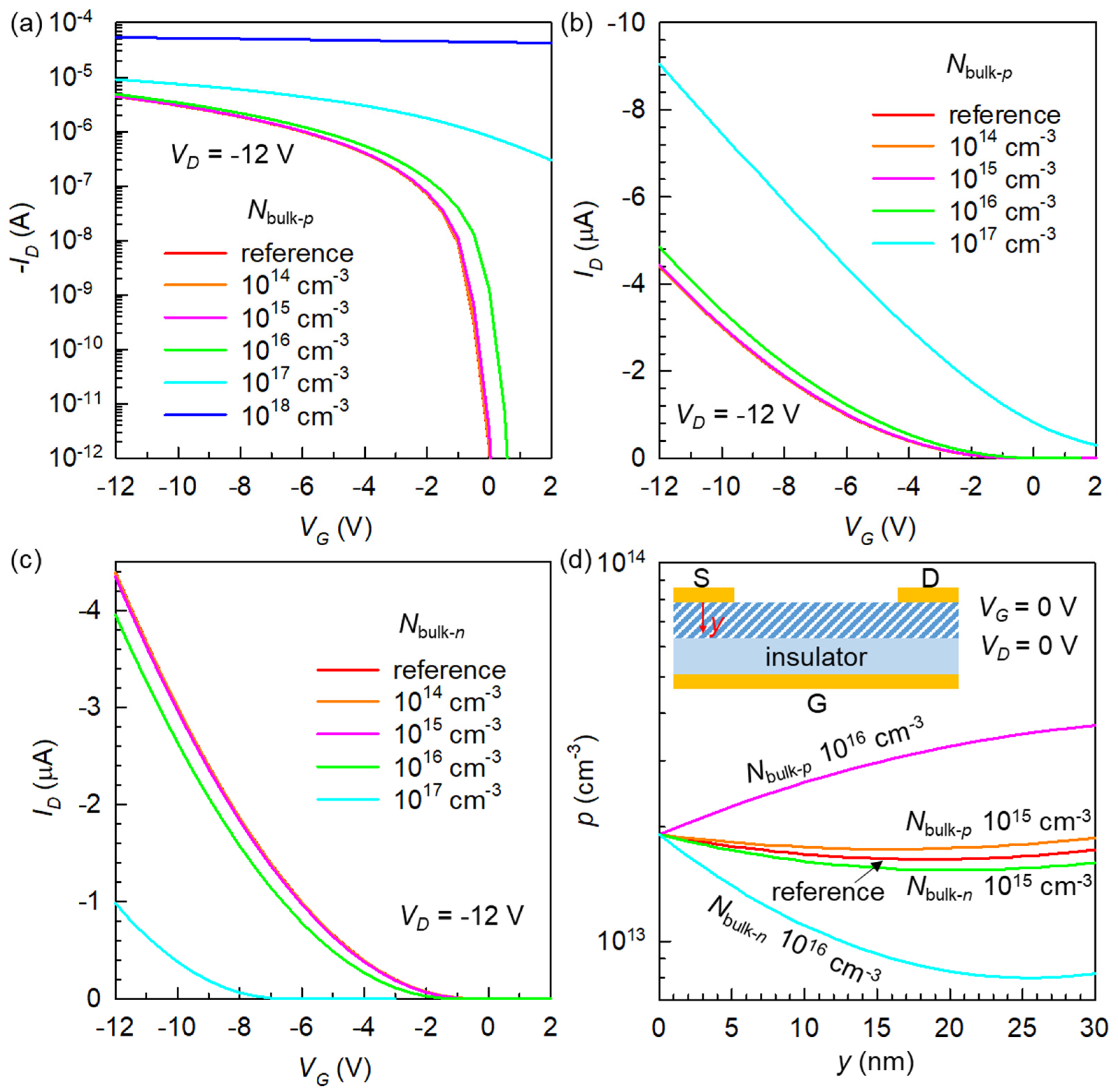
3.2. Bulk Doping
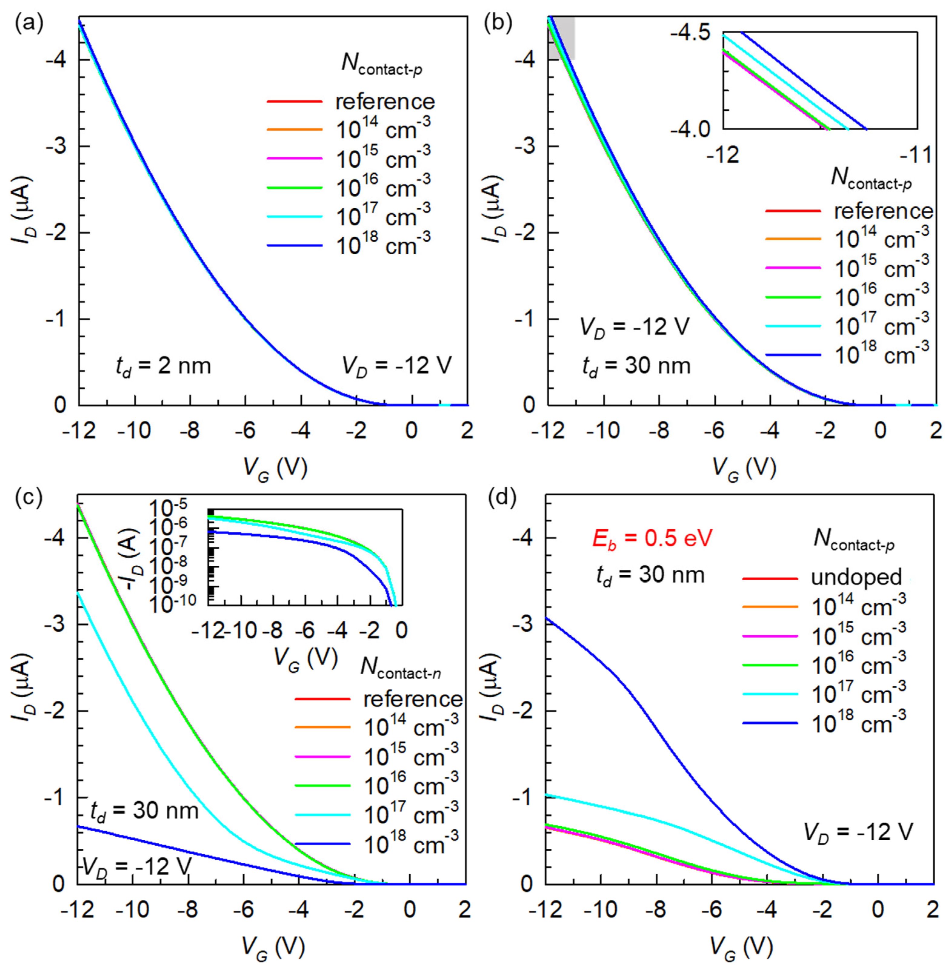
3.3. Contact Doping
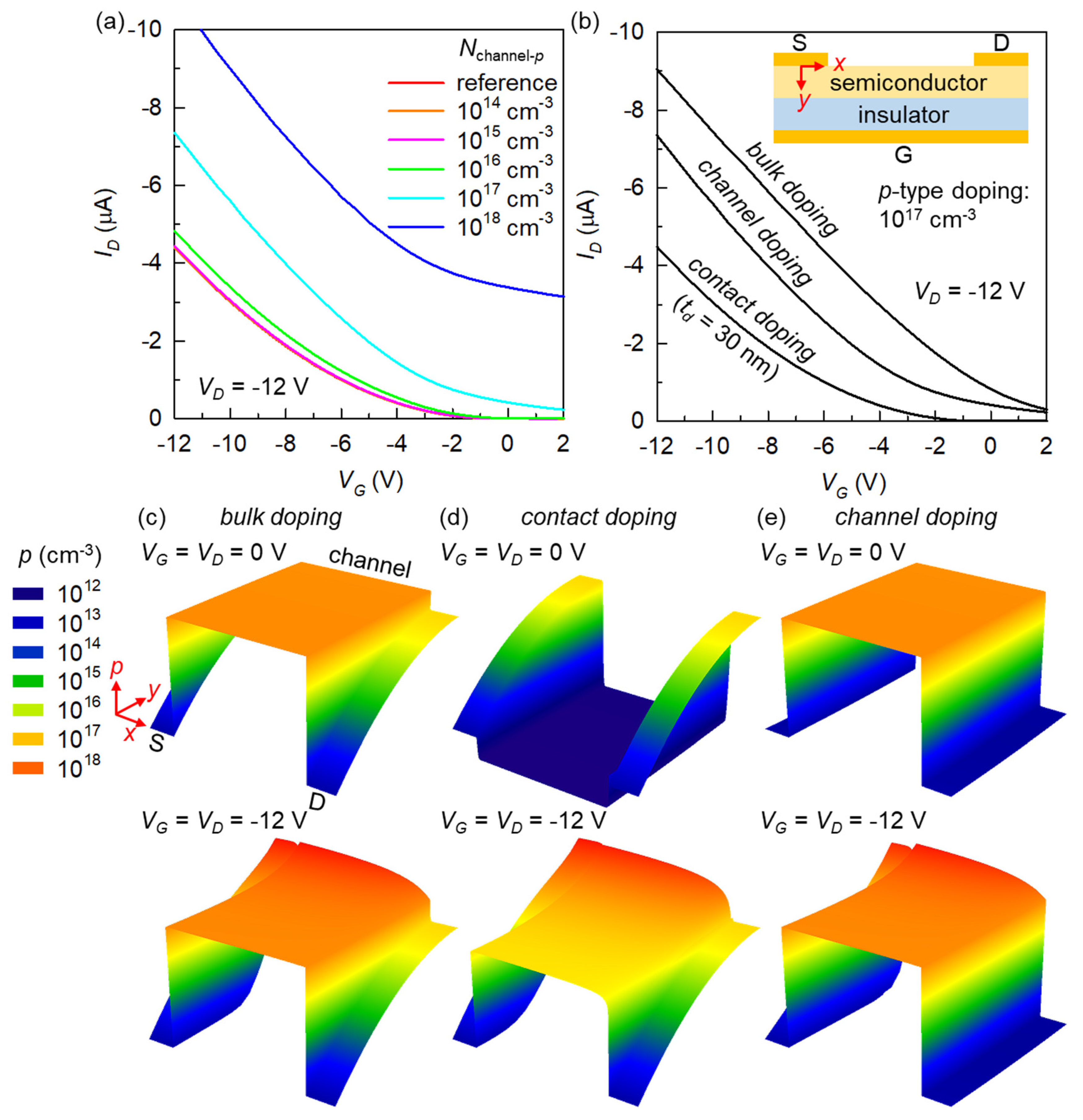
3.4. Comparative Analysis
4. Conclusions
Funding
Conflicts of Interest
References
- Facchetti, A. Semiconductors for Organic Transistors. Mater. Today 2007, 10, 28–37. [Google Scholar] [CrossRef]
- Anthony, J.E.; Facchetti, A.; Heeney, M.; Marder, S.R.; Zhan, X. n-Type Organic Semiconductors in Organic Electronics. Adv. Mater. 2010, 22, 3876–3892. [Google Scholar] [CrossRef]
- Takimiya, K.; Shinamura, S.; Osaka, I.; Miyazaki, E. Thienoacene-Based Organic Semiconductors. Adv. Mater. 2011, 23, 4347–4370. [Google Scholar] [CrossRef]
- Geffroy, B.; le Roy, P.; Prat, C. Organic Light-Emitting Diode (OLED) Technology: Materials, Devices and Display Technologies. Polym. Int. 2006, 55, 572–582. [Google Scholar] [CrossRef]
- Kippelen, B.; Bredas, J.-L. Organic Photovoltaics. Energy Environ. Sci. 2009, 2, 251–261. [Google Scholar] [CrossRef]
- Lamport, Z.A.; Haneef, H.F.; Anand, S.; Waldrip, M.; Jurchescu, O.D. Tutorial: Organic Field-Effect Transistors: Materials, Structure and Operation. J. Appl. Phys. 2018, 124, 071101. [Google Scholar] [CrossRef]
- Sirringhaus, H. Organic Field-Effect Transistors: The Path Beyond Amorphous Silicon. Adv. Mater. 2014, 26, 1319–1335. [Google Scholar] [CrossRef] [Green Version]
- Paterson, A.F.; Singh, S.; Fallon, K.J.; Hodsden, T.; Han, Y.; Schroeder, B.; Bronstein, H.; Heeney, M.; McCulloch, I.; Anthopoulos, T.D. Recent Progress in High-Mobility Organic Transistors: A Reality Check. Adv. Mater. 2018, 30, 1801079. [Google Scholar] [CrossRef] [PubMed]
- Zschieschang, U.; Borchert, J.W.; Giorgio, M.; Caironi, M.; Letzkus, F.; Burghartz, J.N.; Waizmann, U.; Weis, J.; Ludwigs, S.; Klauk, H. Roadmap to Gigahertz Organic Transistors. Adv. Funct. Mater. 2020, 30, 1903812. [Google Scholar] [CrossRef] [Green Version]
- Jung, S.; Bonnassieux, Y.; Horowitz, G.; Jung, S.; Iñiguez, B.; Kim, C.-H. Advances in Compact Modeling of Organic Field-Effect Transistors. IEEE J. Electron Devices Soc. 2020, 8, 1404–1415. [Google Scholar] [CrossRef]
- Xiaochen, R.; Fangxu, Y.; Xiong, G.; Shanshan, C.; Xiaotao, Z.; Huanli, D.; Wenping, H. Organic Field-Effect Transistor for Energy-Related Applications: Low-Power-Consumption Devices, Near-Infrared Phototransistors, and Organic Thermoelectric Devices. Adv. Energy Mater. 2018, 8, 1801003. [Google Scholar]
- van de Burgt, Y.; Melianas, A.; Keene, S.T.; Malliaras, G.; Salleo, A. Organic Electronics for Neuromorphic Computing. Nat. Electron. 2018, 1, 386–397. [Google Scholar] [CrossRef]
- Yuvaraja, S.; Nawaz, A.; Liu, Q.; Dubal, D.; Surya, S.G.; Salama, K.N.; Sonar, P. Organic Field-Effect Transistor-Based Flexible Sensors. Chem. Soc. Rev. 2020, 49, 3423–3460. [Google Scholar] [CrossRef] [PubMed]
- Olthof, S.; Mehraeen, S.; Mohapatra, S.K.; Barlow, S.; Coropceanu, V.; Brédas, J.-L.; Marder, S.R.; Kahn, A. Ultralow Doping in Organic Semiconductors: Evidence of Trap Filling. Phys. Rev. Lett. 2012, 109, 176601. [Google Scholar] [CrossRef]
- Xu, Y.; Sun, H.; Liu, A.; Zhu, H.-H.; Li, W.; Lin, Y.-F.; Noh, Y.-Y. Doping: A Key Enabler for Organic Transistors. Adv. Mater. 2018, 30, 1801830. [Google Scholar] [CrossRef]
- Tang, C.G.; Ang, M.C.Y.; Choo, K.-K.; Keerthi, V.; Tan, J.-K.; Syafiqah, M.N.; Kugler, T.; Burroughes, J.H.; Png, R.-Q.; Chua, L.-L.; et al. Doped Polymer Semiconductors with Ultrahigh and Ultralow Work Functions for Ohmic Contacts. Nature 2016, 539, 536–540. [Google Scholar] [CrossRef]
- Kim, C.H.; Yaghmazadeh, O.; Tondelier, D.; Jeong, Y.B.; Bonnassieux, Y.; Horowitz, G. Capacitive Behavior of Pentacene-Based Diodes: Quasistatic Dielectric Constant and Dielectric Strength. J. Appl. Phys. 2011, 109, 083710. [Google Scholar] [CrossRef] [Green Version]
- Kim, C.H.; Bonnassieux, Y.; Horowitz, G. Charge Distribution and Contact Resistance Model for Coplanar Organic Field-Effect Transistors. IEEE Trans. Electron Devices 2013, 60, 280–287. [Google Scholar] [CrossRef] [Green Version]
- Kim, C.-H.; Thomas, S.; Kim, J.H.; Elliott, M.; Macdonald, J.E.; Yoon, M.-H. Potentiometric Parameterization of Dinaphtho[2,3-b:2’,3’-f]thieno[3,2-b]thiophene Field-Effect Transistors with a Varying Degree of Nonidealities. Adv. Electron. Mater. 2018, 4, 1700514. [Google Scholar] [CrossRef]
- Kim, C.-H. Self-Rectifying DNTT Memristors. IEEE Electron Device Lett. 2018, 39, 1736–1739. [Google Scholar] [CrossRef]
- Kim, C.-H. Improved Device Ideality in Aged Organic Transistors. Electron. Mater. Lett. 2019, 15, 166–170. [Google Scholar] [CrossRef]
- Kim, C.H.; Bonnassieux, Y.; Horowitz, G. Fundamental Benefits of the Staggered Geometry for Organic Field-Effect Transistors. IEEE Electron Device Lett. 2011, 32, 1302–1304. [Google Scholar] [CrossRef] [Green Version]
- Kim, C.-H.; Choi, J.; Bonnassieux, Y.; Horowitz, G. Simplified Numerical Simulation of Organic Photovoltaic Devices. J. Comput. Electron. 2016, 15, 1095–1102. [Google Scholar] [CrossRef]
- Han, H.; Kim, C.-H. Unexpected Benefits of Contact Resistance in 3D Organic Complementary Inverters. Adv. Electron. Mater. 2020, 6, 1900879. [Google Scholar] [CrossRef]
- Kim, C.-H.; Hayakawa, R.; Wakayama, Y. Fundamentals of Organic Anti-Ambipolar Ternary Inverters. Adv. Electron. Mater. 2020, 6, 1901200. [Google Scholar] [CrossRef]
- Sporea, R.A.; Trainor, M.J.; Young, N.D.; Shannon, J.M.; Silva, S.R.P. Source-Gated Transistors for Order-of-Magnitude Performance Improvements in Thin-Film Digital Circuits. Sci. Rep. 2014, 4, 4295. [Google Scholar] [CrossRef] [PubMed] [Green Version]
- Drury, R.; Bestelink, E.; Sporea, R.A. Simulation Study of Overlap Capacitance in Source-Gated Transistors for Current-Mode Pixel Drivers. IEEE Electron Device Lett. 2019, 40, 1451–1454. [Google Scholar] [CrossRef] [Green Version]
- Jung, S.; Jin, J.W.; Mosser, V.; Bonnassieux, Y.; Horowitz, G. A Compact Model and Parameter Extraction Method for a Staggered OFET with Power-Law Contact Resistance and Mobility. IEEE Trans. Electron Devices 2019, 66, 4894–4900. [Google Scholar] [CrossRef]
- Lee, Y.; Horowitz, G.; Jung, S.; Bonnassieux, Y. Validity of the Effective Injection Barrier in Organic Field-Effect Transistors. J. Phys. D Appl. Phys. 2020, 54, 095109. [Google Scholar] [CrossRef]
- Natali, D.; Caironi, M. Charge Injection in Solution-Processed Organic Field-Effect Transistors: Physics, Models and Characterization Methods. Adv. Mater. 2012, 24, 1357–1387. [Google Scholar] [CrossRef] [PubMed]
- Waldrip, M.; Jurchescu, O.D.; Gundlach, D.J.; Bittle, E.G. Contact Resistance in Organic Field-Effect Transistors: Conquering the Barrier. Adv. Funct. Mater. 2019, 30, 1904576. [Google Scholar] [CrossRef]
- Kim, C.-H. Contact Resistance in Organic Transistors: Use It or Remove It. Appl. Phys. Rev. 2020, 7, 031306. [Google Scholar] [CrossRef]
- Kalb, W.L.; Batlogg, B. Calculating the Trap Density of States in Organic Field-Effect Transistors from Experiment: A Comparison of Different Methods. Phys. Rev. B 2010, 81, 035327. [Google Scholar] [CrossRef] [Green Version]
- Kim, C.H.; Castro-Carranza, A.; Estrada, M.; Cerdeira, A.; Bonnassieux, Y.; Horowitz, G.; Iñiguez, B. A Compact Model for Organic Field-Effect Transistors with Improved Output Asymptotic Behaviors. IEEE Trans. Electron Devices 2013, 60, 1136–1141. [Google Scholar]
- Venkateshvaran, D.; Nikolka, M.; Sadhanala, A.; Lemaur, V.; Zelazny, M.; Kepa, M.; Hurhangee, M.; Kronemeijer, A.J.; Pecunia, V.; Nasrallah, I.; et al. Approaching Disorder-Free Transport in High-Mobility Conjugated Polymers. Nature 2014, 515, 384–388. [Google Scholar] [CrossRef] [PubMed] [Green Version]
- Belasco, J.; Mohapatra, S.K.; Zhang, Y.; Barlow, S.; Marder, S.R.; Kahn, A. Molecular Doping and Tuning Threshold Voltage in 6,13-Bis(triisopropylsilylethynyl)pentacene/Polymer Blend Transistors. Appl. Phys. Lett. 2014, 105, 063301. [Google Scholar] [CrossRef]
- Yurash, B.; Cao, D.X.; Brus, V.V.; Leifert, D.; Wang, M.; Dixon, A.; Seifrid, M.; Mansour, A.E.; Lungwitz, D.; Liu, T.; et al. Towards Understanding the Doping Mechanism of Organic Semiconductors by Lewis Acids. Nat. Mater. 2019, 18, 1327–1334. [Google Scholar] [CrossRef]
- Peterson, K.A.; Patterson, A.; Vega-Flick, A.; Liao, B.; Chabinyc, M.L. Doping Molecular Organic Semiconductors by Diffusion from the Vapor Phase. Mater. Chem. Front. 2020, 4, 3632–3639. [Google Scholar] [CrossRef]
- Ante, F.; Kälblein, D.; Zschieschang, U.; Canzler, T.W.; Werner, A.; Takimiya, K.; Ikeda, M.; Sekitani, T.; Someya, T.; Klauk, H. Contact Doping and Ultrathin Gate Dielectrics for Nanoscale Organic Thin-Film Transistors. Small 2011, 7, 1186–1191. [Google Scholar] [CrossRef] [PubMed]
- Kim, Y.; Chung, S.; Cho, K.; Harkin, D.; Hwang, W.-T.; Yoo, D.; Kim, J.-K.; Lee, W.; Song, Y.; Ahn, H.; et al. Enhanced Charge Injection Properties of Organic Field-Effect Transistor by Molecular Implantation Doping. Adv. Mater. 2019, 31, 1806697. [Google Scholar] [CrossRef] [PubMed]
- Singh, S.; Mohapatra, S.K.; Sharma, A.; Fuentes-Hernandez, C.; Barlow, S.; Marder, S.R.; Kippelen, B. Reduction of Contact Resistance by Selective Contact Doping in Fullerene n-Channel Organic Field-Effect Transistors. Appl. Phys. Lett. 2013, 102, 153303. [Google Scholar] [CrossRef]
- Hou, J.-L.; Kasemann, D.; Widmer, J.; Günther, A.A.; Lüssem, B.; Leo, K. Reduced Contact Resistance in Top-Contact Organic Field-Effect Transistors by Interface Contact Doping. Appl. Phys. Lett. 2016, 108, 103303. [Google Scholar] [CrossRef]
- Pei, K.; Lau, A.H.Y.; Chan, P.K.L. Understanding Molecular Surface Doping of Large Bandgap Organic Semiconductors and Overcoming the Contact/Access Resistance in Organic Field-Effect Transistors. Phys. Chem. Chem. Phys. 2020, 22, 7100–7109. [Google Scholar] [CrossRef]
- Khim, D.; Baeg, K.-J.; Caironi, M.; Liu, C.; Xu, Y.; Kim, D.-Y.; Noh, Y.-Y. Control of Ambipolar and Unipolar Transport in Organic Transistors by Selective Inkjet-Printed Chemical Doping for High Performance Complementary Circuits. Adv. Funct. Mater. 2014, 24, 6252–6261. [Google Scholar] [CrossRef]
- Horowitz, G. Organic Thin Film Transistors: From Theory to Real Devices. J. Mater. Res. 2004, 19, 1946–1962. [Google Scholar] [CrossRef] [Green Version]
- Kim, C.-H.; Kymissis, I. Graphene–Organic Hybrid Electronics. J. Mater. Chem. C 2017, 5, 4598–4613. [Google Scholar] [CrossRef]


| Layer | Parameter | Value |
|---|---|---|
| Organic semiconductor | Electron affinity | 2.0 eV |
| Band gap | 3.3 eV | |
| Doping concentration | 0 cm−3 | |
| Hole mobility | 1 cm2V−1s−1 | |
| HOMO effective DOS | 1020 cm−3 | |
| Total trap density | 1017 cm−3 | |
| Trap characteristic temperature | 1200 K | |
| Gate electrode | Work function | 5.0 eV |
| Source/drain electrodes | Work function | 4.9 eV |
Publisher’s Note: MDPI stays neutral with regard to jurisdictional claims in published maps and institutional affiliations. |
© 2021 by the author. Licensee MDPI, Basel, Switzerland. This article is an open access article distributed under the terms and conditions of the Creative Commons Attribution (CC BY) license (https://creativecommons.org/licenses/by/4.0/).
Share and Cite
Kim, C.-H. Bulk versus Contact Doping in Organic Semiconductors. Micromachines 2021, 12, 742. https://doi.org/10.3390/mi12070742
Kim C-H. Bulk versus Contact Doping in Organic Semiconductors. Micromachines. 2021; 12(7):742. https://doi.org/10.3390/mi12070742
Chicago/Turabian StyleKim, Chang-Hyun. 2021. "Bulk versus Contact Doping in Organic Semiconductors" Micromachines 12, no. 7: 742. https://doi.org/10.3390/mi12070742
APA StyleKim, C.-H. (2021). Bulk versus Contact Doping in Organic Semiconductors. Micromachines, 12(7), 742. https://doi.org/10.3390/mi12070742