
Random Telegraph Noise in 3D NAND Flash Memories


Abstract
1. Introduction
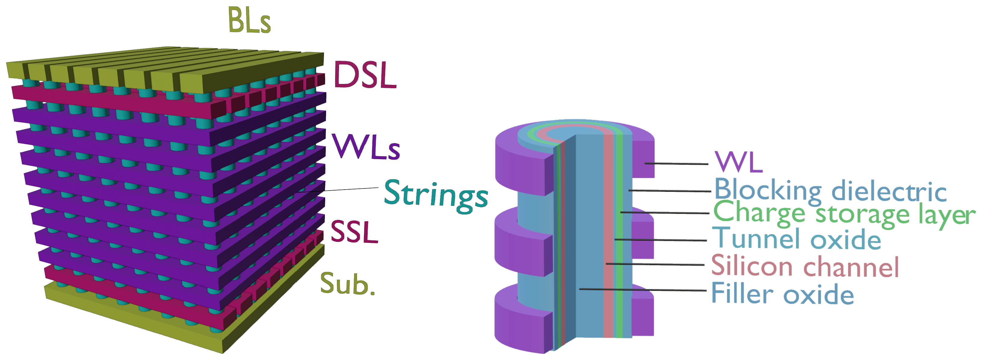
2. Array and Cell Structure
3. Polysilicon Conduction
4. Experimental Data
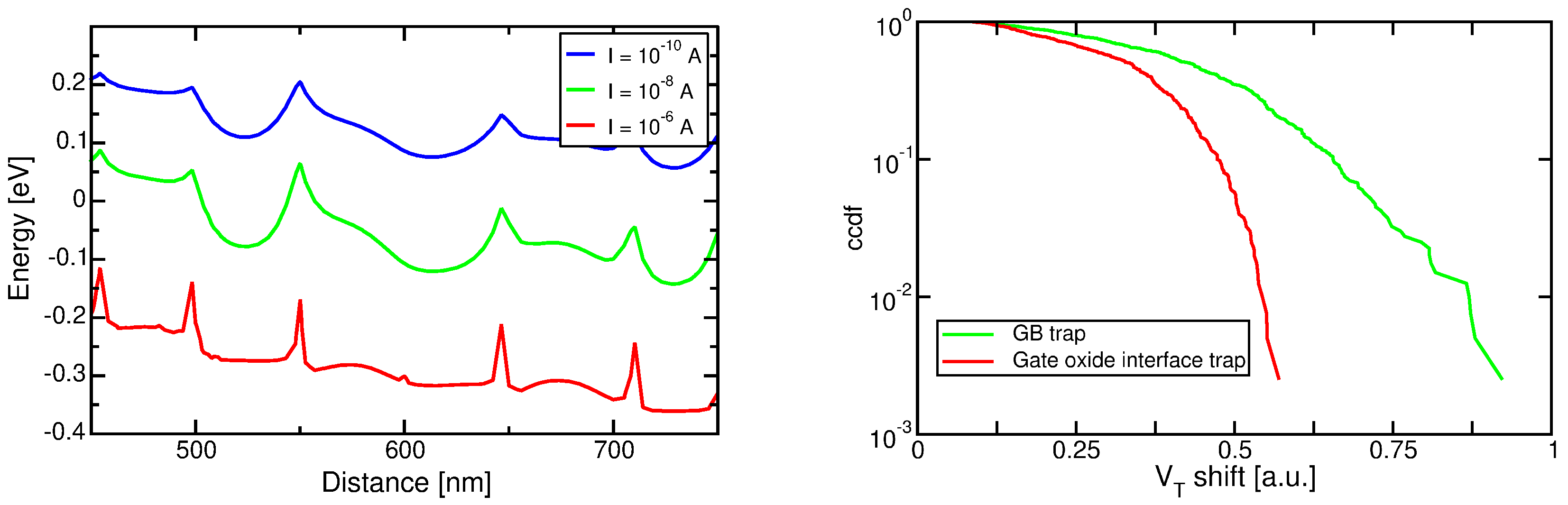
4.1. Single-Trap Data
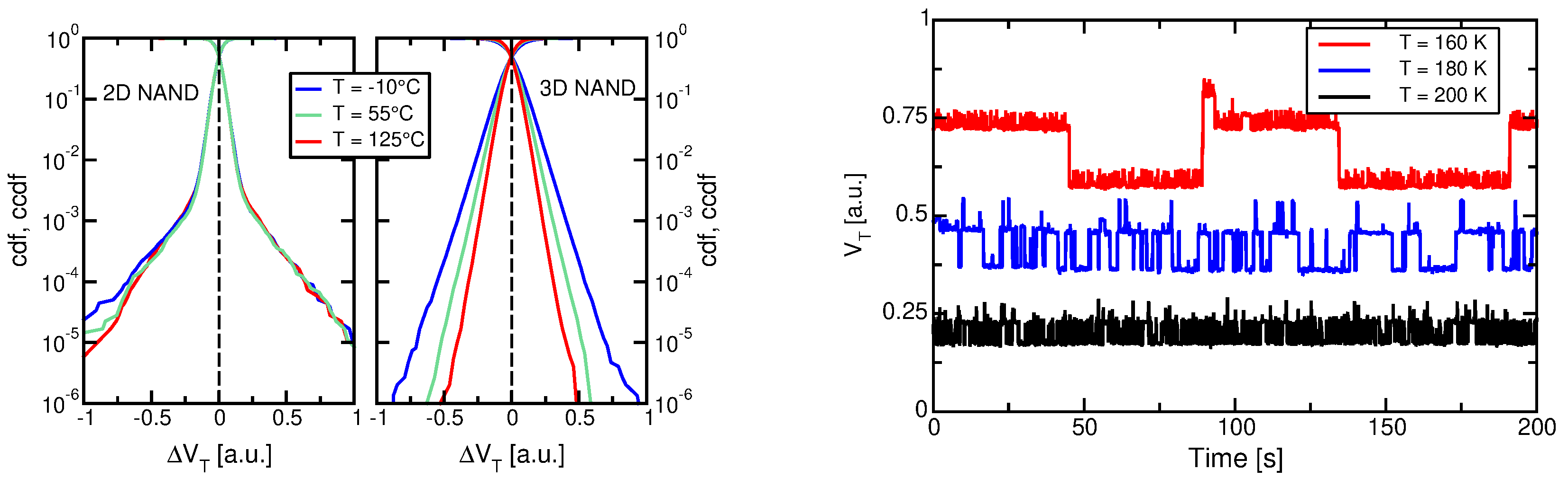
4.2. Array Statistical Data
5. Conclusions
Funding
Acknowledgments
Conflicts of Interest
References
- Ralls, K.S.; Skocpol, W.J.; Jackel, L.D.; Howard, R.E.; Fetter, L.A.; Epworth, R.W.; Tennant, D.M. Discrete resistance switching in submicrometer silicon inversion layers: Individual interface traps and low-frequency (1/f) noise. Phys. Rev. Lett. 1984, 52, 228–231. [Google Scholar] [CrossRef]
- Uren, M.J.; Day, D.J.; Kirton, M.J. 1/f and random telegraph noise in silicon metal-oxide-semiconductor field-effect transistors. Appl. Phys. Lett. 1985, 47, 1195–1197. [Google Scholar] [CrossRef]
- Howard, R.E.; Skocpol, W.J.; Jackel, L.D.; Mankiewich, P.M.; Fetter, L.A.; Tennant, D.M.; Epworth, R.; Ralls, K.S. Single electron switching events in nanometer-scale Si MOSFET’s. IEEE Trans. Electron Devices 1985, 32, 1669–1674. [Google Scholar] [CrossRef]
- Kirton, M.J.; Uren, M.J. Capture and emission kinetics of individual Si:SiO2 interface states. Appl. Phys. Lett. 1986, 48, 1270–1272. [Google Scholar] [CrossRef]
- Hung, K.K.; Ko, P.K.; Hu, C.; Cheng, Y.C. Flicker noise characterization of advanced MOS technologies. In Proceedings of the 1988 International Electron Devices Meeting, San Francisco, CA, USA, 11–14 December 1988; pp. 34–37. [Google Scholar]
- Hung, K.K.; Ko, P.K.; Hu, C.; Cheng, Y.C. Random telegraph noise of deep-submicrometer MOSFET’s. IEEE Electron Device Lett. 1990, 11, 90–92. [Google Scholar] [CrossRef]
- Fang, P.; Hung, K.K.; Ko, P.K.; Hu, C. Hot-electron-induced traps studied through the random telegraph noise. IEEE Electron Device Lett. 1991, 12, 273–275. [Google Scholar] [CrossRef]
- Simoen, E.; Diericks, B.; Claeys, C.L.; Declerck, G.J. Explaining the amplitude of RTS noise in submicrometer MOSFET’s. IEEE Trans. Electron Devices 1992, 39, 422–429. [Google Scholar] [CrossRef]
- Tsai, M.H.; Ma, T.P.; Hook, T.B. Channel length dependence of random telegraph signal in sub-micron MOSFET’s. IEEE Electron Device Lett. 1994, 15, 504–506. [Google Scholar] [CrossRef]
- Uren, M.J.; Kirton, M.J.; Collins, S. Anomalous telegraph noise in small-area silicon metal-oxide-semiconductor field-effect transistors. Phys. Rev. B 1988, 37, 8346–8350. [Google Scholar] [CrossRef]
- Kirton, M.J.; Uren, M.J. Noise in solid-state microstructures: A new perspective on individual defects, interface states and low-frequency (1/f) noise. Adv. Phys. 1989, 38, 367–468. [Google Scholar] [CrossRef]
- Kirton, M.J.; Uren, M.J.; Collins, S.; Schultz, M.; Karmann, A.; Scheffer, K. Individual defects at the Si:SiO2 interface. Semicond. Sci. Technol. 1989, 4, 1116–1126. [Google Scholar] [CrossRef]
- Nakamura, H.; Yasuda, N.; Taniguchi, K.; Hamaguchi, C.; Toriumi, A. Existence of double-charged oxide traps in submicron MOSFET’s. Jpn. J. Appl. Phys. 1989, 28, L2057–L2060. [Google Scholar] [CrossRef]
- Ohata, A.; Toriumi, A.; Iwase, M.; Natori, K. Observation of random telegraph signals: Anomalous nature of defects at the Si/SiO2 interface. J. Appl. Phys. 1990, 68, 200–204. [Google Scholar] [CrossRef]
- Mueller, H.H.; Schulz, M. Conductance modulation of submicrometer metal-oxide-semiconductor field effect transistors by single-electron trapping. J. Appl. Phys. 1996, 79, 4178–4180. [Google Scholar] [CrossRef]
- Mueller, H.H.; Schulz, M. Statistics of random telegraph noise in sub-m MOSFETs. In Proceedings of the 14th International Conference: Noise in Physical Systems and 1/f Fluctuations, Leuven, Belgium, 14–18 July 1997; pp. 195–200. [Google Scholar]
- Kurata, H.; Otsuga, K.; Kotabe, A.; Kajiyama, S.; Osabe, T.; Sasago, Y.; Narumi, S.; Tokami, K.; Kamohara, S.; Tsuchiya, O. The impact of random telegraph signals on the scaling of multilevel Flash memories. In Proceedings of the 2006 Symposium on VLSI Circuits, Honolulu, HI, USA, 15–17 June 2006; pp. 112–113. [Google Scholar]
- Tega, N.; Miki, H.; Osabe, T.; Kotabe, A.; Otsuga, K.; Kurata, H.; Kamohara, S.; Tokami, K.; Ikeda, Y.; Yamada, R. Anomalously large threshold voltage fluctuation by complex random telegraph signal in floating gate Flash memory. In Proceedings of the 2006 International Electron Devices Meeting, San Francisco, CA, USA, 11–13 December 2006; pp. 491–494. [Google Scholar]
- Gusmeroli, R.; Monzio Compagnoni, C.; Riva, A.; Spinelli, A.S.; Lacaita, A.L.; Bonanomi, M.; Visconti, A. Defects spectroscopy in SiO2 by statistical random telegraph noise analysis. In Proceedings of the 2006 International Electron Devices Meeting, San Francisco, CA, USA, 11–13 December 2006; pp. 483–486. [Google Scholar]
- Kurata, H.; Otsuga, K.; Kotabe, A.; Kajiyama, S.; Osabe, T.; Sasago, Y.; Narumi, S.; Tokami, K.; Kamohara, S.; Tsuchiya, O. Random telegraph signal in Flash memory: Its impact on scaling of multilevel Flash memory beyond the 90-nm node. IEEE J. Solid-State Circuits 2007, 42, 1362–1369. [Google Scholar] [CrossRef]
- Fukuda, K.; Shimizu, Y.; Amemiya, K.; Kamoshida, M.; Hu, C. Random telegraph noise in Flash memories—Model and technology scaling. In Proceedings of the 2007 International Electron Devices Meeting, Washington, DC, USA, 10–12 December 2007; pp. 169–172. [Google Scholar]
- Fantini, P.; Ghetti, A.; Marinoni, A.; Ghidini, G.; Visconti, A.; Marmiroli, A. Giant random telegraph signals in nanoscale floating-gate devices. IEEE Electron Device Lett. 2007, 28, 1114–1116. [Google Scholar] [CrossRef]
- Miki, H.; Osabe, T.; Tega, N.; Kotabe, A.; Kurata, H.; Tokami, K.; Ikeda, Y.; Kamohara, S.; Yamada, R. Quantitative analysis of random telegraph signals as fluctuations of threshold voltages in scaled Flash memory cells. In Proceedings of the 2007 IEEE International Reliability Physics Symposium Proceedings—45th Annual, Phoenix, AZ, USA, 15–19 April 2007; pp. 29–35. [Google Scholar]
- Wong, H.S.; Taur, Y. Three-dimensional “atomistic” simulation of discrete random dopant distribution effects in sub-0.1 μm MOSFET’s. In Proceedings of the IEEE International Electron Devices Meeting, Washington, DC, USA, 5–8 December 1993; pp. 705–708. [Google Scholar]
- Asenov, A. Random dopant induced threshold voltage lowering and fluctuations in sub-0.1 μm MOSFET’s: A 3-D “atomistic” simulation study. IEEE Trans. Electron Devices 1998, 45, 2505–2513. [Google Scholar] [CrossRef]
- Asenov, A.; Brown, A.R.; Davies, J.H.; Saini, S. Hierarchical approach to “atomistic” 3-D MOSFET simulation. IEEE Trans. Comput. Aided Des. 1999, 18, 1558–1565. [Google Scholar] [CrossRef]
- Asenov, A.; Saini, S. Suppression of random dopant-induced threshold voltage fluctuations in sub-0.1 μm MOSFET’s with epitaxial and δ-doped channels. IEEE Trans. Electron Devices 1999, 46, 1718–1724. [Google Scholar] [CrossRef]
- Vandamme, L.K.J.; Sodini, D.; Gingl, Z. On the anomalous behavior of the relative amplitude of RTS noise. Solid-State Electron. 1998, 42, 901–905. [Google Scholar] [CrossRef]
- Asenov, A.; Balasubramaniam, R.; Brown, A.R.; Davies, J.H.; Saini, S. Random telegraph signal amplitudes in sub 100 nm (decanano) MOSFETs: A 3D “atomistic” simulation study. In Proceedings of the International Electron Devices Meeting, San Francisco, CA, USA, 10–13 December 2000; pp. 279–282. [Google Scholar]
- Asenov, A.; Balasubramaniam, R.; Brown, A.R.; Davies, J.H. RTS amplitudes in decananometer MOSFETs: 3-D simulation study. IEEE Trans. Electron Devices 2003, 50, 839–845. [Google Scholar] [CrossRef]
- Asenov, A.; Brown, A.R.; Davies, J.H.; Kaya, S.; Slavcheva, G. Simulation of intrinsic parameter fluctuations in decananometer and nanometer-scale MOSFETs. IEEE Trans. Electron Devices 2003, 50, 1837–1852. [Google Scholar] [CrossRef]
- Monzio Compagnoni, C.; Gusmeroli, R.; Spinelli, A.S.; Lacaita, A.L.; Bonanomi, M.; Visconti, A. Statistical model for random telegraph noise in Flash memories. IEEE Trans. Electron Devices 2008, 55, 388–395. [Google Scholar] [CrossRef]
- Ghetti, A.; Monzio Compagnoni, C.; Spinelli, A.S.; Visconti, A. Comprehensive analysis of random telegraph noise instability and its scaling in deca-nanometer Flash memories. IEEE Trans. Electron Devices 2009, 56, 1746–1752. [Google Scholar] [CrossRef]
- Monzio Compagnoni, C.; Castellani, N.; Mauri, A.; Spinelli, A.S.; Lacaita, A.L. Three-dimensional electrostatics- and atomistic doping-induced variability of RTN time constants in nanoscale MOS devices—Part II: Spectroscopic implications. IEEE Trans. Electron Devices 2012, 59, 2495–2500. [Google Scholar] [CrossRef]
- Castellani, N.; Monzio Compagnoni, C.; Mauri, A.; Spinelli, A.S.; Lacaita, A.L. Three-dimensional electrostatics- and atomistic doping-induced variability of RTN time constants in nanoscale MOS devices—Part I: Physical investigation. IEEE Trans. Electron Devices 2012, 59, 2488–2494. [Google Scholar] [CrossRef]
- Adamu-Lema, F.; Monzio Compagnoni, C.; Amoroso, S.M.; Castellani, N.; Gerrer, L.; Markov, S.; Spinelli, A.S.; Lacaita, A.L.; Asenov, A. Accuracy and issues of the spectroscopic analysis of RTN traps in nanoscale MOSFETs. IEEE Trans. Electron Devices 2013, 60, 833–839. [Google Scholar] [CrossRef]
- Spinelli, A.S.; Monzio Compagnoni, C.; Lacaita, A.L. Random telegraph noise in Flash memories. In Noise in Nanoscale Semiconductor Devices; Grasser, T., Ed.; Springer: Berlin, Germany, 2020; Chapter 6; pp. 201–227. [Google Scholar]
- Monzio Compagnoni, C.; Goda, A.; Spinelli, A.S.; Feeley, P.; Lacaita, A.L.; Visconti, A. Reviewing the evolution of the NAND Flash technology. Proc. IEEE 2017, 105, 1609–1633. [Google Scholar] [CrossRef]
- Tanaka, H.; Kido, M.; Yahashi, K.; Oomura, M.; Katsumata, R.; Kito, M.; Fukuzumi, Y.; Sato, M.; Nagata, Y.; Matsuoka, Y.; et al. Bit cost scalable technology with punch and plug process for ultra high density Flash memory. In Proceedings of the 2007 IEEE Symposium on VLSI Technology, Kyoto, Japan, 12–14 June 2007; pp. 14–15. [Google Scholar]
- Fukuzumi, Y.; Katsumata, R.; Kito, M.; Kido, M.; Sato, M.; Tanaka, H.; Nagata, Y.; Matsuoka, Y.; Iwata, Y.; Aochi, H.; et al. Optimal integration and characteristics of vertical array devices for ultra-high density, bit-cost scalable Flash memory. In Proceedings of the International Electron Devices Meeting, San Francisco, CA, USA, 10–12 December 2007; pp. 449–452. [Google Scholar]
- Maeda, T.; Itagaki, K.; Hishida, T.; Katsumata, R.; Kito, M.; Fukuzumi, Y.; Kido, M.; Tanaka, H.; Komori, Y.; Ishiduki, M.; et al. Multi-stacked 1 G cell/layer pipe-shaped BiCS Flash memory. In Proceedings of the 2009 Symposium on VLSI Circuits, Kyoto, Japan, 16–18 June 2009; pp. 22–23. [Google Scholar]
- Ishiduki, M.; Fukuzumi, Y.; Katsumata, R.; Kito, M.; Kido, M.; Tanaka, H.; Komori, Y.; Nagata, Y.; Fujiwara, T.; Maeda, T.; et al. Optimal device structure for pipe-shaped BiCS Flash memory for ultra high density storage device with excellent performance and reliability. In Proceedings of the 2009 IEEE International Electron Devices Meeting, Baltimore, MD, USA, 7–9 December 2009; pp. 625–628. [Google Scholar]
- Katsumata, R.; Kito, M.; Fukuzumi, Y.; Kido, M.; Tanaka, H.; Komori, Y.; Ishiduki, M.; Matsunami, J.; Fujiwara, T.; Nagata, Y.; et al. Pipe-shaped BiCS Flash memory with 16 stacked layers and multi-level-cell operation for ultra high density storage devices. In Proceedings of the 2009 Symposium on VLSI Technology, Kyoto, Japan, 15–17 June 2009; pp. 136–137. [Google Scholar]
- Jang, J.; Kim, H.S.; Cho, W.; Cho, H.; Kim, J.; Shim, S.I.; Jang, Y.; Jeong, J.H.; Son, B.K.; Kim, D.W.; et al. Vertical cell array using TCAT (Terabit Cell Array Transistor) technology for ultra high density NAND Flash memory. In Proceedings of the 2009 Symposium on VLSI Technology, Kyoto, Japan, 15–17 June 2009; pp. 192–193. [Google Scholar]
- Kim, W.; Choi, S.; Sung, J.; Lee, T.; Park, C.; Ko, H.; Jung, J.; Yoo, I.; Park, Y. Multi-layered vertical gate NAND Flash overcoming stacking limit for terabit density storage. In Proceedings of the 2009 Symposium on VLSI Technology, Kyoto, Japan, 15–17 June 2009; pp. 188–189. [Google Scholar]
- Lue, H.T.; Chen, S.H.; Shih, Y.H.; Hsieh, K.Y.; Lu, C.Y. Overview of 3D NAND Flash and progress of vertical gate (VG) architecture. In Proceedings of the 2012 IEEE 11th International Conference on Solid-State and Integrated Circuit Technology, Xi’an, China, 29 October–1 November 2012; pp. 914–917. [Google Scholar]
- Tanaka, T.; Helm, M.; Vali, T.; Ghodsi, R.; Kawai, K.; Park, J.K.; Yamada, S.; Pan, F.; Einaga, Y.; Ghalam, A.; et al. A 768Gb 3b/cell 3D-floating-gate NAND Flash memory. In Proceedings of the 2016 IEEE International Solid-State Circuits Conference, San Francisco, CA, USA, 31 January–4 February 2016; pp. 142–143. [Google Scholar]
- Parat, K.; Goda, A. Scaling trends in NAND Flash. In Proceedings of the 2018 IEEE International Electron Devices Meeting, San Francisco, CA, USA, 1–5 December 2018; pp. 27–30. [Google Scholar]
- Siau, C.; Kim, K.H.; Lee, S.; Isobe, K.; Shibata, N.; Verma, K.; Ariki, T.; Li, J.; Yuh, J.; Amarnath, A.; et al. A 512Gb 3-bit/cell 3D Flash memory on 128-wordline-layer with 132MB/s write performance featuring circuit-under-array technology. In Proceedings of the 2019 IEEE International Solid-State Circuits Conference, San Francisco, CA, USA, 17–21 February 2019; pp. 218–220. [Google Scholar]
- Kim, D.H.; Kim, H.; Yun, S.; Song, Y.; Kim, J.; Joe, S.M.; Kang, K.H.; Jang, J.; Yoon, H.J.; Lee, K.; et al. A 1Tb 4 b/cell NAND Flash memory with tPROG = 2 ms, tR = 110 μs and 1.2 Gb/s high-speed IO rate. In Proceedings of the 2020 IEEE International Solid-State Circuits Conference, San Francisco, CA, USA, 16–20 February 2020. [Google Scholar]
- Micheloni, R. (Ed.) 3D Flash Memories; Springer: Berlin, Germany, 2016. [Google Scholar]
- Spinelli, A.S.; Monzio Compagnoni, C.; Lacaita, A.L. Reliability of NAND Flash memories: Planar cells and emerging issues in 3D devices. Computers 2017, 6, 16. [Google Scholar] [CrossRef]
- Monzio Compagnoni, C.; Spinelli, A.S. Reliability of NAND Flash arrays: A review of what the 2-D-to-3-D transition meant. IEEE Trans. Electron Devices 2019, 66, 4504–4516. [Google Scholar] [CrossRef]
- Goda, A. 3D NAND technology achievements and future scaling perspectives. IEEE Trans. Electron Devices 2020, 67, 1373–1381. [Google Scholar] [CrossRef]
- Whang, S.; Lee, K.; Shin, D.; Kim, B.; Kim, M.; Bin, J.; Han, J.; Kim, S.; Lee, B.; Jung, Y.; et al. Novel 3-Dimensional dual control-gate with surrounding floating-gate (DC-SF) NAND Flash cell for 1Tb file storage application. In Proceedings of the 2010 International Electron Devices Meeting, San Francisco, CA, USA, 6–8 December 2010; pp. 668–671. [Google Scholar]
- Noh, Y.; Ahn, Y.; Yoo, H.; Han, B.; Chung, S.; Shim, K.; Lee, K.; Kwak, S.; Shin, S.; Choi, I.; et al. A new metal control gate last process (MCGL process) for high performance DC-SF (dual control gate with surrounding floating gate) 3D NAND Flash memory. In Proceedings of the 2012 Symposium on VLSI Technology (VLSIT), Honolulu, HI, USA, 12–14 June 2012; pp. 19–20. [Google Scholar]
- Aritome, S.; Whang, S.; Lee, K.; Shin, D.; Kim, B.; Kim, M.; Bin, J.; Han, J.; Kim, S.; Lee, B.; et al. A novel three-dimensional dual control-gate with surrounding floating-gate (DC-SF) NAND flash cell. Solid-State Electron. 2013, 79, 166–171. [Google Scholar] [CrossRef]
- Aritome, S.; Noh, Y.; Yoo, H.; Choi, E.S.; Joo, H.S.; Ahn, Y.; Han, B.; Chung, S.; Shim, K.; Lee, K.; et al. Advanced DC-SF cell technology for 3-D NAND Flash. IEEE Trans. Electron Devices 2013, 60, 1327–1333. [Google Scholar] [CrossRef]
- Parat, K.; Dennison, C. A floating gate based 3-D NAND technology with CMOS under array. In Proceedings of the 2015 IEEE International Electron Devices Meeting, Washington, DC, USA, 7–9 December 2015; pp. 48–51. [Google Scholar]
- Sako, M.; Watanabe, Y.; Nakajima, T.; Sato, J.; Muraoka, K.; Fujiu, M.; Kouno, F.; Nakagawa, M.; Masuda, M.; Kato, K.; et al. A low-power 64 Gb MLC NAND-Flash memory in 15 nm CMOS technology. IEEE J. Solid-State Circuits 2015, 51, 128–129. [Google Scholar]
- Park, K.T.; Nam, S.; Kim, D.; Kwak, P.; Lee, D.; Choi, Y.H.; Choi, M.H.; Kwak, D.H.; Kim, D.H.; Kim, M.S.; et al. Three-dimensional 128 Gb MLC vertical NAND Flash memory with 24-WL stacked layers and 50 MB/s high-speed programming. IEEE J. Solid-State Circuits 2015, 50, 204–213. [Google Scholar] [CrossRef]
- Kang, D.; Jeong, W.; Kim, C.; Kim, D.H.; Cho, Y.S.; Kang, K.T.; Ryu, J.; Kang, K.M.; Lee, S.; Kim, W.; et al. 256 Gb 3 b/cell V-NAND Flash memory with 48 stacked WL layers. IEEE J. Solid-State Circuits 2016, 52, 210–217. [Google Scholar] [CrossRef]
- Lee, S.; Lee, J.; Park, I.; Park, J.; Yun, S.; Kim, M.; Lee, J.; Kim, M.; Lee, K.; Kim, T.; et al. A 128 Gb 2 b/cell NAND Flash memory in 14nm technology with tPROG = 640 s and 800 MB/s I/O rate. In Proceedings of the 2016 IEEE International Solid-State Circuits Conference, San Francisco, CA, USA, 31 January–4 February 2016; pp. 138–139. [Google Scholar]
- Lee, S.; Kim, C.; Kim, M.; Joe, S.; Jang, J.; Kim, S.; Lee, K.; Kim, J.; Park, J.; Lee, H.J.; et al. A 1 Tb 4 b/cell 64-stacked-WL 3D NAND flash memory with 12 MB/s program throughput. In Proceedings of the 2018 IEEE International Solid-State Circuits Conference, San Francisco, CA, USA, 11–15 February 2018; pp. 340–342. [Google Scholar]
- Seager, C.H. Grain boundaries in polycrystalline silicon. Ann. Rev. Mater. Sci. 1985, 15, 271–302. [Google Scholar] [CrossRef]
- Jackson, W.B.; Johnson, N.M.; Biegelsen, D.K. Density of gap states of silicon grain boundaries determined by optical absorption. Appl. Phys. Lett. 1983, 43, 195–197. [Google Scholar] [CrossRef]
- Werner, J.; Peisl, M. Exponential band tails in polycrystalline semiconductor films. Phys. Rev. B 1985, 31, 6681–6683. [Google Scholar] [CrossRef]
- Fortunato, G.; Migliorato, P. Determination of gap state density in polycrystalline silicon by field-effect conductance. Appl. Phys. Lett. 1986, 49, 1025–1027. [Google Scholar] [CrossRef]
- Evans, P.V.; Nelson, S.F. Determination of grain-boundary defect-state densities from transport measurements. J. Appl. Phys. 1991, 69, 3605–3611. [Google Scholar] [CrossRef]
- Kimura, M.; Nozawa, R.; Inoue, S.; Shimoda, T.; Lui, B.O.K.; Tam, S.W.B.; Migliorato, P. Extraction of trap states at the oxide-silicon interface and grain boundary for polycrystalline silicon thin-film transistors. Jpn. J. Appl. Phys. 2001, 40, 5227–5236. [Google Scholar] [CrossRef]
- Ikeda, H. Evaluation of grain boundary trap states in polycrystalline-silicon thin-film transistors by mobility and capacitance measurements. J. Appl. Phys. 2002, 91, 4637–4645. [Google Scholar] [CrossRef]
- Hastas, N.A.; Tassis, D.H.; Dimitriadis, C.A.; Kamarinos, G. Determination of interface and bulk traps in the subthreshold region of polycrystalline silicon thin-film transistors. IEEE Trans. Electron Devices 2003, 50, 1991–1994. [Google Scholar] [CrossRef]
- Kimura, M. Extraction of trap densities in entire bandgap of poly-Si thin-film transistors fabricated by solid-phase crystallization and dependence on process conditions of post annealing. Solid-State Electron. 2011, 63, 94–99. [Google Scholar] [CrossRef]
- Wei, X.; Deng, W.; Fang, J.; Ma, X.; Huang, J. Determination of bulk and interface density of states in metal oxide semiconductor thin-film transistors by using capacitance–voltage characteristics. Eur. Phys. J. Appl. Phys. 2017, 80, 10103. [Google Scholar] [CrossRef]
- Hack, M.; Shaw, J.G.; LeComber, P.G.; Willums, M. Numerical simulations of amorphous and polycrystalline silicon thin-film transistors. Jpn. J. Appl. Phys. 1990, 29, 2360–2362. [Google Scholar] [CrossRef]
- Jacunski, M.D.; Shur, M.S.; Hack, M. Threshold voltage, field effect mobility, and gate-to-channel capacitance in polysilicon TFTs. IEEE Trans. Electron Devices 1996, 43, 1433–1440. [Google Scholar] [CrossRef]
- Valdinoci, M.; Colalongo, L.; Baccarani, G.; Pecora, A.; Policicchio, I.; Fortunato, G.; Plais, F.; Legagneux, P.; Reita, C.; Priba, D. Analysis of electrical characteristics of polycrystalline silicon thin-film transistors under static and dynamic conditions. Solid-State Electron. 1997, 41, 1363–1369. [Google Scholar] [CrossRef]
- Chow, T.; Wong, M. An analytical model for the transfer characteristics of a polycrystalline silicon thin-film transistor with a double exponential grain-boundary trap-state energy dispersion. IEEE Electron Dev. Lett. 2009, 30, 1072–1074. [Google Scholar] [CrossRef]
- Amit, I.; Englander, D.; Horvitz, D.; Sasson, Y.; Rosenwaks, Y. Density and energy distribution of interface states in the grain boundaries of polysilicon nanowire. Nano Lett. 2014, 14, 6190–6194. [Google Scholar] [CrossRef]
- Peisl, M.; Wieder, A.W. Conductivity in polycrystalline silicon—Physics and rigorous numerical treatment. IEEE Trans. Electron Devices 1983, 30, 1792–1797. [Google Scholar] [CrossRef]
- Kim, D.M.; Khondker, A.; Ahmed, S.S.; Shah, R.R. Theory of conduction in polysilicon: Drift-diffusion approach in crystalline-amorphous-crystalline semiconductor system—Part I: Small signal theory. IEEE Trans. Electron Devices 1984, 31, 480–493. [Google Scholar] [CrossRef]
- Khondker, A.N.; Kim, D.M.; Ahmed, S.S.; Shah, R.R. Theory of conduction in polysilicon: Drift-diffusion approach in crystalline-amorphous-crystalline semiconductor system—Part II: General I-V theory. IEEE Trans. Electron Devices 1984, 31, 493–500. [Google Scholar] [CrossRef]
- Seto, J.Y.W. The electrical properties of polycrystalline silicon films. J. Appl. Phys. 1975, 46, 5247–5254. [Google Scholar] [CrossRef]
- Baccarani, G.; Riccò, B.; Spadini, G. Transport properties of polycrystalline silicon films. J. Appl. Phys. 1978, 49, 5565–5570. [Google Scholar] [CrossRef]
- Mandurah, M.M.; Saraswat, K.C.; Kamins, T.I. A model for conduction in polycrystalline silicon—Part I: Theory. IEEE Trans. Electron Devices 1981, 28, 1163–1171. [Google Scholar] [CrossRef]
- Lu, N.C.C.; Gerzberg, L.; Lu, C.Y.; Meindl, J.D. Modeling and optimization of monolithic polycrystalline silicon resistors. IEEE Trans. Electron Devices 1981, 28, 818–830. [Google Scholar] [CrossRef]
- Lee, J.Y.; Wang, F.Y. Temperature dependence of carrier trnsport in polycrystalline silicon. Microelectron. J. 1986, 17, 23–32. [Google Scholar] [CrossRef]
- Mannara, A.; Spinelli, A.S.; Lacaita, A.L.; Monzio Compagnoni, C. Current transport in polysilicon-channel GAA MOSFETs: A modeling perspective. In Proceedings of the 49th European Solid-State Device Research Conference (ESSDERC), Cracow, Poland, 23–26 September 2019; pp. 222–225. [Google Scholar]
- Mannara, A.; Malavena, G.; Spinelli, A.S.; Monzio Compagnoni, C. A comparison of modeling approaches for current transport in polysilicon-channel nanowire and macaroni GAA MOSFETs. J. Comp. Electr. 2021, 20, 537–544. [Google Scholar] [CrossRef]
- Hsiao, Y.H.; Lue, H.T.; Chen, W.C.; Chen, C.P.; Chang, K.P.; Shih, Y.H.; Tsui, B.Y.; Lu, C.Y. Modeling the variability caused by random grain boundary and trap-location induced asymmetrical read behavior for a tight-pitch vertical gate 3D NAND Flash memory using double-gate thin-film transistor (TFT) device. In Proceedings of the 2012 International Electron Devices Meeting, San Francisco, CA, USA, 10–13 December 2012; pp. 609–612. [Google Scholar]
- Hsiao, Y.H.; Lue, H.T.; Chen, W.C.; Chang, K.P.; Shih, Y.H.; Tsui, B.Y.; Hsieh, K.Y.; Lu, C.Y. Modeling the impact of random grain boundary traps on the electrical behavior of vertical gate 3-D NAND Flash memory devices. IEEE Trans. Electron Devices 2014, 61, 2064–2070. [Google Scholar] [CrossRef]
- Yang, C.W.; Su, P. Simulation and investigation of random grain-boundary-induced variabilities for stackable NAND Flash using 3-D Voronoi grain patterns. IEEE Trans. Electron Devices 2014, 61, 1211–1214. [Google Scholar] [CrossRef]
- Kim, J.; Lee, J.; Oh, H.; Rim, T.; Baek, C.K.; Meyyappan, M.; Lee, J.S. The variability due to random discrete dopant and grain boundary in 3D NAND unit cell. In Proceedings of the 2014 IEEE International Nanoelectronics Conference (INEC), Sapporo, Japan, 28–31 July 2014; pp. 66–68. [Google Scholar]
- Wang, P.Y.; Tsui, B.Y. A novel approach using discrete grain-boundary traps to study the variability of 3-D vertical-gate NAND Flash memory cells. IEEE Trans. Electron Devices 2015, 62, 2488–2493. [Google Scholar] [CrossRef]
- Degraeve, R.; Clima, S.; Putcha, V.; Kaczer, B.; Roussel, P.; Linten, D.; Groeseneken, G.; Arreghini, A.; Karner, M.; Kernstock, C.; et al. Statistical poly-Si grain boundary model with discrete charging defects and its 2D and 3D implementation for vertical 3D NAND channels. In Proceedings of the 2015 IEEE International Electron Devices Meeting, Washington, DC, USA, 7–9 December 2015; pp. 121–124. [Google Scholar]
- Lun, Z.; Shen, L.; Cong, Y.; Du, G.; Liu, X.; Wang, Y. Investigation of the impact of grain boundary on threshold voltage of 3-D MLC NAND Flash memory. In Proceedings of the 2015 Silicon Nanoelectronics Workshop (SNW), Kyoto, Japan, 14–15 June 2015; pp. 35–37. [Google Scholar]
- Oh, H.; Kim, J.; Lee, J.; Rim, T.; Baek, C.K.; Lee, J.S. Effects of single grain boundary and random interface traps on electrical variations of sub-30 nm polysilicon nanowire structures. Microelectron. Eng. 2016, 149, 113–116. [Google Scholar] [CrossRef]
- Resnati, D.; Mannara, A.; Nicosia, G.; Paolucci, G.M.; Tessariol, P.; Lacaita, A.L.; Spinelli, A.S.; Monzio Compagnoni, C. Temperature activation of the string current and its variability in 3-D NAND Flash arrays. In Proceedings of the 2017 IEEE International Electron Devices Meeting, San Francisco, CA, USA, 2–6 December 2017; pp. 103–106. [Google Scholar]
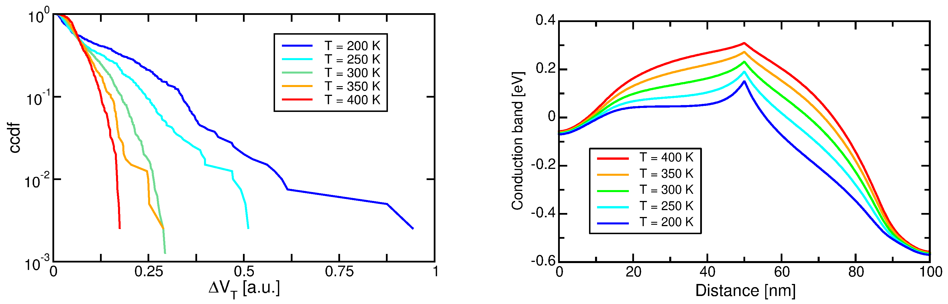
- Nicosia, G.; Mannara, A.; Resnati, D.; Paolucci, G.M.; Tessariol, P.; Lacaita, A.L.; Spinelli, A.S.; Goda, A.; Monzio Compagnoni, C. Inpact of temperature on the amplitude of RTN fluctuations in 3-D NAND Flash cells. In Proceedings of the 2017 IEEE International Electron Devices Meeting, San Francisco, CA, USA, 2–6 December 2017; pp. 521–524. [Google Scholar]
- Resnati, D.; Mannara, A.; Nicosia, G.; Paolucci, G.M.; Tessariol, P.; Spinelli, A.S.; Lacaita, A.L.; Monzio Compagnoni, C. Characterization and modeling of temperature effects in 3-D NAND Flash arrays—Part I: Polysilicon-induced variability. IEEE Trans. Electron Devices 2018, 65, 3199–3206. [Google Scholar] [CrossRef]
- Nicosia, G.; Mannara, A.; Resnati, D.; Paolucci, G.M.; Tessariol, P.; Spinelli, A.S.; Lacaita, A.L.; Goda, A.; Monzio Compagnoni, C. Characterization and modeling of temperature effects in 3-D NAND Flash arrays—Part II: Random telegraph noise. IEEE Trans. Electron Devices 2018, 65, 3207–3213. [Google Scholar] [CrossRef]
- Verreck, D.; Arreghini, A.; Schanovsky, F.; Stanojević, Z.; Steiner, K.; Mitterbauer, F.; Karner, M.; den Bosch, G.V.; Furnémont, A. 3D TCAD model for poly-Si channel current and variability in vertical NAND Flash memory. In Proceedings of the 2019 International Conference on Simulation of Semiconductor Processes and Devices (SISPAD), Udine, Italy, 4–6 September 2019; pp. 61–64. [Google Scholar]
- Degraeve, R.; Toledano-Luque, M.; Arreghini, A.; Tang, B.; Capogreco, E.; Lisoni, J.; Roussel, P.; Kaczer, B.; Van den bosch, G.; Groeseneken, G.; et al. Characterizing grain size and defect energy distribution in vertical SONOS poly-Si channels by means of a resistive network model. In Proceedings of the 2013 IEEE International Electron Devices Meeting, Washington, DC, USA, 9–11 December 2013; pp. 558–561. [Google Scholar]
- Yoo, W.S.; Ishigaki, T.; Ueda, T.; Kang, K.; Kwak, N.Y.; Sheen, D.S.; Kim, S.S.; Ko, M.S.; Shin, W.S.; Lee, B.S.; et al. Grain size monitoring of 3D Flash memory channel poly-Si using multiwavelength Raman spectroscopy. In Proceedings of the 2014 14th Annual Non-Volatile Memory Technology Symposium (NVMTS), Jeju, Korea, 27–29 October 2014; pp. 44–47. [Google Scholar]
- Kim, S.Y.; Park, J.K.; Hwang, W.S.; Lee, S.J.; Lee, K.H.; Pyi, S.H.; Cho, B.J. Dependence of grain size on the performance of a polysilicon channel TFT for 3D NAND Flash memory. J. Nanosci. Nanotechnol. 2016, 16, 5044–5048. [Google Scholar] [CrossRef] [PubMed]
- He, D.; Okada, N.; Fortmann, C.M.; Shimizu, I. Carrier transport in polycrystalline silicon films deposited by a layer-by-layer technique. J. Appl. Phys. 1994, 76, 4728–4733. [Google Scholar] [CrossRef]
- Walker, A.J.; Herner, S.B.; Kumar, T.; Chen, E.H. On the conduction mechanism in polycrystalline silicon thin-film transistors. IEEE Trans. Electron Devices 2004, 51, 1856–1866. [Google Scholar] [CrossRef]
- Jeong, M.K.; Joe, S.M.; Seo, C.S.; Han, K.R.; Choi, E.; Park, S.K.; Lee, J.H. Analysis of random telegraph noise and low frequency noise properties in 3-D stacked NAND Flash memory with tube-type poly-Si channel structure. In Proceedings of the 2012 Symposium on VLSI Technology (VLSIT), Honolulu, HI, USA, 12–14 June 2012; pp. 55–56. [Google Scholar]
- Jeong, M.K.; Joe, S.M.; Jo, B.S.; Kang, H.J.; Bae, J.H.; Han, K.R.; Choi, E.; Cho, G.; Park, S.K.; Park, B.G.; et al. Characterization of traps in 3-D stacked NAND Flash memory devices with tube-type poly-Si channel structure. In Proceedings of the 2012 International Electron Devices Meeting, San Francisco, CA, USA, 10–13 December 2012. [Google Scholar]
- Kang, D.; Lee, C.; Hur, S.; Song, D.; Choi, J.H. A new approach for trap analysis of vertical NAND Flash cell using RTN characteristics. In Proceedings of the 2014 IEEE International Electron Devices Meeting, San Francisco, CA, USA, 15–17 December 2014; pp. 367–370. [Google Scholar]
- Amoroso, S.M.; Monzio Compagnoni, C.; Ghetti, A.; Gerrer, L.; Spinelli, A.S.; Lacaita, A.L.; Asenov, A. Investigation of the RTN distribution of nanoscale MOS devices from subthreshold to on-state. IEEE Electron Device Lett. 2013, 34, 683–685. [Google Scholar] [CrossRef]
- Saraza-Canflanca, P.; Martin-Martinez, J.; Castro-Lopez, R.; Roca, E.; Rodriguez, R.; Nafria, M.; Fernandez, F.V. A detailed study of the gate/drain voltage dependence of RTN in bulk pMOS transistors. Microelectron. Eng. 2019, 215, 111004. [Google Scholar] [CrossRef]
- Spinelli, A.S.; Monzio Compagnoni, C.; Lacaita, A.L. Variability effects in nanowire and macaroni MOSFETs—Part II: Random telegraph noise. IEEE Trans. Electron Devices 2020, 67, 1492–1497. [Google Scholar] [CrossRef]
- Andrade, M.; Toledano-Luque, M.; Fourati, F.; Degraeve, R.; Martino, J.; Claeys, C.; Simoen, E.; Van den bosch, G.; Van Houdt, J. RTN assessment of traps in polysilicon cylindrical vertical FETs for NVM application. Microelectron. Eng. 2013, 109, 105–108. [Google Scholar] [CrossRef]
- Toledano-Luque, M.; Degraeve, R.; Roussel, P.J.; Luong, V.; Tang, B.; Lisoni, J.G.; Tan, C.L.; Arreghini, A.; Van den bosch, G.; Groeseneken, G.; et al. Statistical spectroscopy of switching traps in deeply scaled vertical poly-Si channel for 3D memories. In Proceedings of the 2013 IEEE International Electron Devices Meeting, Washington, DC, USA, 9–11 December 2013; pp. 562–565. [Google Scholar]
- Lee, C.M.; Tsui, B.Y. Random telegraph signal noise arising from grain boundary traps in nano-scale poly-Si nanowire thin-film transistors. In Proceedings of the 2013 International Symposium on VLSI Technology, Systems and Application (VLSI-TSA), Hsinchu, Taiwan, 22–24 April 2013; pp. 47–48. [Google Scholar]
- Nicosia, G.; Goda, A.; Spinelli, A.S.; Monzio Compagnoni, C. Investigation of the temperature dependence of random telegraph noise fluctuations in nanoscale polysilicon-channel 3-D Flash cells. Solid-State Electron. 2019, 151, 18–22. [Google Scholar] [CrossRef]
- Degraeve, R.; Toledano-Luque, M.; Suhane, A.; Van den bosch, G.; Arreghini, A.; Tang, B.; Kaczer, B.; Roussel, P.; Kar, G.S.; Van Houdt, J.; et al. Statistical characterization of current paths in narrow poly-Si channels. In Proceedings of the 2011 International Electron Devices Meeting, Washington, DC, USA, 5–7 December 2011; pp. 287–290. [Google Scholar]
- Nowak, E.; Kim, J.H.; Kwon, H.; Kim, Y.G.; Sim, J.S.; Lim, S.H.; Kim, D.S.; Lee, K.H.; Park, Y.K.; Choi, J.H.; et al. Intrinsic fluctuations in vertical NAND Flash memories. In Proceedings of the 2012 Symposium on VLSI Technology (VLSIT), Honolulu, HI, USA, 12–14 June 2012; pp. 21–22. [Google Scholar]
- Toledano-Luque, M.; Degraeve, R.; Kaczer, B.; Tang, B.; Roussel, P.J.; Weckx, P.; Franco, J.; Arreghini, A.; Suhane, A.; Kar, G.S.; et al. Quantitative and predictive model of reading current variability in deeply scaled vertical poly-Si channel for 3D memories. In Proceedings of the 2012 International Electron Devices Meeting, San Francisco, CA, USA, 10–13 December 2012. [Google Scholar]
- Goda, A.; Miccoli, C.; Monzio Compagnoni, C. Time dependent threshold-voltage fluctuations in NAND Flash memories: From basic physics to impact on array operation. In Proceedings of the 2015 IEEE International Electron Devices Meeting, Washington, DC, USA, 7–9 December 2015; pp. 374–377. [Google Scholar]
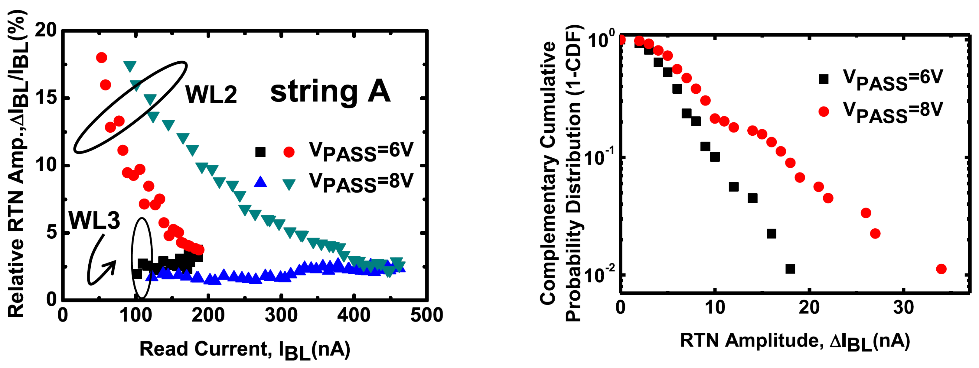
- Chou, Y.L.; Wang, T.; Lin, M.; Chang, Y.W.; Liu, L.; Huang, S.W.; Tsai, W.J.; Lu, T.C.; Chen, K.C.; Lu, C.Y. Poly-silicon trap position and pass voltage effects on RTN amplitude in a vertical NAND Flash cell string. IEEE Electron Dev. Lett. 2016, 37, 998–1001. [Google Scholar] [CrossRef]
- Hsieh, C.C.; Lue, H.T.; Hsu, T.H.; Du, P.Y.; Chiang, K.H.; Lu, C.Y. A Monte Carlo simulation method to predict large-density NAND product memory window from small-array test element group (TEG) verified on a 3D NAND Flash test chip. In Proceedings of the 2016 IEEE Symposium on VLSI Technology, Honolulu, HI, USA, 14–16 June 2016; pp. 63–64. [Google Scholar]
- Hung, C.H.; Lue, H.T.; Hung, S.N.; Hsieh, C.C.; Chang, K.P.; Chen, T.W.; Huang, S.L.; Chen, T.S.; Chang, C.S.; Yeh, W.W.; et al. Design innovations to optimize the 3D stackable vertical gate (VG) NAND Flash. In Proceedings of the 2012 International Electron Devices Meeting, San Francisco, CA, USA, 10–13 December 2012; pp. 227–230. [Google Scholar]
- Resnati, D.; Goda, A.; Nicosia, G.; Miccoli, C.; Spinelli, A.S.; Monzio Compagnoni, C. Temperature effects in NAND Flash memories: A comparison between 2-D and 3-D arrays. IEEE Electron Dev. Lett. 2017, 38, 461–464. [Google Scholar] [CrossRef]
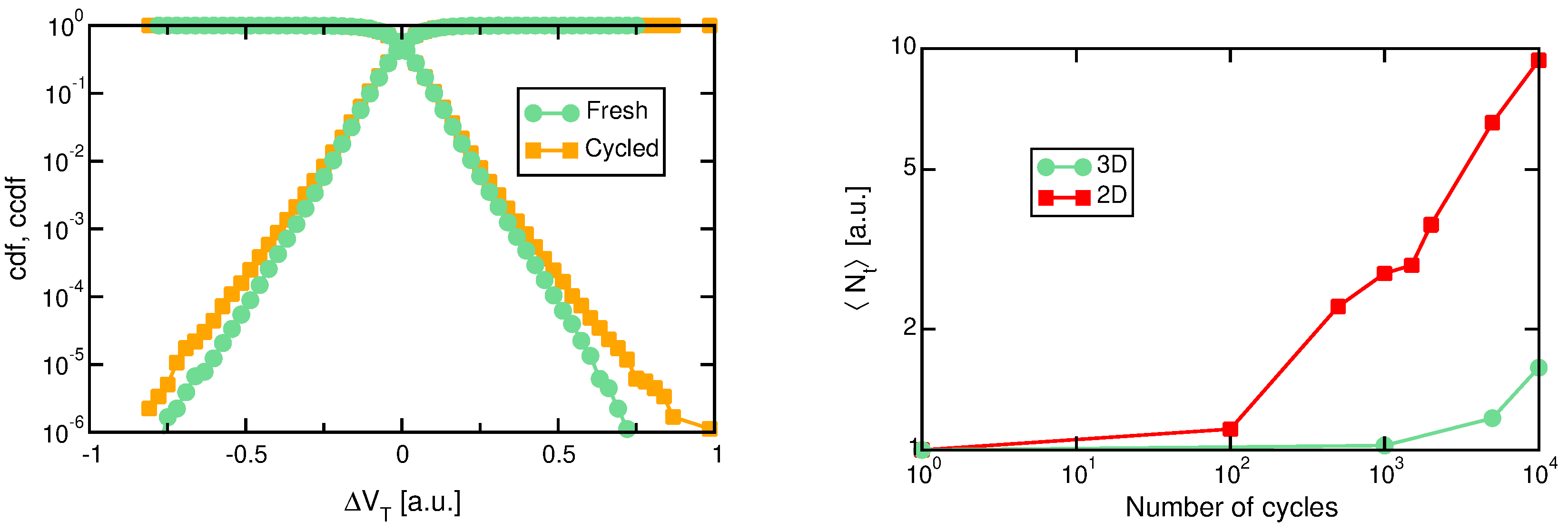
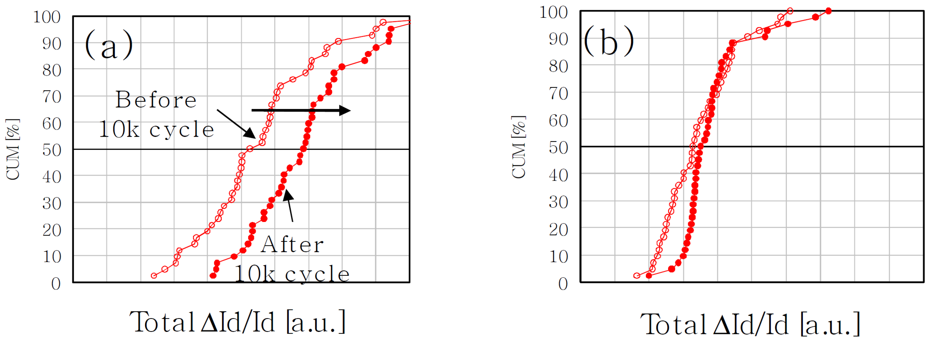
- Nicosia, G.; Goda, A.; Spinelli, A.S.; Monzio Compagnoni, C. Impact of cycling on random telegraph noise in 3-D NAND Flash arrays. IEEE Electron Dev. Lett. 2018, 39, 1175–1178. [Google Scholar] [CrossRef]
- Cappelletti, P. Non volatile memory evolution and revolution. In Proceedings of the 2015 IEEE International Electron Devices, Washington, DC, USA, 7–9 December 2015; pp. 241–244. [Google Scholar]
- Miccoli, C.; Paolucci, G.M.; Monzio Compagnoni, C.; Spinelli, A.S.; Goda, A. Cycling pattern and read/bake conditions dependence of random telegraph noise in decananometer NAND Flash arrays. In Proceedings of the 2015 IEEE International Reliability Physics Symposium, Monterey, CA, USA, 19–23 April 2015; pp. MY.9.1–MY.9.4. [Google Scholar]
- Monzio Compagnoni, C.; Spinelli, A.S.; Beltrami, S.; Bonanomi, M.; Visconti, A. Cycling effect on the random telegraph noise instabilities of NOR and NAND Flash arrays. IEEE Electron Device Lett. 2008, 29, 941–943. [Google Scholar] [CrossRef]
- Monzio Compagnoni, C.; Gusmeroli, R.; Spinelli, A.S.; Lacaita, A.L.; Bonanomi, M.; Visconti, A. Statistical investigation of random telegraph noise ID instabilities in Flash cells at different initial trap-filling conditions. In Proceedings of the 2007 45th Annual IEEE International Reliability Physics Symposium Proceedings, Phoenix, AZ, USA, 15–19 April 2007; pp. 161–166. [Google Scholar]
- Choi, N.; Kang, H.J.; Lee, J.H. Analysis of random telegraph noise characteristics with two different cell states in 3-D NAND Flash memory. J. Semicond. Technol. Sci. 2019, 19, 153–157. [Google Scholar] [CrossRef]


| [cm eV ] | [meV] | [cm eV ] | [meV] |
|---|---|---|---|
| – | 16.6–80 | –9 | 80–500 |
Publisher’s Note: MDPI stays neutral with regard to jurisdictional claims in published maps and institutional affiliations. |
© 2021 by the authors. Licensee MDPI, Basel, Switzerland. This article is an open access article distributed under the terms and conditions of the Creative Commons Attribution (CC BY) license (https://creativecommons.org/licenses/by/4.0/).
Share and Cite
Spinelli, A.S.; Malavena, G.; Lacaita, A.L.; Monzio Compagnoni, C. Random Telegraph Noise in 3D NAND Flash Memories. Micromachines 2021, 12, 703. https://doi.org/10.3390/mi12060703
Spinelli AS, Malavena G, Lacaita AL, Monzio Compagnoni C. Random Telegraph Noise in 3D NAND Flash Memories. Micromachines. 2021; 12(6):703. https://doi.org/10.3390/mi12060703
Chicago/Turabian StyleSpinelli, Alessandro S., Gerardo Malavena, Andrea L. Lacaita, and Christian Monzio Compagnoni. 2021. "Random Telegraph Noise in 3D NAND Flash Memories" Micromachines 12, no. 6: 703. https://doi.org/10.3390/mi12060703
APA StyleSpinelli, A. S., Malavena, G., Lacaita, A. L., & Monzio Compagnoni, C. (2021). Random Telegraph Noise in 3D NAND Flash Memories. Micromachines, 12(6), 703. https://doi.org/10.3390/mi12060703