
Self-Consistent Enhanced S/D Tunneling Implementation in a 2D MS-EMC Nanodevice Simulator

 ,
,  ,
,  , , ,
, , ,  and
and 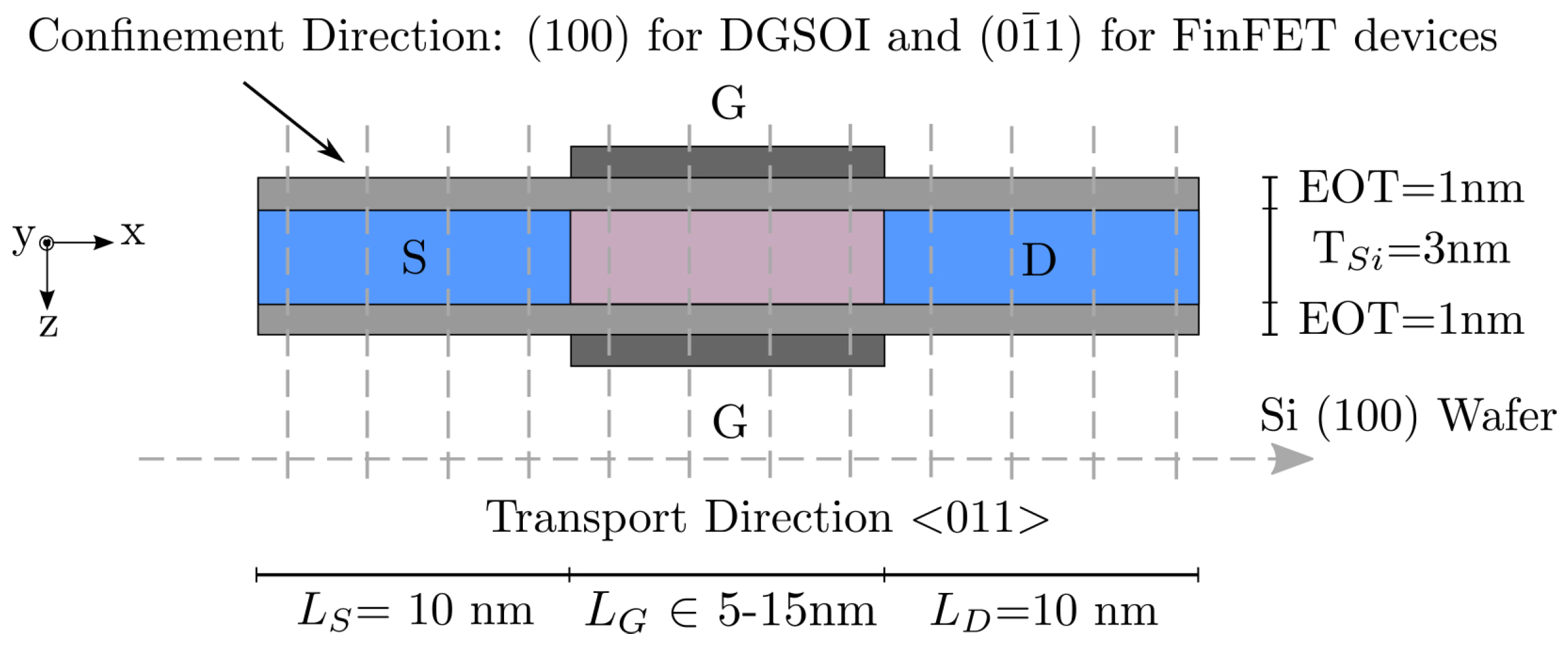
Abstract
1. Introduction
2. Simulation Framework and Device Structures
2.1. Description of the Simulated Devices
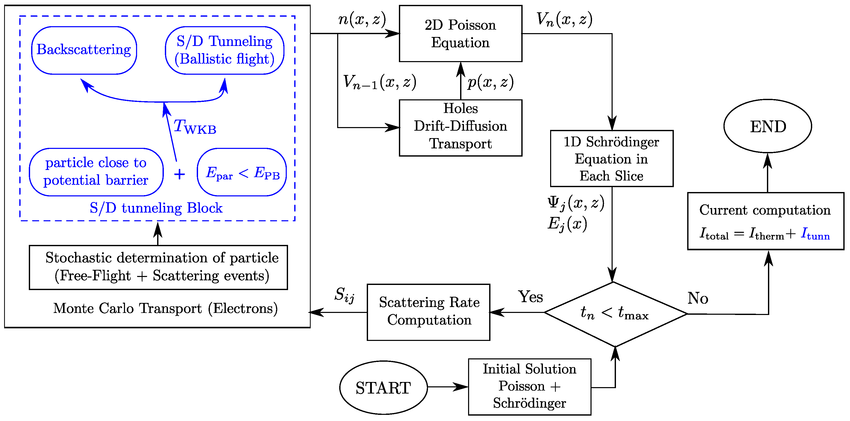
2.2. General Overview of the 2D MS-EMC Tool
2.3. S/D Tunneling Implementation inside the 2D MC-EMC Tool
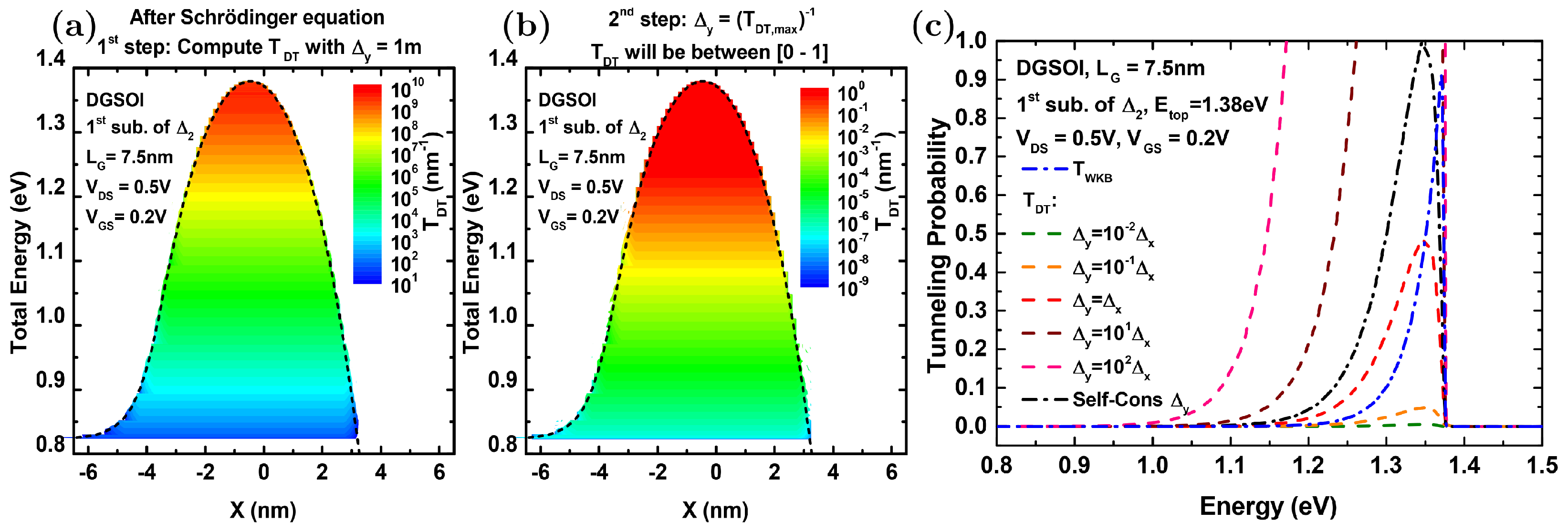
2.3.1. Standpoint 1. Reformulation of the Tunneling Probability
2.3.2. Standpoint 2. Tunneling Current Computation by Means of the Landauer Formula
3. Results
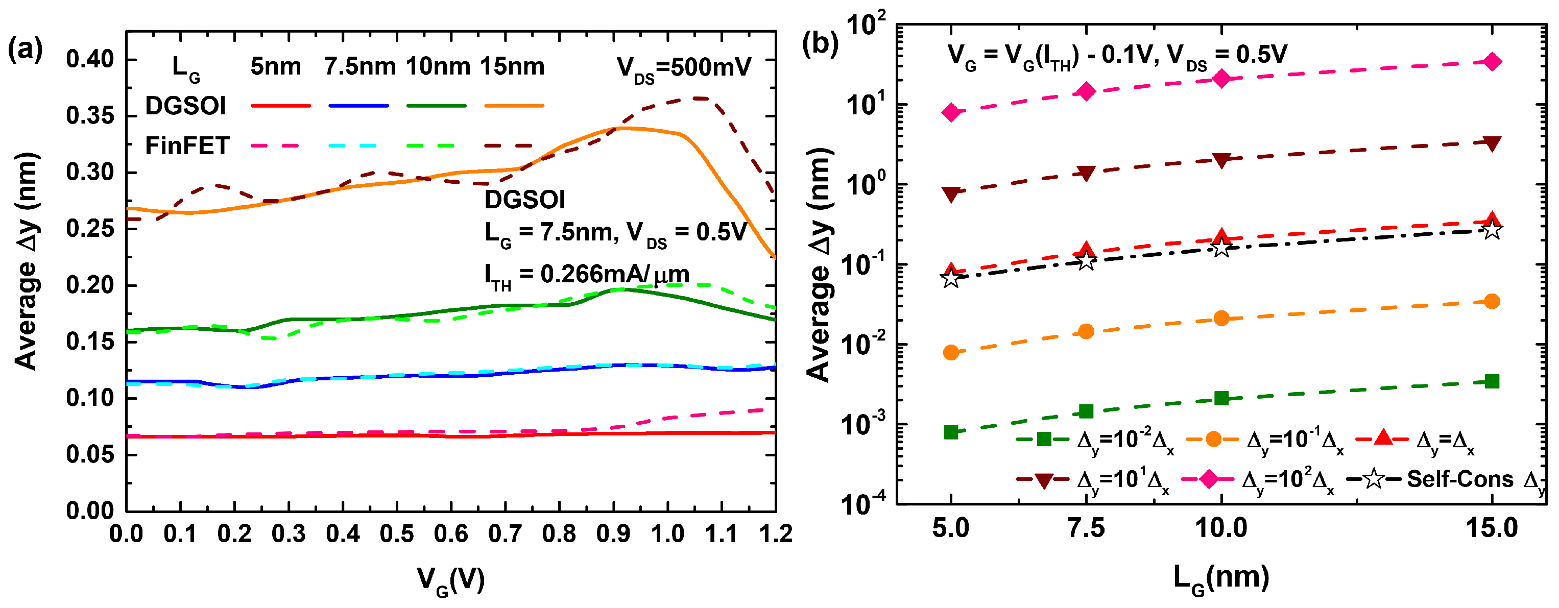
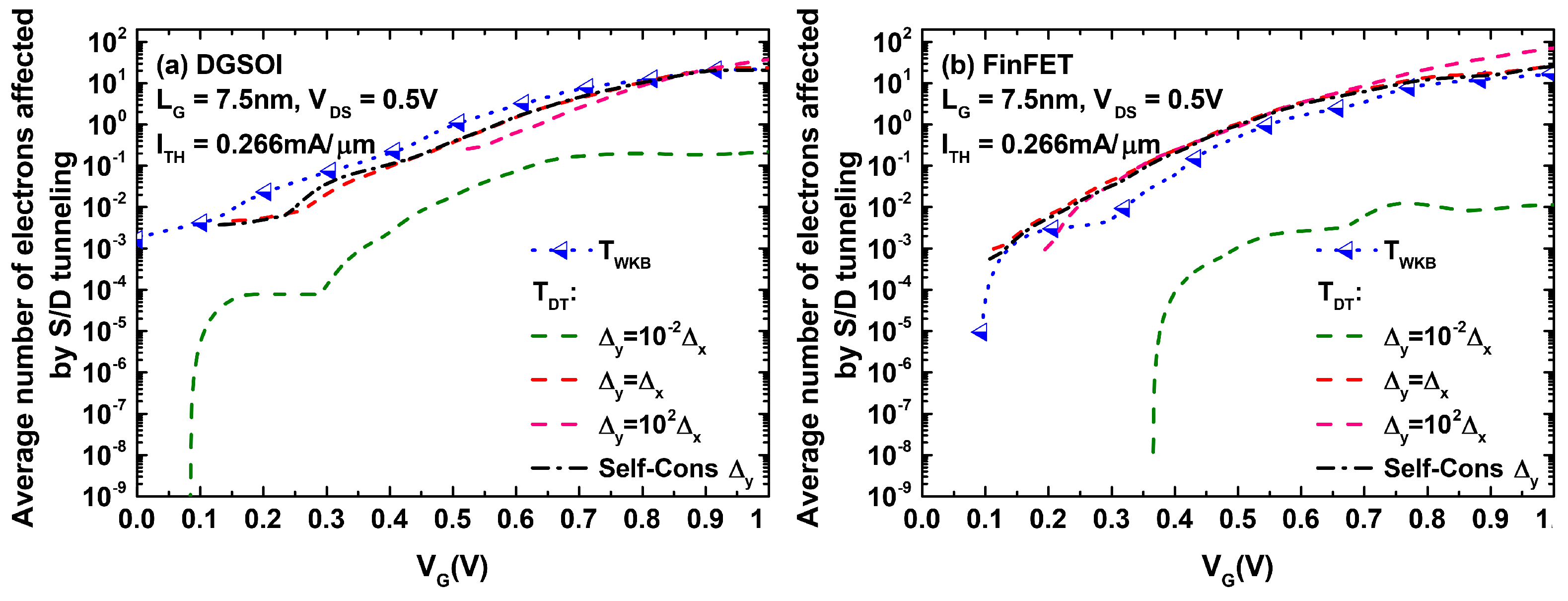
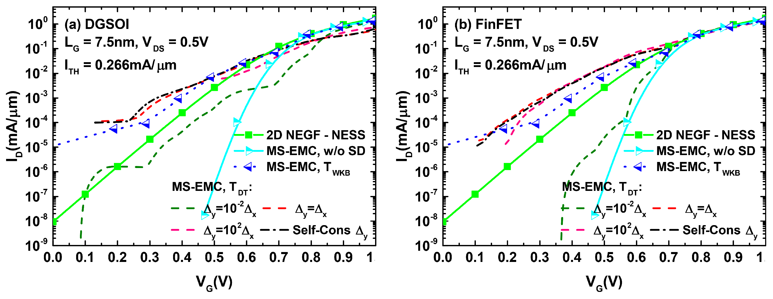
3.1. Comparison between the Different Implementations of the S/D Tunneling Probability in MS-EMC and the Simulation Results from NEGF
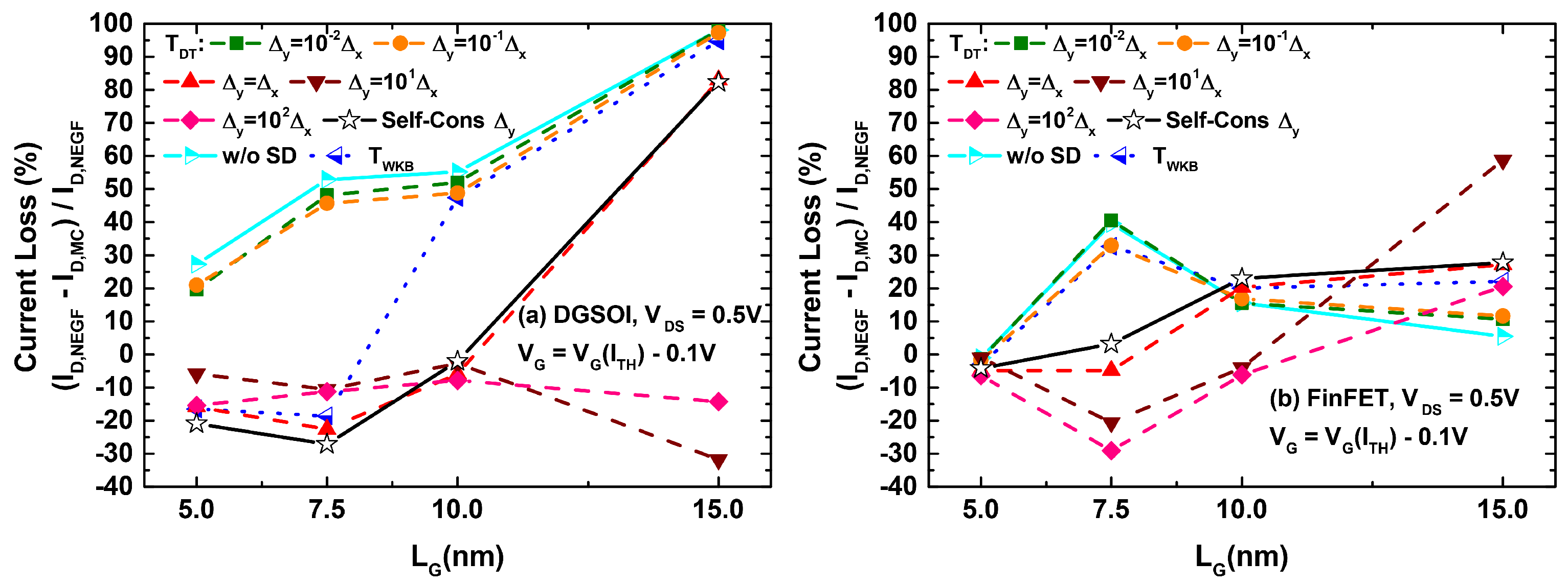
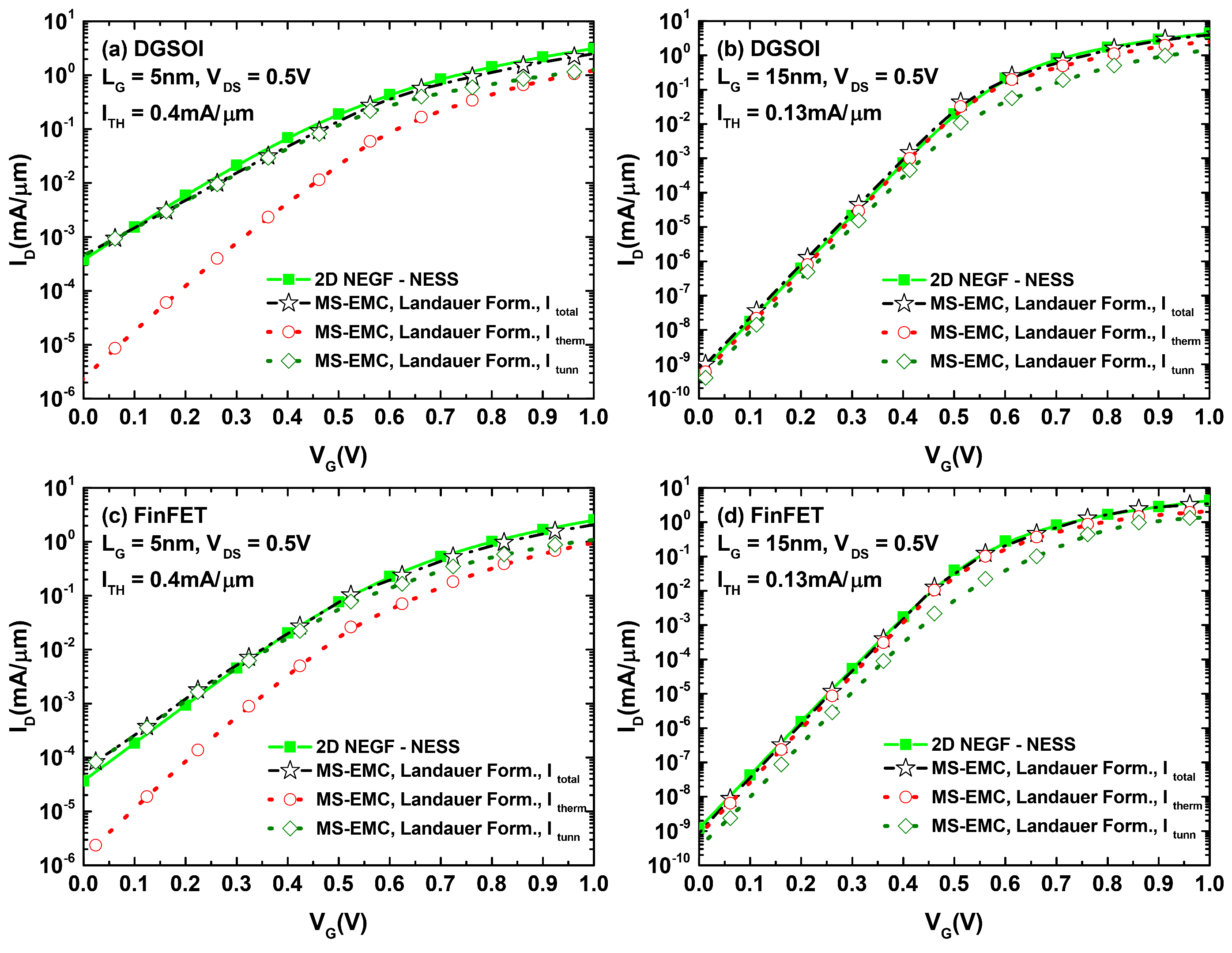
3.2. Comparison between the Different Current Computation Strategies in MS-EMC and the Simulation Results from NEGF
4. Conclusions
Author Contributions
Funding
Acknowledgments
Conflicts of Interest
References
- Medina-Bailon, C.; Padilla, J.; Sampedro, C.; Godoy, A.; Donetti, L.; Gámiz, F. Source–to–Drain Tunneling Analysis in FDSOI, DGSOI and FinFET Devices by Means of Multi-Subband Ensemble Monte Carlo. IEEE Trans. Electron Devices 2018, 65, 4740–4746. [Google Scholar] [CrossRef]
- Medina-Bailon, C.; Carrillo-Nunez, H.; Lee, J.; Sampedro, C.; Padilla, J.L.; Donetti, L.; Georgiev, V.; Gamiz, F.; Asenov, A. Quantum Enhancement of a S/D Tunneling Model in a 2D MS-EMC Nanodevice Simulator: NEGF Comparison and Impact of Effective Mass Variation. Micromachines 2020, 11, 204. [Google Scholar] [CrossRef]
- Wang, J.W.J.; Lundstrom, M. Does source-to-drain tunneling limit the ultimate scaling of MOSFETs? In Proceedings of the Digest. International Electron Devices Meeting, San Francisco, CA, USA, 8–11 December 2002; pp. 707–710. [Google Scholar] [CrossRef]
- Iwai, H. Future of nano CMOS technology. Solid-State Electron. 2015, 112, 56–67. [Google Scholar] [CrossRef]
- Berrada, S.; Dutta, T.; Carrillo-Nunez, H.; Duan, M.; Adamu-Lema, F.; Lee, J.; Georgiev, V.; Medina-Bailon, C.; Asenov, A. NESS: New flexible Nano-Electronic Simulation Software. In Proceedings of the 2018 International Conference on Simulation of Semiconductor Processes and Devices (SISPAD), Austin, TX, USA, 24–26 September 2018; pp. 22–25. [Google Scholar] [CrossRef]
- Berrada, S.; Carrillo-Nunez, H.; Lee, J.; Medina-Bailon, C.; Dutta, T.; Badami, O.; Adamu-Lema, F.; Thirunavukkarasu, V.; Georgiev, V.; Asenov, A. Nano-electronic Simulation Software (NESS): A flexible nano-device simulation platform. J. Comput. Electron. 2020, 19, 1031–1046. [Google Scholar] [CrossRef]
- Medina-Bailon, C.; Badami, O.; Carrillo-Nunez, H.; Dutta, T.; Nagy, D.; Adamu-Lema, F.; Georgiev, V.P.; Asenov, A. Enhanced Capabilities of the Nano-Electronic Simulation Software (NESS). In Proceedings of the 2020 International Conference on Simulation of Semiconductor Processes and Devices (SISPAD), Kobe, Japan, 23 September–6 October 2020; pp. 293–296. [Google Scholar] [CrossRef]
- Medina-Bailon, C.; Dutta, T.; Adamu-Lema, F.; Rezaei, A.; Nagy, D.; Gergiev, V.P.; Asenov, A. Nano-Electronic Simulation Software (NESS): A Novel Open-Source TCAD Simulation Environment. J. Microelectron. Manuf. Accept. Publ. 2020, 3, 20030407. [Google Scholar] [CrossRef]
- QuantumATK Version O-2018.06. [Synopsys, Inc., 2018]. 2018. Available online: https://www.synopsys.com/silicon/quantumatk// (accessed on 21 May 2021).
- Sampedro, C.; Donetti, L.; Gámiz, F.; Godoy, A. 3D Multi-Subband Ensemble Monte Carlo Simulator of FinFETs and Nanowire Transistors. In Proceedings of the 2014 International Conference on Simulation of Semiconductor Processes and Devices (SISPAD), Yokohama, Japan, 9–11 September 2014; pp. 21–24. [Google Scholar] [CrossRef]
- Sampedro, C.; Medina-Bailon, C.; Donetti, L.; Padilla, J.L.; Navarro, C.; Marquez, C.; Gamiz, F. Multi-Subband Ensemble Monte Carlo Simulator for Nanodevices in the End of the Roadmap. In Large-Scale Scientific Computations (LSSC); Springer International Publishing: Berlin, Germany, 2020; pp. 438–445. [Google Scholar] [CrossRef]
- Venugopal, R.; Ren, Z.; Datta, S.; Lundstrom, M.S.; Jovanovic, D. Simulating quantum transport in nanoscale transistors: Real versus mode-space approaches. J. Appl. Phys. 2002, 92, 3730–3739. [Google Scholar] [CrossRef]
- Medina-Bailon, C.; Padilla, J.; Sadi, T.; Sampedro, C.; Godoy, A.; Donetti, L.; Georgiev, V.; Gámiz, F.; Asenov, A. Multisubband Ensemble Monte Carlo Analysis of Tunneling Leakage Mechanisms in Ultrascaled FDSOI, DGSOI, and FinFET Devices. IEEE Trans. Electron Devices 2019, 66, 1145–1152. [Google Scholar] [CrossRef]
- Medina-Bailon, C.; Sampedro, C.; Padilla, J.L.; Godoy, A.; Donetti, L.; Gamiz, F.; Asenov, A. MS-EMC vs. NEGF: A comparative study accounting for transport quantum corrections. In Proceedings of the EUROSOI Workshop and International Conference on Ultimate Integration on Silicon (EUROSOI-ULIS), Granada, Spain, 19–21 March 2018; pp. 1–4. [Google Scholar] [CrossRef]
- Carrillo-Nunez, H.; Ziegler, A.; Luisier, M.; Schenk, A. Modeling direct band-to-band tunneling: From bulk to quantum-confined semiconductor devices. J. Appl. Phys. 2015, 117, 1234501. [Google Scholar] [CrossRef]
- Datta, S. Nanoscale device modelling: The Green’s function method. Superlattices Microstruct. 2000, 28, 253–278. [Google Scholar] [CrossRef]
- Luisier, M.; Schenk, A.; Fichtner, W. Quantum transport in two- and three-dimensional nanoscale transistors: Coupled mode effects in the nonequilibrium Greens function formalism. J. Appl. Phys. 2006, 100, 043713. [Google Scholar] [CrossRef]


Publisher’s Note: MDPI stays neutral with regard to jurisdictional claims in published maps and institutional affiliations. |
© 2021 by the authors. Licensee MDPI, Basel, Switzerland. This article is an open access article distributed under the terms and conditions of the Creative Commons Attribution (CC BY) license (https://creativecommons.org/licenses/by/4.0/).
Share and Cite
Medina-Bailon, C.; Padilla, J.L.; Sampedro, C.; Donetti, L.; Gergiev, V.P.; Gamiz, F.; Asenov, A. Self-Consistent Enhanced S/D Tunneling Implementation in a 2D MS-EMC Nanodevice Simulator. Micromachines 2021, 12, 601. https://doi.org/10.3390/mi12060601
Medina-Bailon C, Padilla JL, Sampedro C, Donetti L, Gergiev VP, Gamiz F, Asenov A. Self-Consistent Enhanced S/D Tunneling Implementation in a 2D MS-EMC Nanodevice Simulator. Micromachines. 2021; 12(6):601. https://doi.org/10.3390/mi12060601
Chicago/Turabian StyleMedina-Bailon, Cristina, José Luis Padilla, Carlos Sampedro, Luca Donetti, Vihar P. Gergiev, Francisco Gamiz, and Asen Asenov. 2021. "Self-Consistent Enhanced S/D Tunneling Implementation in a 2D MS-EMC Nanodevice Simulator" Micromachines 12, no. 6: 601. https://doi.org/10.3390/mi12060601
APA StyleMedina-Bailon, C., Padilla, J. L., Sampedro, C., Donetti, L., Gergiev, V. P., Gamiz, F., & Asenov, A. (2021). Self-Consistent Enhanced S/D Tunneling Implementation in a 2D MS-EMC Nanodevice Simulator. Micromachines, 12(6), 601. https://doi.org/10.3390/mi12060601