Article

Ionic-Liquid Gating in Two-Dimensional TMDs: The Operation Principles and Spectroscopic Capabilities

1
Nanotechnology Group, USAL–Nanolab, Universidad de Salamanca, E-37008 Salamanca, Spain
2
FIW Consulting S.L., Gabriel Garcia Marquez, 4 las Rozas, E-28232 Madrid, Spain
*
Authors to whom correspondence should be addressed.
Micromachines 2021, 12(12), 1576; https://doi.org/10.3390/mi12121576
Submission received: 15 November 2021 / Revised: 13 December 2021 / Accepted: 15 December 2021 / Published: 17 December 2021

Abstract

:
Ionic-liquid gating (ILG) is able to enhance carrier densities well above the achievable values in traditional field-effect transistors (FETs), revealing it to be a promising technique for exploring the electronic phases of materials in extreme doping regimes. Due to their chemical stability, transition metal dichalcogenides (TMDs) are ideal candidates to produce ionic-liquid-gated FETs. Furthermore, as recently discovered, ILG can be used to obtain the band gap of two-dimensional semiconductors directly from the simple transfer characteristics. In this work, we present an overview of the operation principles of ionic liquid gating in TMD-based transistors, establishing the importance of the reference voltage to obtain hysteresis-free transfer characteristics, and hence, precisely determine the band gap. We produced ILG-based bilayer WSe2 FETs and demonstrated their ambipolar behavior. We estimated the band gap directly from the transfer characteristics, demonstrating the potential of ILG as a spectroscopy technique.

1. Introduction

The discovery of two-dimensional materials unleashed a revolution in nanoelectronics during the last decade [1]. This family of materials holds enormous promise for the development of a new generation of semiconductor devices and, over the last few years, a considerable amount of effort has been invested in studying them and developing suitable devices that take advantage of their properties.
In 2011, Kis et al. demonstrated for the first time a field-effect transistor (FET) in which a bilayer MoS2 crystal was used as the semiconductor channel [2]. Since then, similar devices have been developed using several different two dimensional (2D) materials, and the device geometry, materials, and fabrication methods have been greatly improved [3].
However, FETs have certain fundamental limitations that cannot be easily overcome: the dielectric breakdown of the insulating layer and the presence of charged impurities between the gate electrode and the 2D channel results in a limited gating capability, which is often not sufficient to reach ambipolar response in 2D semiconductor devices. The technique of ionic-liquid gating (ILG) aims to overcome these fundamental limitations by replacing the dielectric material in conventional FETs with ionic liquids [4] with movable charged ions [5,6,7,8]. In recent years, ILG-based 2D transistors have been tested by a number of research groups, allowing them to achieve extremely large accumulations of charge carriers, up to 5 × 10¹⁴ electrons/cm2 while operating at moderate voltages within ±3 V [9].
Ionic-gating experiments have been widely used to control and investigate the electronic properties of oxides [7,10], nitrides [11], organic semiconductors [12,13,14], carbon-related materials [15], and III–V semiconductor nanowires [16,17,18,19]. The extreme tunability of charge carrier concentrations that can be obtained by this technique has allowed the attainment of new physical regimes, achieving, for example, superconductivity in band-insulating materials such as SrTiO3 (STO) [20], ZrNCl [11], or KTaO3 [21]. Currently, ILG has been established as a promising technique not only from an applied point of view, but also to obtain fundamental knowledge about the phase diagrams of novel materials [9,22]. More recently, ionic-gating experiments have moved forward through other inorganic systems, such as two-dimensional transition metal dichalcogenides (TMDs).
In this work, we present the operation principles for the use of ILG in TMD-based transistors. Due to their chemical stability, two-dimensional TMDs are ideal candidates to produce ionic liquid-gated FETs [23,24]. The very large geometrical capacitance of ionic liquid-gated devices allowed the observation of superconductivity in MoS2 [25,26,27,28,29,30,31] and WS2 [32,33,34], among other TMDs [35,36,37]. This technique has also enabled light emission by TMD-FETs operating in the ambipolar injection regime [38,39] and the enhancement of the electron−phonon interaction in multivalley TMDs [24,29,40]. Furthermore, as we present in this work, ILG-based TMD transistors grant the possibility of determining the band gap of semiconducting TMDs quantitatively from simple transport measurements [39,41,42,43,44].

2. Results

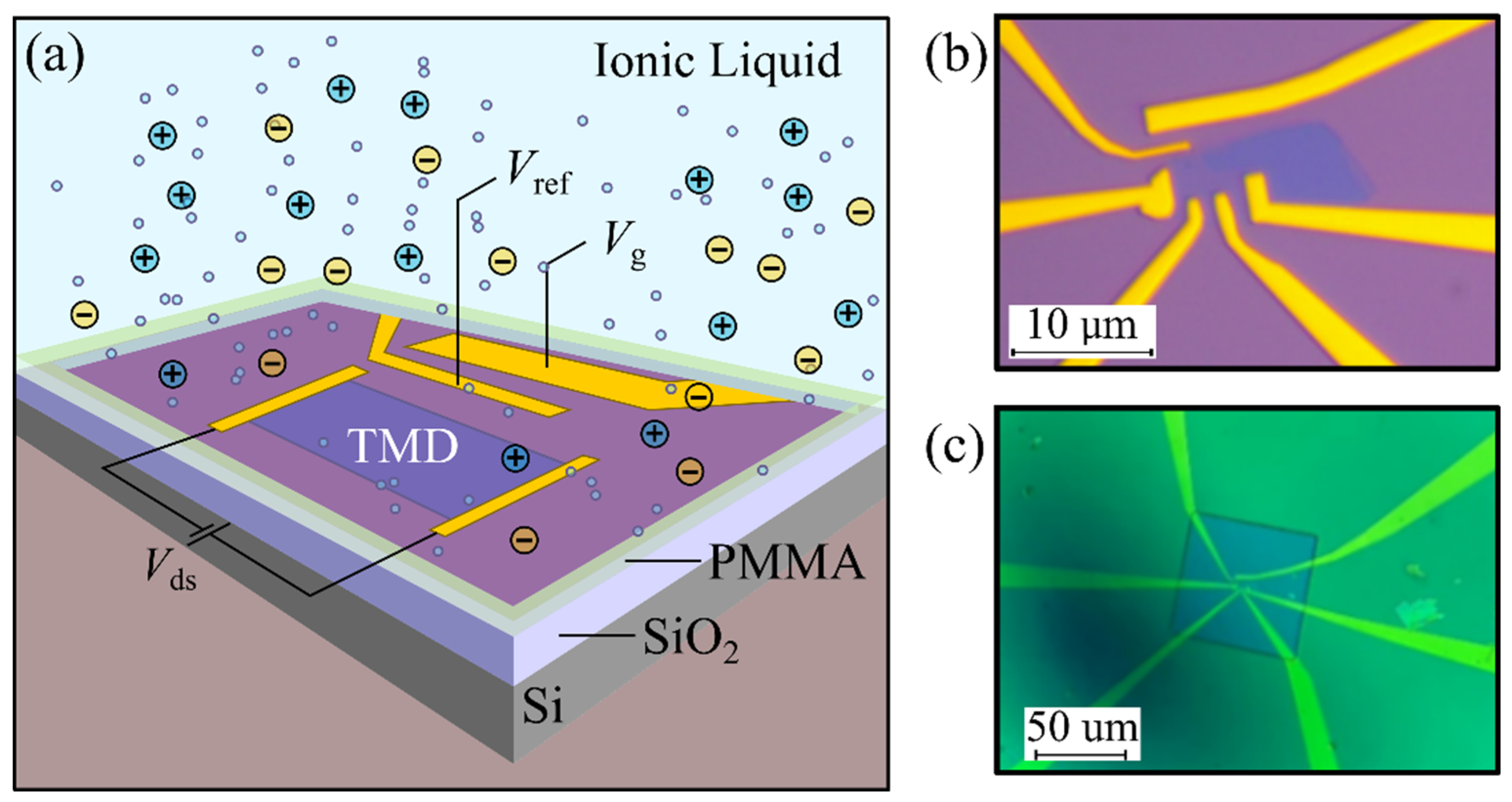
2.1. Device Fabrication and Geometry

Figure 1a schematically shows the geometry of a TMD-based ILG transistor. To illustrate the typical geometry and behavior of this family of transistors, we refer to the device shown in Figure 1b. In our case, the channel is a thin bilayer WSe2 crystal, fabricated by standard mechanical exfoliation and ulterior transfer onto a SiO2/Si substrate. The metallic electrodes were fabricated by e-beam lithography and evaporation of titanium and gold (5/45 nm). In addition to the four electrodes connected to the WSe2 flake, two electrodes were fabricated to act as the gate (Vg) and reference (Vref) electrodes. As a final step, the whole device was covered with a droplet of ionic liquid (DEME-TFSI), contacting the semiconductor channel, as well as the reference and gate electrodes (see Section S1 in Supplementary Materials for more information on the IL and its deposition). To minimize the exposure of the IL to the gold pads, the whole device was covered with polymethyl methacrylate (PMMA), leaving an exposed rectangular window on top of the semiconductor channel for placing the droplet (see Figure 1c).

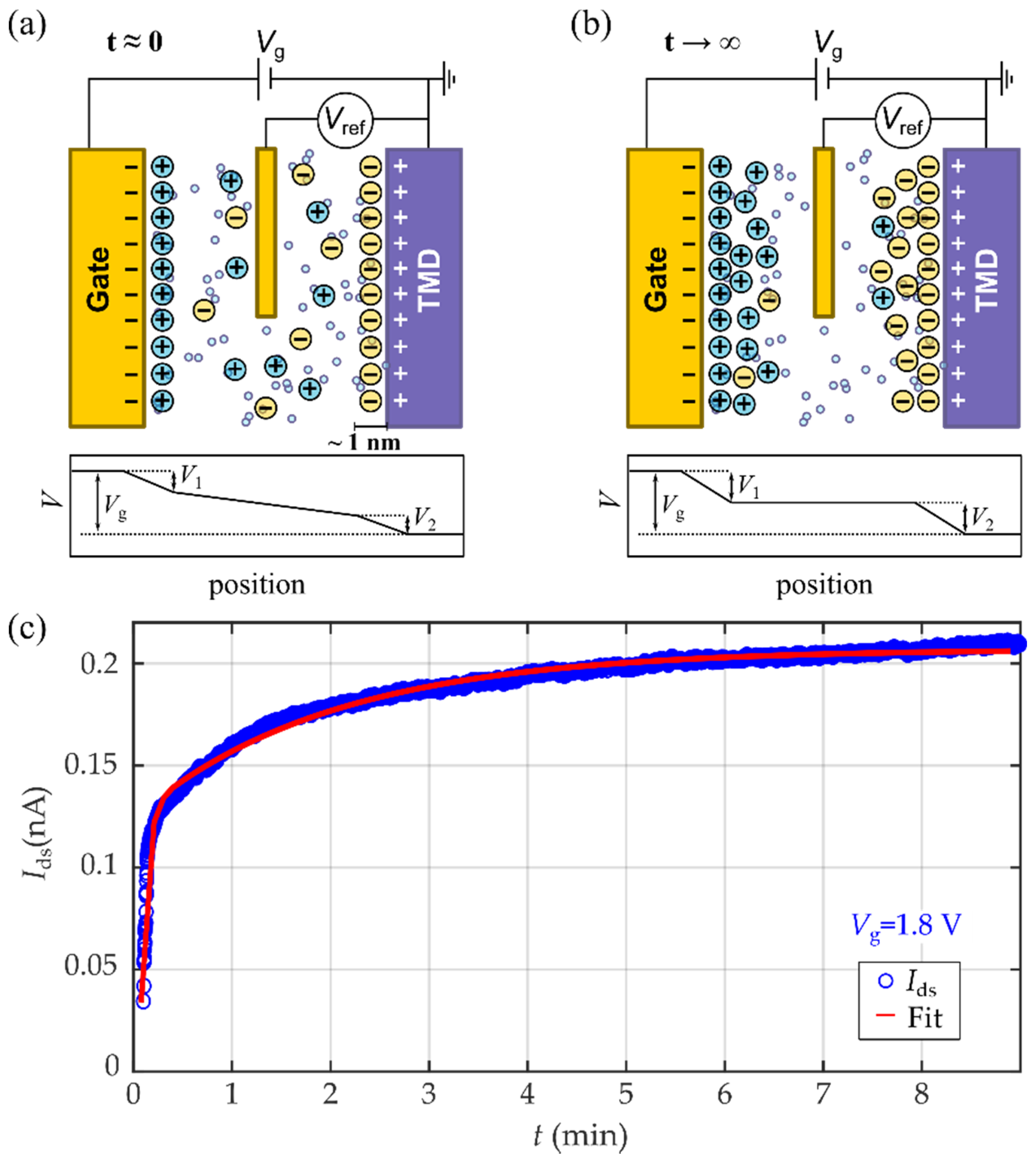
2.2. Basic Device Operation and Doping Mechanisms

The basic operation of the ILG transistor is depicted in Figure 2a,b. When a gate voltage is applied, the finite-sized ions accumulate in consecutive layers close to the TMD channel, forming a nanocapacitor that is typically 1 nm or less. It enhances a large electric field, resulting in a strong gating effect that can be controlled by the application of voltage to the gate electrode.
Figure 2c shows the time evolution of the drain-source current in the few-layer WSe2 IL-gated transistor, measured while switching the gate voltage from 0 to 1.8 V. The measured current I ds can be well-fitted to the equation for the charge process of two plane-parallel capacitors with different characteristic times:
I ds ( t ) = A + B ( 1 e t α 1 ) + C ( 1 e t α 2 )
where τ 1 , 2 = 1 α 1 , 2 are the characteristic times of the formation of the ionic layers that we use as fitting parameters. We obtained the characteristic times of τ 1 = 30   s and τ 2 = 23   min . These two characteristic times can be associated to the presence of two different charging processes. One is related to the fast formation of the first ion compact shells. The other one is caused by a slower migration and accumulation of ionic species in consecutive layers until the electric field inside the ionic liquid is fully screened [45].
While in early works, the doping effect in IL-gated FETs was attributed solely to the electrostatic screening of the accumulated charges at the interfaces, it is now clear that two main mechanisms govern ionic-liquid gating, depending on the characteristics of both the electrolyte and the material used as a channel [46]: electrostatic doping (described above) and electrochemical doping. For this second mechanism, the migration of ions within the material plays a key role and may induce an irreversible behavior caused by chemical degradation. Electrochemical doping is often the dominant gating mechanism when the IL is used in combination with transition metal oxides. In this case, the doping process also involves the migration of oxygen atoms from the crystallographic unit cell. The oxygen atoms act as dopants, enabling the introduction of charge carriers into the system [47,48,49]. However, in the case of semiconducting TMDs, ionic gating has an almost pure electrostatic effect and does not cause any chemical modification, as long as the applied gate voltage is kept within a suitable range, which results in stable and reversible transistor operation.

2.3. The Need for a Reference Electrode

In a conventional metal–oxide–semiconductor field-effect transistor (MOSFET), the applied gate voltage, Vg, uniformly drops across the gate dielectric. However, as depicted in Figure 2a,b and discussed above, in EDL transistors the voltage drop concentrates in the neighboring regions of the gate electrode (V1) and the channel (V2). Thus, in equilibrium we have:
V g = V 1 + V 2 ,
and only a portion of V2 of the applied voltage, Vg, contributes to gating.
In the hypothetical situation in which V1 becomes negligible, the applied gate voltage, Vg, drops entirely at the IL/WSe2 interface (V2 = ΔVg). Experimentally, in ILG measurements, the gate electrode is usually (and intentionally) fabricated to have a large surface area, so the contribution of V1 can be minimal; however, it cannot be neglected.
In general, V1 and V2 do not change linearly with Vg, and, furthermore, they may fluctuate over time and/or present hysteretic behaviors. In consequence, it is necessary to introduce a reference electrode, Vref, to monitor V2 situated in contact with the ionic liquid (see Figure 2a,b). For sufficiently long times, once the EDLs are fully formed, Vref will be given by:
V ref = V g V 1 = V 2 .
Thus, Vref provides us with a direct measurement of the voltage drop at the liquid/TMD interface, which is responsible for the gating effect.

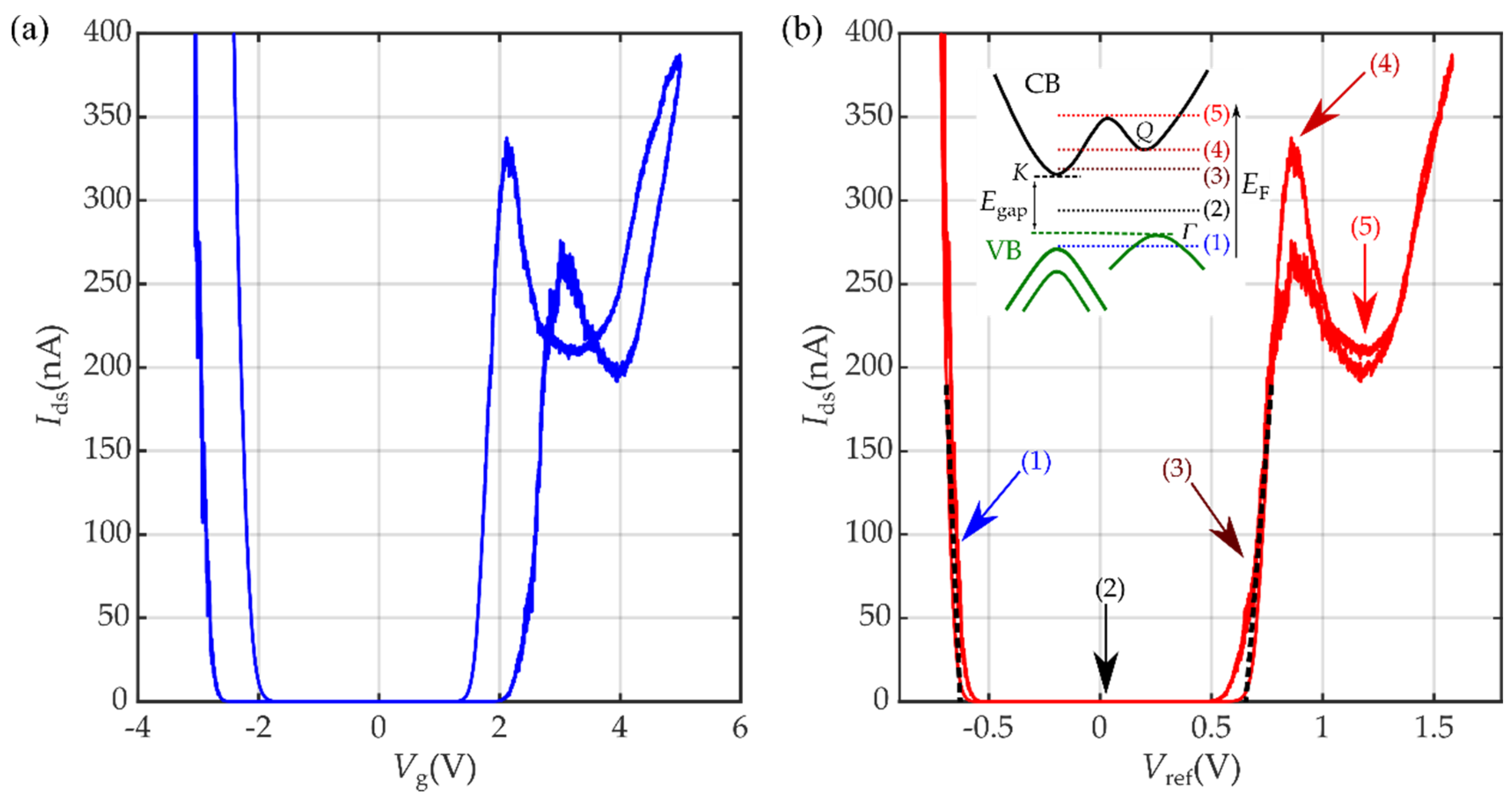
2.4. Nonmonotonic Behavior in Transfer Characteristics and Estimation of Semiconductor Band Gap

Figure 3 shows the transfer characteristic of a WSe2 ILG transistor, measured at 240 K (see Section S2 for measurements at other temperatures). As mentioned in the previous section, when the drain-source current is plotted against the gate voltage, VG (Figure 3a), a large hysteresis appears because of the slow process of ion diffusion in the ionic liquid. However, this hysteresis largely decreases when Ids is represented as a function of Vref (Figure 3b).
The large shifts in the Fermi energy that can be achieved in ILG transistors allow us to observe ambipolar conduction in the transfer characteristic even while applying moderate gate voltages. A large source-drain current, Ids, is measured for both high negative and positive Vg. When the Fermi level is in the WSe2 band gap (OFF state), the measured current is just 10 pA, indicating there is almost no hopping conductivity because of intragap states or unintentional dopants in the material [41] and confirming the high quality of the WSe2 flake.
For positive gate voltages (Vg > 0), the transfer curve shows a nonmonotonic behavior, also described in the literature using different ionic liquids [50]. This has been found to be related to a nonlinearity that is present in the electron density because of intervalley scattering processes. This intervalley scattering becomes possible when the chemical potential is shifted into a higher energy valley. WSe2 bilayers exhibit an indirect band gap between the conduction band minimum at Γ and the valence band maximum at K in the first Brillouin zone (BZ) [51]. Upon adding electrons, the K valley is filled first to above a certain value (denoted by (4) in the inset of Figure 3b), and the Q valley also starts to be filled. This inflection point enabled the quantitative determination of the energy difference between the K and Q valleys of monolayer WSe2 in the literature, E Q E K = 108   meV [50]. We estimated the energy difference between the K and Q valleys for bilayer WSe2, E Q E K = 40 meV (see Section S3), to be in agreement with the value obtained in the literature [51]. For negative gate voltages (Vg < 0), this nonmonotonic behavior is not observed. In this case, the second valley to be depleted of electrons would be the valley centered at K. However, the required hole density to reach this second valley is above the values achieved in our measurements.

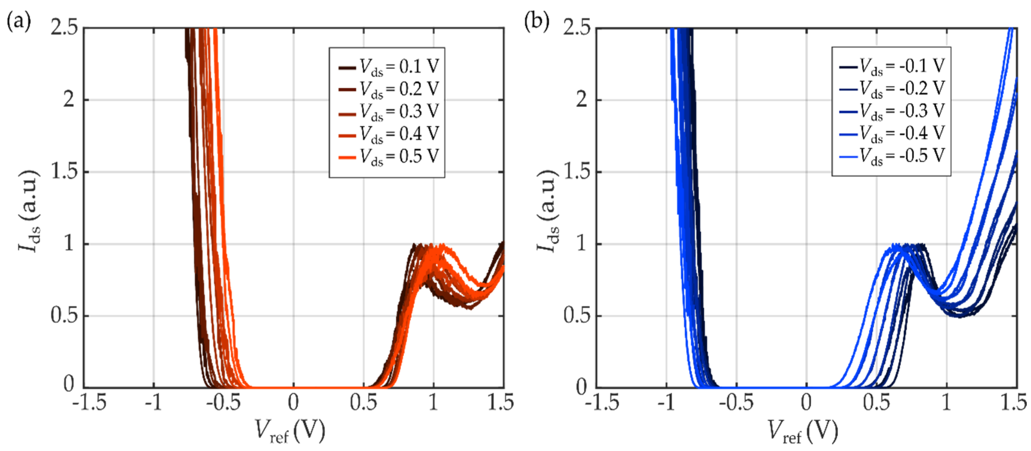
2.5. ILG: A Spectroscopy Technique to Estimate the Semiconductor Band Gap

Currently, determining the band gap of two-dimensional semiconductors is usually undertaken using optical techniques [52,53,54] or by scanning tunneling spectroscopy (STS) [55,56], although complex techniques, such as angle-resolved photoemission spectroscopy (ARPES) [57,58], have also been used. However, these first two commonly used techniques require modeling of the measured data to extract a quantitative value for the gap. In optical techniques, an analysis of excited exciton states is required, this being a hard approach for indirect band gap semiconductors. In the case of the STS, the measured differential conductance must be modeled because the tip acts as a local gate, shifting the energy of the band edge and modifying the probability of electrons tunneling through vacuum.
As recently proved by Morpurgo et al. [53], IL gating can be used as a spectroscopy technique to precisely determine the band gap of a semiconductor from simple transport measurements. Because of the close proximity of the ionic liquid to the semiconductor channel, donor or acceptor impurities are negligible at the interface. Thus, a change in the gate voltage (or more precisely in the reference potential, ΔVref) is directly related to a shift in chemical potential, and the difference between V th e and V th h is a direct measurement of the semiconductor band gap.
A change in reference voltage induces a change in both the chemical potential, Δ μ , and the electrostatic potential, Δ φ :
e Δ V ref   =   Δ μ + e Δ φ .
The electrostatic potential in a parallel-plate capacitor can be defined as:
Δ φ = e Δ n C G ,
where Δn is the density of accumulated charge carriers at the capacitor plate and C G is the geometric capacitance.
For Fermi energies within the TMD band gap, Δn is small because, ideally, there are no available states to be occupied by charge carriers, and the term Δφ in Equation (4) can be disregarded. In this situation, a shift in gate voltage induces an identical shift in chemical potential:
e Δ V ref = Δ μ .
Therefore, the band gap of the semiconductor channel, E gap , can then be determined as:
E g a p = e   ( V th e V th h ) ,
since V th e and V th h correspond to having μ located, respectively, at the conduction and valence band edges.
Figure 4 shows the transfer characteristics of the WSe2 device measured at different positive (Figure 4a) and negative (Figure 4b) drain-source voltages, Vds. The threshold voltage values for electrons, V th e , and holes, V th h , were obtained by linearly extrapolating to zero the I ds V ref characteristics, (see black dashed lines in Figure 3b). To perform the extrapolation properly, it is important to identify a sufficiently large range of Vref in the linear regime, out of the sub-threshold region, in which Ids increases exponentially on Vref [59].
The band gap is estimated by extrapolating to V ds = 0   V . We obtain:
E WSe 2 = e   ( V th e V th h ) = 1.3   eV ,
with an ∼±5% experimental error that originated from the extrapolation procedure. This value agrees with the band gap measured with experimental techniques (1.5−1.6 eV) [51,59,60,61,62], as well as with the value estimated theoretically for bilayer WSe2 (1.1 eV) [45]. At high Vds, linear shifts in the threshold voltage appear. This threshold voltage was previously associated in WS2 with uncertainties in the measurements [41] and here we relate it to the position dependence of the reference electrode, its geometry and area indicating the need to measure with low Vds because of the strong dependence on the localization of the reference electrode. The leakage current was also measured during the experiment, keeping the values below 0.05 nA (see Section S4 for more information).

3. Conclusions

In this work, we described and demonstrated the operation principles of ionic liquid gating in TMD-based transistors. We produced an ambipolar field-effect transistor with bilayer WSe2 flake crystals, explaining the importance of the reference voltage, Vref, for obtaining hysteresis-free transfer characteristics. ILG allowed us to obtain steep subthreshold slopes for both electrons and holes and extremely low OFF-state currents. We obtained evidence of the potential spectroscopic capabilities of ionic-liquid-gated transistors by acquiring the band gap of bilayer WSe2 directly from those measurements.
The possibility of quantitatively determining the band gaps and band offsets directly from simple transfer characteristics makes the IL gating a promising new technique, ideal for characterizing 2D semiconductor materials and their heterostructures.

Supplementary Materials

Supplementary material is available online at https://www.mdpi.com/article/10.3390/mi12121576/s1, S1: Deposition of the ionic liquid DEME-TFSI, S2: Transfer curves at different temperatures, Figure S1: Transfer characteristics of the bilayer WSe2 ionic liquid-gated transistor, S3: Estimation of the energy splitting between valleys Q-K in bilayer WSe2, S4: Measuring the gate leakage current and the linear dependence of Vref and Vgate, Figure S2 Gate leakage current, IG, measured between the gate electrode and the device as function of the reference voltage, Vref while sweeping the gate voltage, Vg, at 1 mV/s.

Author Contributions

E.D. and A.M.P.-M. conceived and supervised the research; V.C., J.S.-S. and A.M.P.-M. fabricated the devices; D.V., J.Q. and A.M.P.-M. carried out the experimental measurements and data analysis. The article was written with contributions from all the authors, coordinated by A.M.P.-M. All authors have read and agreed to the published version of the manuscript.

Funding

This research was funded by Agencia Estatal de Investigación of Spain (Grant PID2019-106820RB) and the Junta de Castilla y León (Grants SA256P18 and SA121P20), including funding by ERDF/FEDER. J.Q. acknowledges financial support from MICINN (Spain) through the Juan de la Cierva-Incorporación program. A.M.P.-M. acknowledges financial support from the Spanish Ministry of Science and Innovation under the Torres Quevedo grant, TQ2019-010689/AEI/10.13039/501100011033. D.V. acknowledges financial support from the Ministerio de Universidades (Spain) (Ph.D. contract FPU19/04224), including funding from ERDF/FEDER. J.S. acknowledges financial support for his Ph.D. contract from the Consejería de Educación, Junta de Castilla y Leon, and ERDF/FEDER.

Data Availability Statement

The data that support the findings of this study are available from the corresponding author upon reasonable request.

Acknowledgments

We thank Adrián Martín for his help during sample fabrication and the Research Group on High-Frequency Nanoelectronic Devices of USAL-NANOLAB for the use a low-temperature probe station during the experimental measurements.

Conflicts of Interest

The authors declare no conflict of interest.

References

  1. Novoselov, K.S.; Mishchenko, A.; Carvalho, A.; Castro Neto, A.H. 2D Materials and van Der Waals Heterostructures. Science 2016, 353, aac9439. [Google Scholar] [CrossRef] [Green Version]
  2. Radisavljevic, B.; Radenovic, A.; Brivio, J.; Giacometti, V.; Kis, A. Single-Layer MoS2 Transistors. Nat. Nano 2011, 6, 147–150. [Google Scholar] [CrossRef]
  3. Liu, Y.; Duan, X.; Shin, H.J.; Park, S.; Huang, Y.; Duan, X. Promises and Prospects of Two-Dimensional Transistors. Nature 2021, 591, 43–53. [Google Scholar] [CrossRef] [PubMed]
  4. Brattain, B.W.H.; Garrett, C.G.B. Experiments on the Interface Hetween Germanium and an Electrolyte. Bell Syst. Tech. J. 1954, 34, 129–176. [Google Scholar] [CrossRef]
  5. Shimotani, H.; Asanuma, H.; Takeya, J.; Iwasa, Y. Electrolyte-Gated Charge Accumulation in Organic Single Crystals. Appl. Phys. Lett. 2006, 89, 203501. [Google Scholar] [CrossRef]
  6. Shimotani, H.; Asanuma, H.; Tsukazaki, A.; Ohtomo, A.; Kawasaki, M.; Iwasa, Y. Insulator-to-Metal Transition in ZnO by Electric Double Layer Gating. Appl. Phys. Lett. 2007, 91, 15–18. [Google Scholar] [CrossRef]
  7. Yuan, H.; Shimotani, H.; Tsukazaki, A.; Ohtomo, A.; Kawasaki, M.; Iwasa, Y. High-Density Carrier Accumulation in ZnO Field-Effect Transistors Gated by Electric Double Layers of Ionic Liquids. Adv. Funct. Mater. 2009, 19, 1046–1053. [Google Scholar] [CrossRef]
  8. Yuan, H.; Shimotani, H.; Tsukazaki, A.; Ohtomo, A. Hydrogenation-Induced Surface Polarity Recognition and Proton Memory Behavior at Protic-Ionic-Liquid/Oxide Electric-Double-Layer Interfaces. J. Am. Chem. Soc. 2010, 132, 6672–6678. [Google Scholar] [CrossRef]
  9. Bisri, S.Z.; Shimizu, S.; Nakano, M.; Iwasa, Y. Endeavor of Iontronics: From Fundamentals to Applications of Ion-Controlled Electronics. Adv. Mater. 2017, 29, 1607054. [Google Scholar] [CrossRef]
  10. Yamada, Y.; Ueno, K.; Fukumura, T.; Yuan, H.T.; Shimotani, H.; Iwasa, Y.; Gu, L.; Tsukimoto, S.; Ikuhara, Y.; Kawasaki, M. Electrically Induced Ferromagnetism at Room Temperature in Cobalt-Doped Titanium Dioxide. Science 2011, 332, 1065–1067. [Google Scholar] [CrossRef]
  11. Ye, J.T.; Inoue, S.; Kobayashi, K.; Kasahara, Y.; Yuan, H.T.; Shimotani, H.; Iwasa, Y. Liquid-Gated Interface Superconductivity on an Atomically Flat Film. Nat. Mater. 2010, 9, 125–128. [Google Scholar] [CrossRef]
  12. Kim, S.H.; Hong, K.; Xie, W.; Lee, K.H.; Zhang, S.; Lodge, T.P.; Frisbie, C.D. Electrolyte-Gated Transistors for Organic and Printed Electronics. Adv. Mater. 2013, 25, 1822–1846. [Google Scholar] [CrossRef] [PubMed]
  13. Xia, B.Y.; Cho, J.H.; Lee, J.; Ruden, P.P.; Frisbie, C.D. Comparison of the Mobility–Carrier Density Relation in Polymer and Single-Crystal Organic Transistors Employing Vacuum and Liquid Gate Dielectrics. Adv. Mater. 2009, 21, 2174–2179. [Google Scholar] [CrossRef]
  14. Leger, J.; Berggren, M.; Carter, S.; Berggren, M.; Carter, S. Iontronics: Ionic Carriers in Organic Electronic Materials and Devices; CRC Press: Boca Raton, FL, USA, 2016. [Google Scholar]
  15. You, A.; Be, M.A.Y.; In, I. Electrochemical Carbon Nanotube Field-Effect Transistor. Appl. Phys. Lett. 2007, 78, 1291. [Google Scholar] [CrossRef] [Green Version]
  16. Lieb, J.; Demontis, V.; Prete, D.; Ercolani, D.; Zannier, V.; Sorba, L.; Ono, S.; Beltram, F.; Sacépé, B.; Rossella, F. Ionic-Liquid Gating of InAs Nanowire-Based Field-Effect Transistors. Adv. Funct. Mater. 2019, 29, 1804378. [Google Scholar] [CrossRef] [Green Version]
  17. Demontis, V.; Zannier, V.; Sorba, L.; Rossella, F. Surface Nano-Patterning for the Bottom-Up Growth of III-V Semiconductor Nanowire Ordered Arrays. Nanomaterials 2021, 11, 2079. [Google Scholar] [CrossRef]
  18. Ullah, A.R.; Carrad, D.J.; Krogstrup, P.; Nygård, J.; Micolich, A.P. Near-Thermal Limit Gating in Heavily Doped III-V Semiconductor Nanowires Using Polymer Electrolytes. Phys. Rev. Mater. 2018, 2, 25601. [Google Scholar] [CrossRef] [Green Version]
  19. Carrad, D.J.; Mostert, A.B.; Ullah, A.R.; Burke, A.M.; Joyce, H.J.; Tan, H.H.; Jagadish, C.; Krogstrup, P.; Nygård, J.; Meredith, P. Hybrid Nanowire Ion-to-Electron Transducers for Integrated Bioelectronic Circuitry. Nano Lett. 2017, 17, 827–833. [Google Scholar] [CrossRef] [Green Version]
  20. Ueno, K.; Nakamura, S.; Shimotani, H.; Ohtomo, A.; Kimura, N.; Nojima, T.; Aoki, H.; Iwasa, Y.; Kawasaki, M. Electric-Field-Induced Superconductivity in an Insulator. Nat. Mater. 2008, 7, 855–858. [Google Scholar] [CrossRef]
  21. Ueno, K.; Nakamura, S.; Shimotani, H.; Yuan, H.T.; Kimura, N.; Nojima, T.; Aoki, H.; Iwasa, Y.; Kawasaki, M. Discovery of Superconductivity in KTaO3 by Electrostatic Carrier Doping. Nat. Nanotechnol. 2011, 6, 408–412. [Google Scholar] [CrossRef] [PubMed]
  22. Fujimoto, T.; Awaga, K. Electric-Double-Layer Field-Effect Transistors with Ionic Liquids. Phys. Chem. Chem. Phys 2013, 15, 8983–9006. [Google Scholar] [CrossRef] [PubMed]
  23. Yuan, H.T.; Toh, M.; Morimoto, K.; Tan, W.; Wei, F.; Shimotani, H.; Kloc, C.; Iwasa, Y. Liquid-Gated Electric-Double-Layer Transistor on Layered Metal Dichalcogenide, SnS2. Appl. Phys. Lett. 2011, 98, 012102. [Google Scholar] [CrossRef]
  24. Zhang, Y.; Ye, J.; Matsuhashi, Y.; Iwasa, Y. Ambipolar MoS2 Thin Flake Transistors. Nano Lett. 2012, 12, 1136–1140. [Google Scholar] [CrossRef]
  25. Ye, J.T.; Zhang, Y.J.; Akashi, R.; Bahramy, M.S.; Arita, R.; Iwasa, Y. Superconducting Dome in a Gate-Tuned Band Insulator. Science 2012, 338, 1193–1196. [Google Scholar] [CrossRef] [PubMed]
  26. Biscaras, J.; Chen, Z.; Paradisi, A.; Shukla, A. Onset of Two-Dimensional Superconductivity in Space Charge Doped Few-Layer Molybdenum Disulfide. Nat. Commun. 2015, 6, 8826. [Google Scholar] [CrossRef] [Green Version]
  27. Costanzo, D.; Jo, S.; Berger, H.; Morpurgo, A.F. Gate-Induced Superconductivity in Atomically Thin MoS2 Crystals. Nat. Nanotechnol. 2016, 11, 339–344. [Google Scholar] [CrossRef] [Green Version]
  28. Costanzo, D.; Zhang, H.; Reddy, B.A.; Berger, H.; Morpurgo, A.F. Tunnelling Spectroscopy of Gate-Induced Superconductivity in MoS2. Nat. Nanotechnol. 2018, 13, 483–488. [Google Scholar] [CrossRef] [Green Version]
  29. Piatti, E.; De Fazio, D.; Daghero, D.; Tamalampudi, S.R.; Yoon, D.; Ferrari, A.C.; Gonnelli, R.S. Multi-Valley Superconductivity in Ion-Gated MoS2 Layers. Nano Lett. 2018, 18, 4821–4830. [Google Scholar] [CrossRef] [Green Version]
  30. Lu, J.M.; Zheliuk, O.; Leermakers, I.; Yuan, N.F.Q.; Zeitler, U.; Law, K.T.; Ye, J.T. Evidence for Two-Dimensional Ising Superconductivity in Gated MoS2. Science 2015, 350, 1353–1358. [Google Scholar] [CrossRef] [Green Version]
  31. Saito, Y.; Nakamura, Y.; Bahramy, M.S.; Kohama, Y.; Ye, J.; Kasahara, Y.; Nakagawa, Y.; Onga, M.; Tokunaga, M.; Nojima, T.; et al. Superconductivity Protected by Spin-Valley Locking in Ion-Gated MoS2. Nat. Phys. 2016, 12, 144–149. [Google Scholar] [CrossRef]
  32. Dhoot, A.S.; Israel, C.; Moya, X.; Mathur, N.D.; Friend, R.H. Large Electric Field Effect in Electrolyte-Gated Manganites. Phys. Rev. Lett. 2009, 102, 136402. [Google Scholar] [CrossRef]
  33. Jo, S.; Costanzo, D.; Berger, H.; Morpurgo, A.F. Electrostatically Induced Superconductivity at the Surface of WS2. Nano Lett. 2015, 15, 1197–1202. [Google Scholar] [CrossRef] [PubMed] [Green Version]
  34. Lu, J.; Zheliuk, O.; Chen, Q.; Leermakers, I.; Hussey, N.E.; Zeitler, U.; Ye, J. Full Superconducting Dome of Strong Ising Protection in Gated Monolayer WS2. Proc. Natl. Acad. Sci. USA 2018, 115, 3551–3556. [Google Scholar] [CrossRef] [PubMed] [Green Version]
  35. Shi, W.; Ye, J.; Zhang, Y.; Suzuki, R.; Yoshida, M.; Miyazaki, J.; Inoue, N.; Saito, Y.; Iwasa, Y. Superconductivity Series in Transition Metal Dichalcogenides by Ionic Gating. Sci. Rep. 2015, 5, 12534. [Google Scholar] [CrossRef] [PubMed] [Green Version]
  36. Kouno, S.; Sato, Y.; Katayama, Y.; Ichinose, A.; Asami, D. Superconductivity at 38 K at an Electrochemical Interface between Various Substrates. Sci. Rep. 2018, 8, 14731. [Google Scholar] [CrossRef]
  37. Zeng, J.; Liu, E.; Fu, Y.; Chen, Z.; Pan, C.; Wang, C.; Wang, M.; Wang, Y.; Xu, K.; Cai, S.; et al. Gate-Induced Interfacial Superconductivity in 1T-SnSe2. Nano Lett. 2018, 18, 1410–1415. [Google Scholar] [CrossRef] [Green Version]
  38. Zhang, Y.J.; Oka, T.; Suzuki, R.; Ye, J.T.; Iwasa, Y. Electrically Switchable Chiral Light-Emitting Transistor. Science 2014, 344, 725–728. [Google Scholar] [CrossRef]
  39. Jo, S.; Ubrig, N.; Berger, H.; Kuzmenko, A.B.; Morpurgo, A.F. Mono- and Bilayer WS2 Light-Emitting Transistors. Nano Lett. 2014, 14, 2019–2025. [Google Scholar] [CrossRef] [Green Version]
  40. Sohier, T.; Ponomarev, E.; Gibertini, M.; Berger, H.; Marzari, N.; Ubrig, N.; Morpurgo, A.F. Enhanced Electron-Phonon Interaction in Multivalley Materials. Phys. Rev. X 2019, 9, 31019. [Google Scholar] [CrossRef] [Green Version]
  41. Braga, D.; Gutiérrez Lezama, I.; Berger, H.; Morpurgo, A.F. Quantitative Determination of the Band Gap of WS2 with Ambipolar Ionic Liquid-Gated Transistors. Nano Lett. 2012, 12, 5218–5223. [Google Scholar] [CrossRef] [Green Version]
  42. Lezama, I.G.; Ubaldini, A.; Longobardi, M.; Giannini, E.; Renner, C.; Kuzmenko, A.B.; Morpurgo, A.F. Surface Transport and Band Gap Structure of Exfoliated. 2D Mater. 2014, 1, 021002. [Google Scholar] [CrossRef] [Green Version]
  43. Berger, H.; Ponomarev, E.; Ubrig, N.; Gutie, I.; Morpurgo, A.F. Semiconducting van Der Waals Interfaces as Arti Fi Cial Semiconductors. Nano Lett. 2018, 18, 5146–5152. [Google Scholar] [CrossRef]
  44. Waelchli, A.; Scarfato, A.; Ubrig, N.; Renner, C.; Morpurgo, A.F. Hole Transport in Exfoliated Monolayer MoS2. ACS Nano 2018, 12, 2669–2676. [Google Scholar] [CrossRef] [Green Version]
  45. Oldham, K.B. A Gouy-Chapman-Stern Model of the Double Layer at a (Metal)/(Ionic Liquid) Interface. J. Electroanal. Chem. 2008, 613, 131–138. [Google Scholar] [CrossRef]
  46. Lee, J.; Kaake, L.G.; Cho, J.H.; Zhu, X.; Lodge, T.P.; Frisbie, C.D. Ion Gel-Gated Polymer Thin-Film Transistors: Operating Mechanism and Characterization of Gate Dielectric Capacitance, Switching Speed, and Stability. J. Phys. Chem. C 2009, 113, 8972–8981. [Google Scholar] [CrossRef]
  47. Li, M.; Han, W.; Jiang, X.; Jeong, J.; Samant, M.G.; Parkin, S.S.P. Suppression of Ionic Liquid Gate-Induced Metallization of SrTiO3(001) by Oxygen. Nano Lett. 2013, 13, 4675–4678. [Google Scholar] [CrossRef] [PubMed]
  48. Jeong, J.; Aetukuri, N.; Graf, T.; Schladt, T.D.; Samant, M.G.; Parkin, S.S.P. Suppression of Metal-Insulator Transition in VO2 by Electric Field-Induced Oxygen Vacancy Formation. Science 2013, 339, 1402–1405. [Google Scholar] [CrossRef] [PubMed]
  49. Perez-Muñoz, A.M.; Schio, P.; Poloni, R.; Fernandez-Martinez, A.; Rivera-Calzada, A.; Cezar, J.C.; Salas-Colera, E.; Castro, G.R.; Kinney, J.; Leon, C.; et al. In Operando Evidence of Deoxygenation in Ionic Liquid Gating of YBa2Cu3O7-X. Proc. Natl. Acad. Sci. USA 2017, 114, 215–220. [Google Scholar] [CrossRef] [Green Version]
  50. Zhang, H.; Berthod, C.; Berger, H.; Giamarchi, T.; Morpurgo, A.F. Band Filling and Cross Quantum Capacitance in Ion-Gated Semiconducting Transition Metal Dichalcogenide Monolayers. Nano Lett. 2019, 19, 8836–8845. [Google Scholar] [CrossRef] [Green Version]
  51. Zhao, W.; Ribeiro, R.M.; Toh, M.; Carvalho, A.; Kloc, C.; Castro Neto, A.H.; Eda, G. Origin of Indirect Optical Transitions in Few-Layer MoS2, WS2, and WSe2. Nano Lett. 2013, 13, 5627–5634. [Google Scholar] [CrossRef] [Green Version]
  52. Poellmann, C.; Steinleitner, P.; Leierseder, U.; Nagler, P.; Plechinger, G.; Porer, M.; Bratschitsch, R.; Schüller, C.; Korn, T.; Huber, R. Resonant Internal Quantum Transitions and Femtosecond Radiative Decay of Excitons in Monolayer WSe2. Nat. Mater. 2015, 14, 889–893. [Google Scholar] [CrossRef]
  53. Hill, H.M.; Rigosi, A.F.; Roquelet, C.; Chernikov, A.; Berkelbach, T.C.; Reichman, D.R.; Hybertsen, M.S.; Brus, L.E.; Heinz, T.F. Observation of Excitonic Rydberg States in Monolayer MoS2 and WS2 by Photoluminescence Excitation Spectroscopy. Nano Lett. 2015, 15, 2992–2997. [Google Scholar] [CrossRef] [PubMed]
  54. Raja, A.; Chaves, A.; Yu, J.; Arefe, G.; Hill, H.M.; Rigosi, A.F.; Berkelbach, T.C.; Nagler, P.; Schüller, C.; Korn, T.; et al. Coulomb Engineering of the Bandgap and Excitons in Two-Dimensional Materials. Nat. Commun. 2017, 8, 15251. [Google Scholar] [CrossRef] [Green Version]
  55. Zhang, C.; Johnson, A.; Hsu, C.L.; Li, L.J.; Shih, C.K. Direct Imaging of Band Profile in Single Layer MoS2 on Graphite: Quasiparticle Energy Gap, Metallic Edge States, and Edge Band Bending. Nano Lett. 2014, 14, 2443–2447. [Google Scholar] [CrossRef] [PubMed] [Green Version]
  56. Chiu, M.H.; Zhang, C.; Shiu, H.W.; Chuu, C.P.; Chen, C.H.; Chang, C.Y.S.; Chen, C.H.; Chou, M.Y.; Shih, C.K.; Li, L.J. Determination of Band Alignment in the Single-Layer MoS2 WSe2 Heterojunction. Nat. Commun. 2015, 6, 7666. [Google Scholar] [CrossRef] [Green Version]
  57. Cucchi, I.; Gutiérrez-Lezama, I.; Cappelli, E.; Walker, S.M.K.; Bruno, F.Y.; Tenasini, G.; Wang, L.; Ubrig, N.; Barreteau, C.; Giannini, E.; et al. Microfocus Laser-Angle-Resolved Photoemission on Encapsulated Mono-, Bi-, and Few-Layer 1T′-WTe2. Nano Lett. 2019, 19, 554–560. [Google Scholar] [CrossRef] [Green Version]
  58. Hamer, M.J.; Zultak, J.; Tyurnina, A.V.; Zólyomi, V.; Terry, D.; Barinov, A.; Garner, A.; Donoghue, J.; Rooney, A.P.; Kandyba, V.; et al. Indirect to Direct Gap Crossover in Two-Dimensional InSe Revealed by Angle-Resolved Photoemission Spectroscopy. ACS Nano 2019, 13, 2136–2142. [Google Scholar] [CrossRef] [Green Version]
  59. Gutiérrez-Lezama, I.; Ubrig, N.; Ponomarev, E.; Morpurgo, A.F. Ionic Gate Spectroscopy of 2D Semiconductors. Nat. Rev. Phys. 2021, 3, 508–519. [Google Scholar] [CrossRef]
  60. Desai, S.B.; Seol, G.; Kang, J.S.; Fang, H.; Battaglia, C.; Kapadia, R.; Ager, J.W.; Guo, J.; Javey, A. Strain-Induced Indirect to Direct Bandgap Transition in Multilayer WSe2. Nano Lett. 2014, 14, 4592–4597. [Google Scholar] [CrossRef]
  61. Tang, N.; Du, C.; Wang, Q.; Xu, H. Strain Engineering in Bilayer WSe2 over a Large Strain Range. Microelectron. Eng. 2020, 223, 111202. [Google Scholar] [CrossRef]
  62. Kumar, S.; Kaczmarczyk, A.; Gerardot, B.D. Strain-Induced Spatial and Spectral Isolation of Quantum Emitters in Mono- and Bilayer WSe2. Nano Lett. 2015, 15, 7567–7573. [Google Scholar] [CrossRef] [PubMed] [Green Version]
Figure 1. (a) Full schematics of an ionic-liquid-gated field-effect transistor (FET), showing the gate and reference electrodes, as well as the electrical circuit used to bias and measure the device. (b) Optical microscope image of a bilayer of WSe2 contacted in Hall bar configuration (the scale bar is 10 um). (c) Optical microscope image of the device’s polymethyl methacrylate (PMMA) windows (the scale bar is 50 um).
Micromachines 12 01576 g001
Figure 2. (a,b) Schematic diagram of the gating mechanism immediately after applying a gate voltage (a) and once the electric field inside the ionic liquid is fully screened (b). (c) Evolution of the drain source current (blue dots), measured immediately after switching Vg from 0 to 1.8 V. The current progressively increases as the Electrostatic Double Layer (EDL) is formed. The formation process of the EDL can be fitted to the charge process of two plane-parallel capacitors.
Micromachines 12 01576 g002
Figure 3. Transfer characteristic of a few-layer WSe2 ionic-liquid-gated FET, measured at Vds = 0.1 V as a function of (a) the gate voltage, Vg, (sweep rate at 1 mV/s) and (b) the reference voltage, Vref. The threshold voltage values for electrons ( V th e ) and holes ( V th h ) were determined by linearly extrapolating to zero the IdsVref characteristics, as indicated by the black dashed lines. All measurements were taken at 240 K. The inset in Figure 2b depicts a schematic illustration of the conduction and valence band edges of bilayer WSe2, showing the K and Q valleys in the conduction band, as well as the (spin-split) K valley and the Γ valley in the valence band. The conduction band edge consists of a single line because at the temperature of our experiments (240 K), spin-splitting is smaller than the thermal energy and it can be disregarded. Egap indicates the energy distance between the conduction band edges at the K and Γ valleys. In the valence band in WSe2, the high-spin-split K valley is lower than the Γ valley in terms of binding energy. Colored arrows and numbers depict the position of the Fermi energy at different Vref in the transfer curve.
Micromachines 12 01576 g003
Figure 4. Drain current, Ids, versus reference voltage, Vref, at different (a) positive and (b) negative drain-source voltages, Vds. The threshold voltage values were determined by linearly extrapolating to zero the IdsVref characteristics and the WSe2 energy band gap was estimated by extrapolating Vds to zero.
Micromachines 12 01576 g004
Publisher’s Note: MDPI stays neutral with regard to jurisdictional claims in published maps and institutional affiliations.

