
Research Progress of Microtransfer Printing Technology for Flexible Electronic Integrated Manufacturing


Abstract
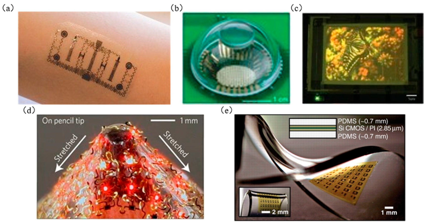
:1. Introduction
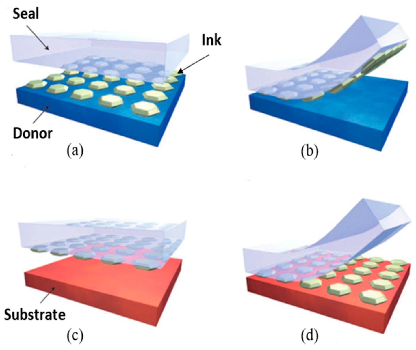
2. Classification of Microtransfer Printing Methods
2.1. Kinetic Control Transfer Printing
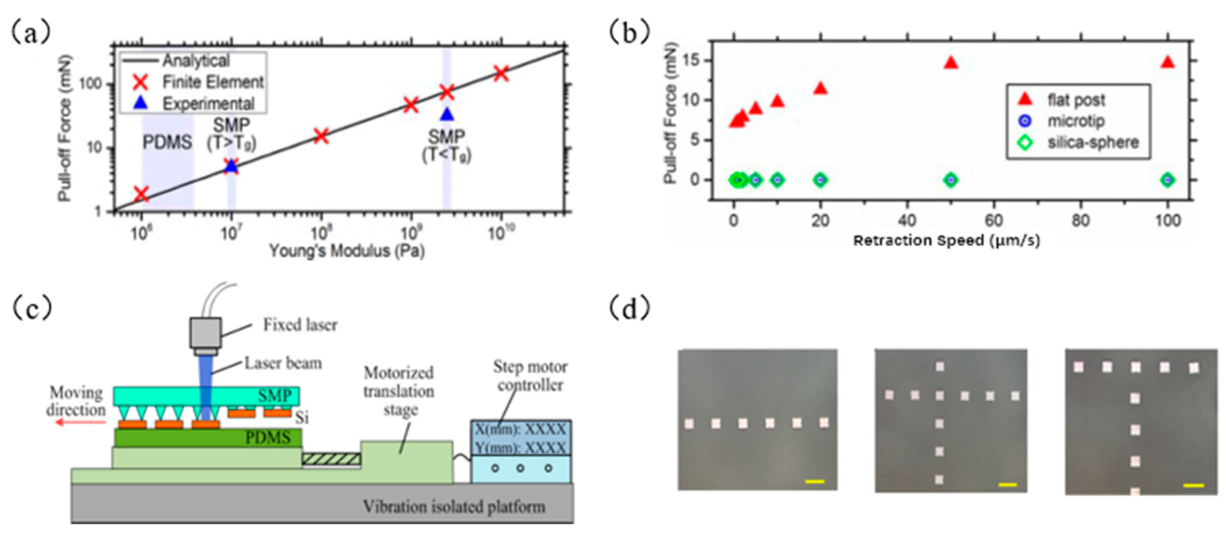
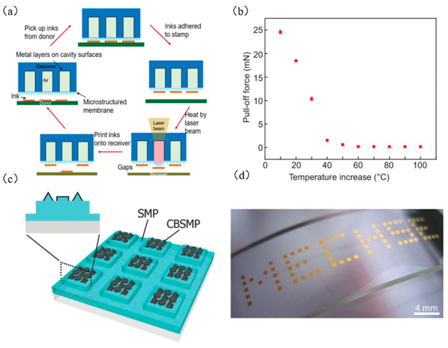
2.2. Laser Control Seal Temperature Transfer Printing
2.3. Microstructure Seal to Assist in Transfer Printing
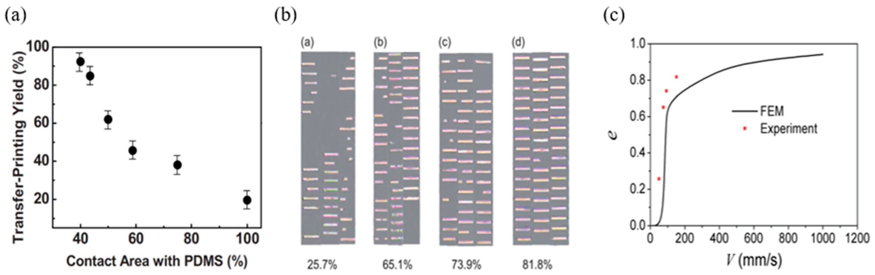
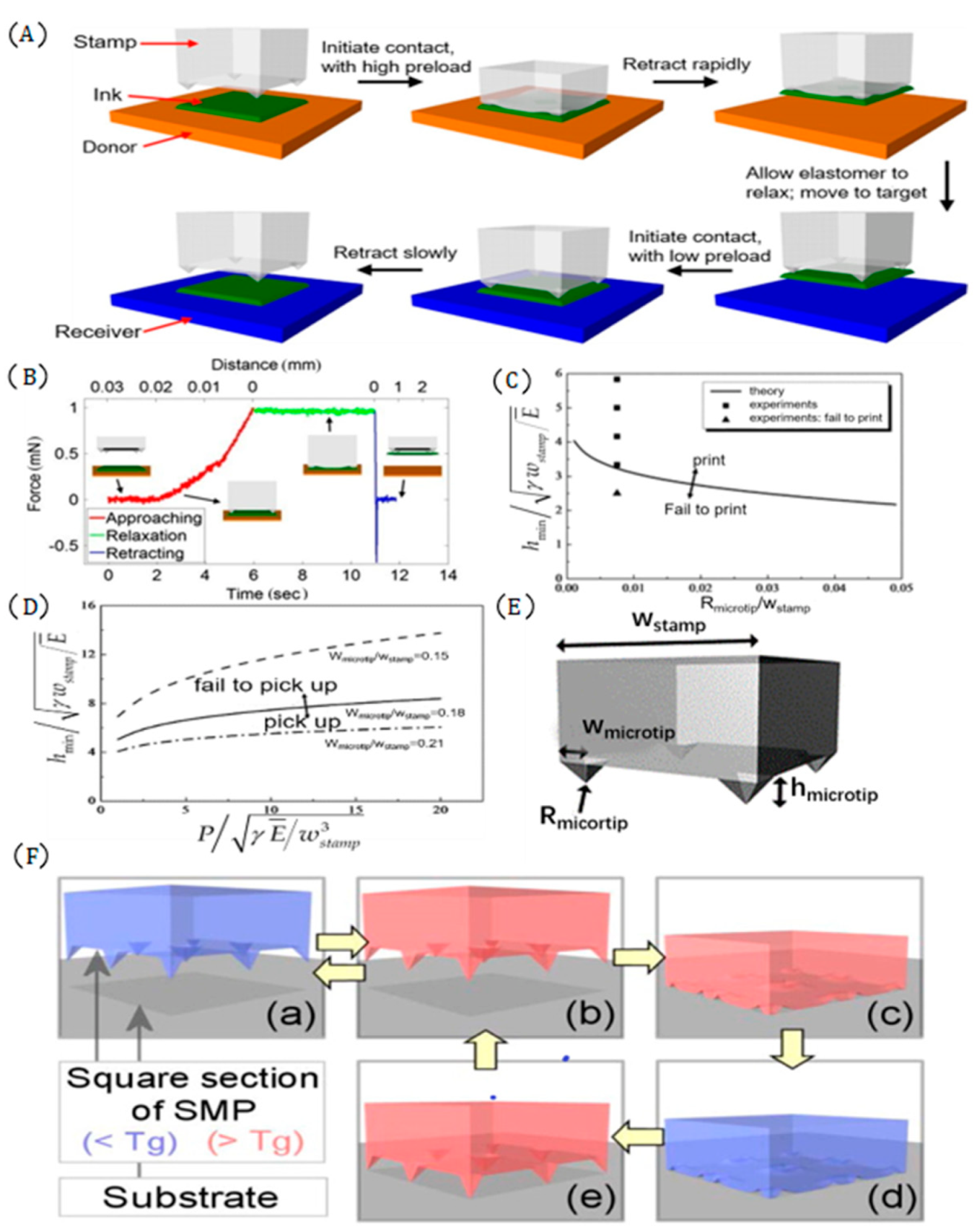
2.3.1. Oblique Column Structure
2.3.2. Pyramid Structure
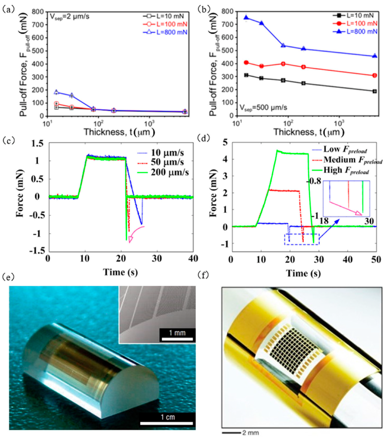
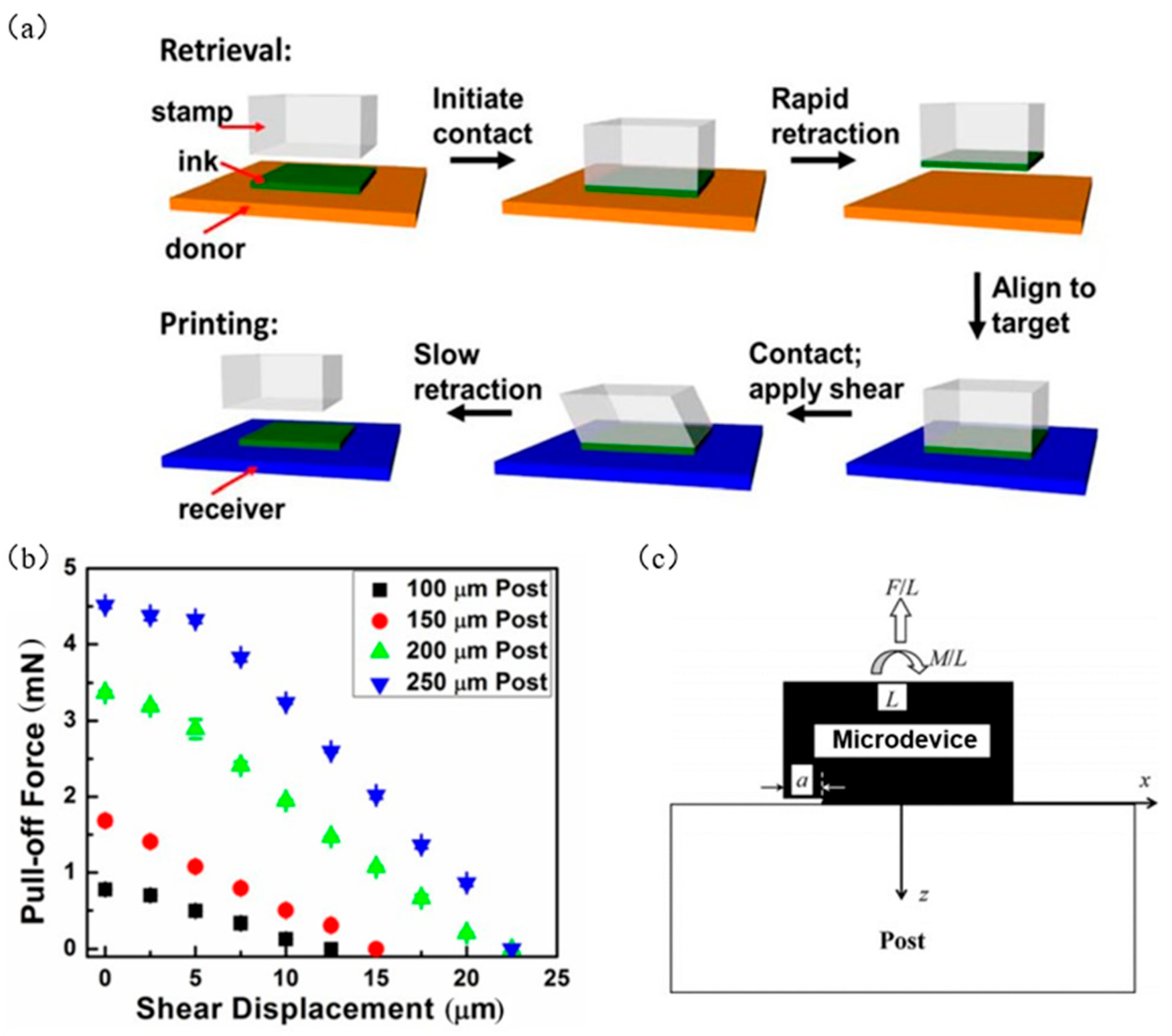
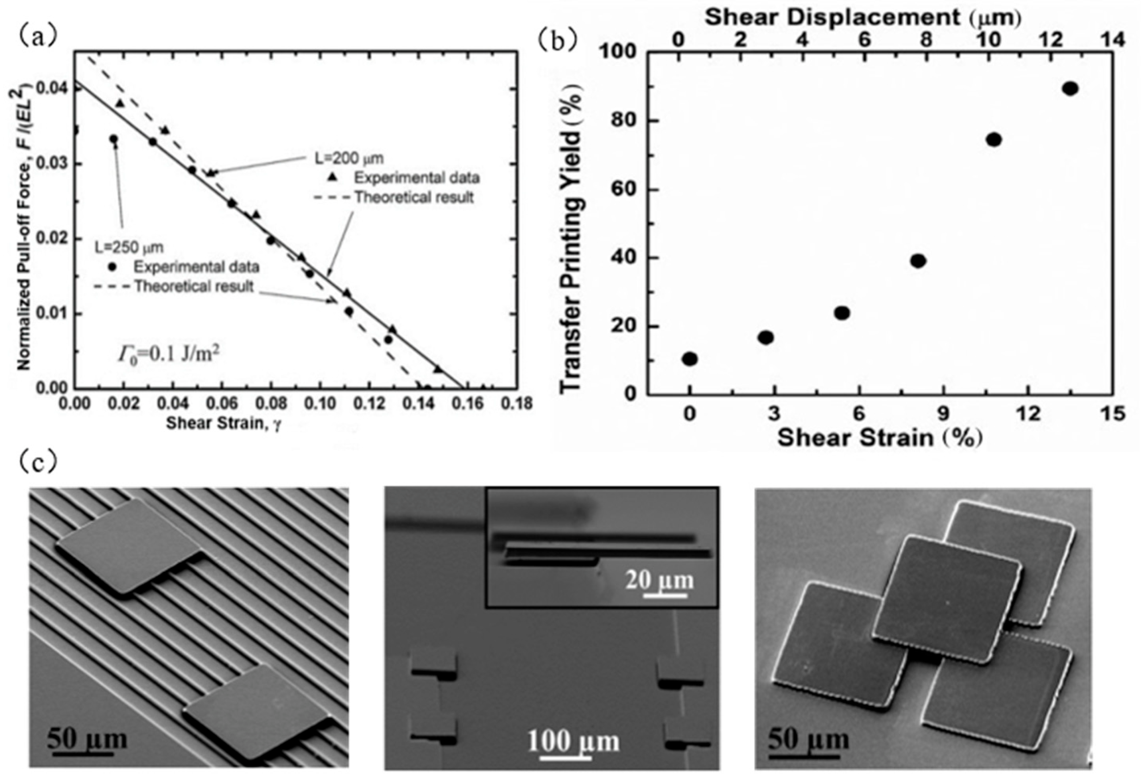
2.4. Transfer Printing with an Applied Shear Load
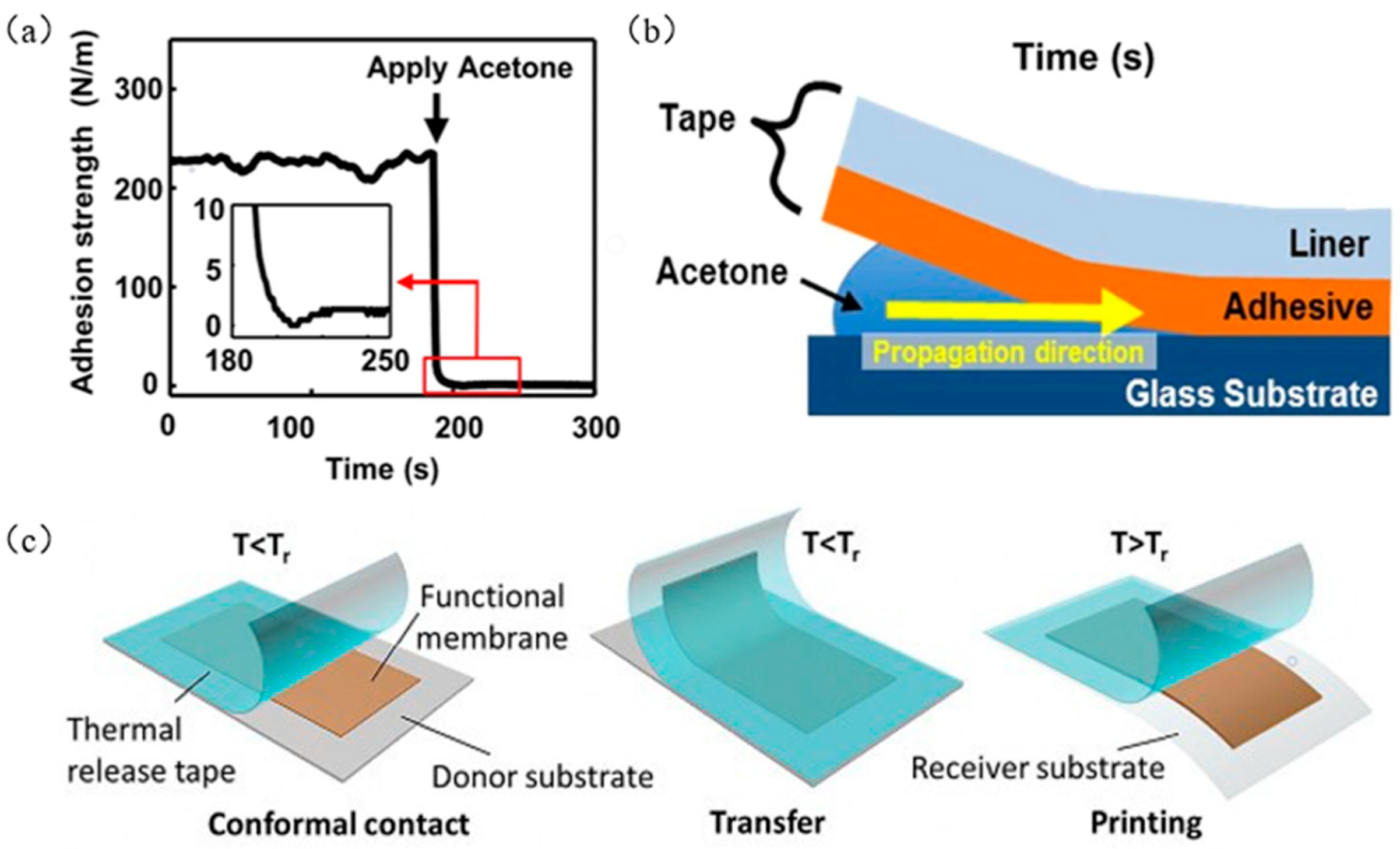
2.5. Tape-Assisted Transfer Printing
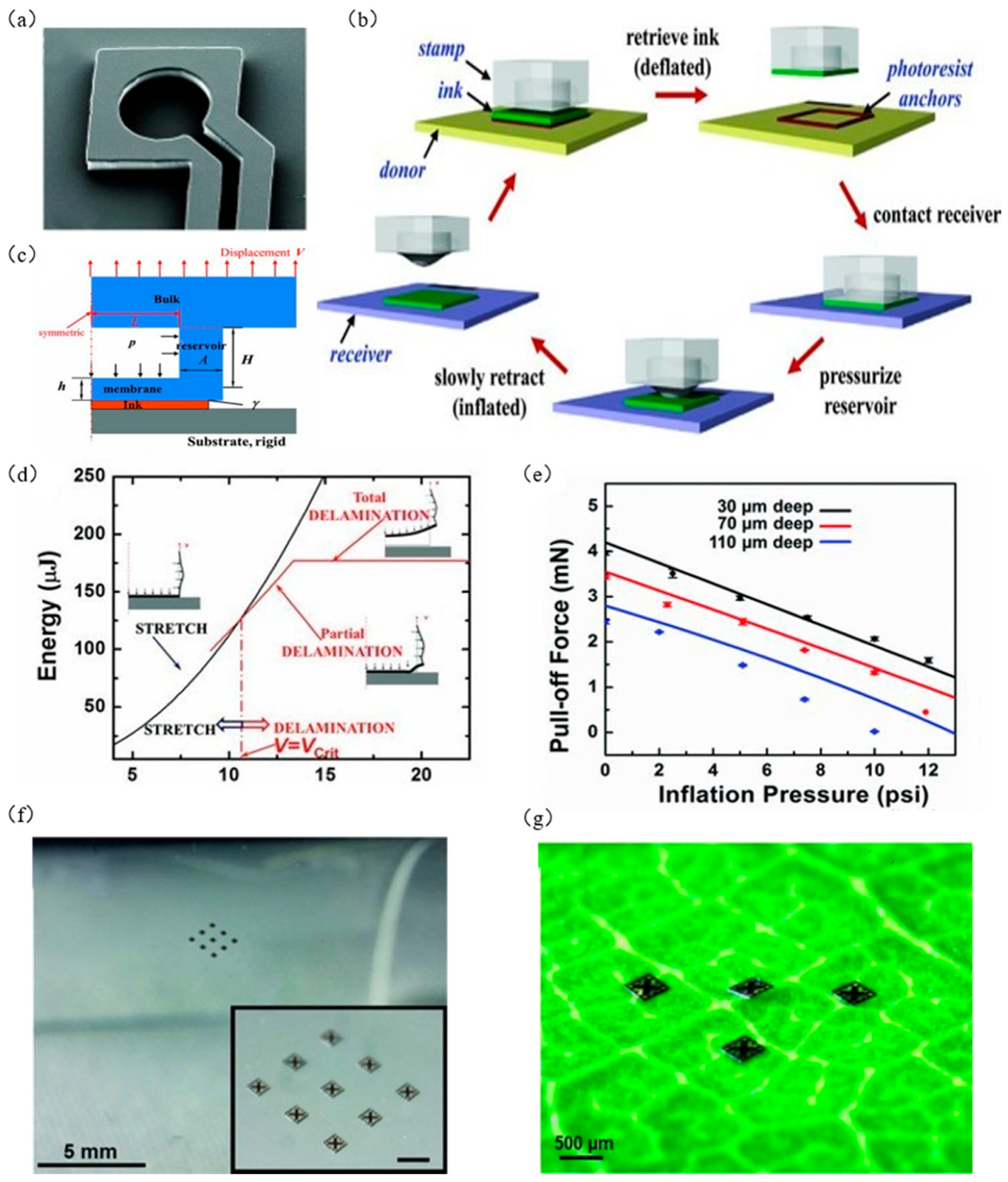
2.6. Transfer Printing with Seal Inflatable
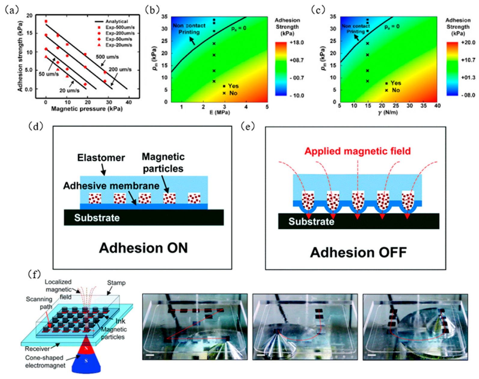
2.7. Magnetic Control Transfer Printing
3. Conclusions and Outlook
Author Contributions
Funding
Institutional Review Board Statement
Informed Consent Statement
Conflicts of Interest
References
- Rogers, J.A.; Nuzzo, R.G. Recent progress in soft lithography. Mater. Today 2005, 8, 50–56. [Google Scholar] [CrossRef]
- Menard, E.; Meitl, M.A.; Sun, Y.; Park, J.U.; Shir, D.J.L.; Nam, Y.S.; Jeon, S.; Rogers, J.A. Micro-and nanopatterning techniques for organic electronic and optoelectronic systems. Chem. Rev. 2007, 107, 1117–1160. [Google Scholar] [CrossRef] [PubMed]
- Yan, Z.; Han, M.; Shi, Y.; Badea, A.; Yang, Y.; Kulkarni, A.; Hanson, E.; Kandel, M.E.; Wen, X.; Zhang, F.; et al. Three-dimensional mesostructures as high-temperature growth templates, electronic cellular scaffolds, and self-propelled microrobots. Proc. Nat. Acad. Sci. USA 2017, 114, E9455–E9464. [Google Scholar] [CrossRef] [Green Version]
- Saeidpourazar, R.; Sangid, M.D.; Rogers, J.A.; Ferreira, P.M. A prototype printer for laser driven micro-transfer printing. J. Manuf. Proc. 2012, 14, 416–424. [Google Scholar] [CrossRef]
- Loo, Y.L.; Willett, R.L.; Baldwin, K.W.; Rogers, J.A. Interfacial chemistries for nanoscale transfer printing. J. Am. Soc. 2002, 124, 7654–7655. [Google Scholar] [CrossRef]
- Smythe, E.J.; Dickey, M.D.; Whitesides, G.M.; Capasso, F. A technique to transfer metallic nanoscale patterns to small and non-planar surfaces. ACS Nano 2009, 3, 59–65. [Google Scholar] [CrossRef] [Green Version]
- Baca, A.J.; Ahn, J.H.; Sun, Y.; Meitl, M.A.; Menard, E.; Kim, H.S.; Choi, W.M.; Kim, D.H.; Huang, Y.; Rogers, J.A. Semiconductor wires and ribbons for high-performance flexible electronics. Angew. Chem. Int. Ed. 2008, 47, 5524–5542. [Google Scholar] [CrossRef] [PubMed]
- Felmet, K.; Loo, Y.L.; Sun, Y. Patterning conductive copper by nanotransfer printing. Appl. Phys. Lett. 2004, 85, 3316–3318. [Google Scholar] [CrossRef]
- Schmid, H.; Wolf, H.; Allenspach, R.; Riel, H.; Karg, S.; Michel, B.; Delamarche, E. Preparation of metallic films on elastomeric seals and their application for contact processing and contact printing. Adv. Funct. Mater. 2003, 13, 145–153. [Google Scholar] [CrossRef]
- Hwang, S.W.; Tao, H.; Kim, D.H.; Cheng, H.; Song, J.K.; Rill, E.; Brenckle, M.A.; Panilaitis, B.; Won, S.M.; Kim, Y.S. A physically transient form of silicon electronics. Science 2012, 337, 1640–1644. [Google Scholar] [CrossRef] [Green Version]
- Menard, E.; Lee, K.J.; Khang, D.Y.; Nuzzo, R.G.; Rogers, J.A. A printable form of silicon for high performance thin film transistors on plastic substrates. Appl. Phys. Lett. 2004, 84, 5398–5400. [Google Scholar] [CrossRef] [Green Version]
- Suh, D.; Choi, S.J.; Lee, H.H. Rigiflex lithography for nanostructure transfer. Adv. Mater. 2005, 17, 1554–1560. [Google Scholar] [CrossRef]
- Hines, D.; Mezhenny, S.; Breban, M.; Williams, E.; Ballarotto, V.; Esen, G.; Southard, A.; Fuhrer, M. Nanotransfer printing of organic and carbon nanotube thin-film transistors on plastic substrates. Appl. Phys. Lett. 2005, 86, 163101. [Google Scholar] [CrossRef] [Green Version]
- Ahn, H.; Lee, K.J.; Childs, W.R.; Rogers, J.A.; Nuzzo, R.G.; Shim, A.J. Micron and submicron patterning of polydimethylsiloxane resists on electronic materials by decal transfer lithography and reactive ion-beam etching: Application to the fabrication of high-mobility, thin-film transistors. J. Appl. Phys. 2006, 100, 084907. [Google Scholar] [CrossRef] [Green Version]
- Childs, W.R.; Nuzzo, R.G. Large-area patterning of coinage-metal thin films using decal transfer lithography. Langmuir 2005, 21, 195–202. [Google Scholar] [CrossRef]
- Choi, J.H.; Kim, K.H.; Choi, S.J.; Lee, H.H. Whole device printing for full colour displays with organic light emitting diodes. Nanotechnology 2006, 17, 2246. [Google Scholar] [CrossRef]
- Blanchet, G.B.; Fincher, C.R.; Gao, F. Polyaniline nanotube composites: A high-resolution printable conductor. Appl. Phys. Lett. 2003, 82, 1290–1292. [Google Scholar] [CrossRef]
- Carlson, A.; Bowen, A.M.; Huang, Y.; Nuzzo, R.G.; Rogers, J.A. Transfer printing techniques for materials assembly and micro/nanodevice fabrication. Adv. Mater. 2012, 24, 5284–5318. [Google Scholar] [CrossRef] [PubMed]
- Choi, C.; Choi, M.K.; Liu, S.; Kim, M.S.; Park, O.K.; Im, C.; Kim, J.; Qin, X.; Lee, G.J.; Cho, K.W. Human eye-inspired soft optoelectronic device using high-density MoS2-graphene curved image sensor array. Nat. Commun. 2017, 8, 1664. [Google Scholar] [CrossRef] [Green Version]
- Wang, J.; Xie, J.; Zong, C.; Han, X.; Ji, H.; Zhao, J.; Lu, C. Surface treatment-assisted switchable transfer printing on polydimethylsiloxane films. J. Mater. Chem. C 2016, 4, 3467–3476. [Google Scholar] [CrossRef]
- Yeom, J.; Shannon, M.A. Detachment Lithography of Photosensitive Polymers: A Route to Fabricating Three-Dimensional Structures. Adv. Funct. Mater. 2010, 20, 289–295. [Google Scholar] [CrossRef]
- Lee, S.; Kang, B.; Keum, H.; Ahmed, N.; Rogers, J.A.; Ferreira, P.M.; Kim, S.; Min, B. Heterogeneously Assembled Metamaterials and Metadevices via 3D Modular Transfer Printing. Sci. Rep. 2016, 6, 27621. [Google Scholar] [CrossRef]
- Lee, K.J.; Lee, J.; Hwang, H.; Reitmeier, Z.J.; Davis, R.F.; Rogers, J.A.; Nuzzo, R.G. A printable form of single-crystalline gallium nitride for flexible optoelectronic systems. Small 2005, 1, 1164–1168. [Google Scholar] [CrossRef]
- Sun, Y.; Kim, H.S.; Menard, E.; Kim, S.; Adesida, I.; Rogers, J.A. Printed arrays of aligned GaAs wires for flexible transistors, diodes, and circuits on plastic substrates. Small 2006, 2, 1330–1334. [Google Scholar] [CrossRef] [PubMed]
- Kim, B.H.; Nam, S.; Oh, N.; Cho, S.Y.; Yu, K.J.; Lee, C.H.; Zhang, J.; Deshpande, K.; Trefonas, P.; Kim, J.H.; et al. Multilayer Transfer Printing for Pixelated, Multicolor Quantum Dot Light-Emitting Diodes. ACS Nano 2016, 10, 4920–4925. [Google Scholar] [CrossRef]
- Yoon, J.; Lee, S.M.; Kang, D.; Meitl, M.A.; Bower, C.A.; Rogers, J.A. Heterogeneously Integrated Optoelectronic Devices Enabled by Micro-Transfer Printing. Adv. Opt. Mater. 2015, 3, 1313–1335. [Google Scholar] [CrossRef]
- Kim, B.H.; Kim, J.H.; Persano, L.; Hwang, S.W.; Lee, S.; Lee, J.; Yu, Y.; Kang, Y.; Won, S.M.; Koo, J.; et al. Dry Transient Electronic Systems by Use of Materials that Sublime. Adv. Funct. Mater. 2017, 27, 1606008. [Google Scholar] [CrossRef]
- Prevatte, C.; Guven, I.; Ghosal, K.; Gomez, D.; Moore, T.; Bonafede, S.; Raymond, B.; Trindade, A.J.; Fecioru, A.; Kneeburg, D.; et al. Pressure activated interconnection of micro transfer printed components. Appl. Phys. Lett. 2016, 108, 203503. [Google Scholar] [CrossRef]
- Ahmed, N.; Dagdeviren, C.; Rogers, J.A.; Ferreira, P.M. Active Polymeric Composite Membranes for Localized Actuation and Sensing in Microtransfer Printing. J. Microelectromech. Syst. 2015, 24, 1016–1028. [Google Scholar] [CrossRef]
- Su, C.; Lin, Y.; Shih, T.M.; Lu, H.; Gao, Y.; Huang, J.E.; Lu, Y.J.; Wu, T.; Chen, Z.; Guo, W. Investigation on Key Parameters in the Fabrication of Seals for Transfer Printing of Micro Devices. Appl. Sci. 2020, 10, 4604. [Google Scholar] [CrossRef]
- Yu, K.J.; Yan, Z.; Han, M.; Rogers, J.A. Inorganic semiconducting materials for flexible and stretchable electronics. npj Flex. Electron. 2017, 1, 4. [Google Scholar] [CrossRef] [Green Version]
- Kim, D.H.; Lu, N.; Ma, R.; Kim, Y.S.; Kim, R.H.; Wang, S.; Wu, J.; Won, S.M.; Tao, H.; Islam, A. Epidermal electronics. Science 2011, 333, 838–843. [Google Scholar] [CrossRef] [Green Version]
- Kabiri Ameri, S.; Ho, R.; Jang, H.; Tao, L.; Wang, Y.; Wang, L.; Schnyer, D.M.; Akinwande, D.; Lu, N. Graphene electronic tattoo sensors. ACS Nano 2017, 11, 7634–7641. [Google Scholar] [CrossRef]
- Yang, S.; Chen, Y.C.; Nicolini, L.; Pasupathy, P.; Sacks, J.; Su, B.; Yang, R.; Sanchez, D.; Chang, Y.F.; Wang, P. “Cut-and-paste” manufacture of multiparametric epidermal sensor systems. Adv. Mater. 2015, 27, 6423–6430. [Google Scholar] [CrossRef] [PubMed]
- Park, J.; Ha, M.; Yu, S.; Jung, B. Fabrication of various optical tissue phantoms by the spin-coating method. J. Biomed. Opt. 2016, 21, 65008. [Google Scholar] [CrossRef]
- Kim, S.J.; Cho, K.W.; Cho, H.R.; Wang, L.; Park, S.Y.; Lee, S.E.; Hyeon, T.; Lu, N.; Choi, S.H.; Kim, D.H. Stretchable and Transparent Biointerface Using Cell-Sheet-Graphene Hybrid for Electrophysiology and Therapy of Skeletal Muscle. Adv. Funct. Mater. 2016, 26, 3207–3217. [Google Scholar] [CrossRef]
- Jiang, D.; Feng, X.; Qu, B.; Wang, Y.; Fang, D. Rate-dependent interaction between thin films and interfaces during micro/nanoscale transfer printing. Soft Matter 2012, 8, 418–423. [Google Scholar] [CrossRef]
- Jung, Y.H.; Chang, T.H.; Zhang, H.; Yao, C.; Zheng, Q.; Yang, V.W.; Mi, H.; Kim, M.; Cho, S.J.; Park, D.W.; et al. High-performance green flexible electronics based on biodegradable cellulose nanofibril paper. Nat. Commun. 2015, 6, 7170. [Google Scholar] [CrossRef] [PubMed]
- Luo, H.; Wang, C.; Linghu, C.; Yu, K.; Wang, C.; Song, J. Laser-driven programmable non-contact transfer printing of objects onto arbitrary receivers via an active elastomeric microstructured seal. Natl. Sci. Rev. 2020, 7, 296–304. [Google Scholar] [CrossRef] [Green Version]
- Park, S.I.; Xiong, Y.; Kim, R.H.; Elvikis, P.; Meitl, M.; Kim, D.H.; Wu, J.; Yoon, J.; Yu, C.J.; Liu, Z. Printed assemblies of inorganic light-emitting diodes for deformable and semitransparent displays. Science 2009, 325, 977–981. [Google Scholar] [CrossRef] [Green Version]
- Gao, W.; Emaminejad, S.; Nyein, H.Y.Y.; Challa, S.; Chen, K.; Peck, A.; Fahad, H.M.; Ota, H.; Shiraki, H.; Kiriya, D. Fully in-tegrated wearable sensor arrays for multiplexed in situ perspiration analysis. Nature 2016, 529, 509–514. [Google Scholar] [CrossRef] [PubMed] [Green Version]
- Lee, H.; Song, C.; Hong, Y.S.; Kim, M.S.; Cho, H.R.; Kang, T.; Shin, K.; Choi, S.H.; Hyeon, T.; Kim, D.H. Wearable/disposable sweat-based glucose monitoring device with multistage transdermal drug delivery module. Sci. Adv. 2017, 3, e1601314. [Google Scholar] [CrossRef] [Green Version]
- Kim, S.J.; Cho, H.R.; Cho, K.W.; Qiao, S.; Rhim, J.S.; Soh, M.; Kim, T.; Choi, M.K.; Choi, C.; Park, I.; et al. Multifunctional Cell-Culture Platform for Aligned Cell Sheet Monitoring, Transfer Printing, and Therapy. ACS Nano 2015, 9, 2677–2688. [Google Scholar] [CrossRef]
- Choi, M.K.; Yang, J.; Kim, D.C.; Dai, Z.; Kim, J.; Seung, H.; Kale, V.S.; Sung, S.J.; Park, C.R.; Lu, N. Extremely vivid, highly transparent, and ultrathin quantum dot light-emitting diodes. Adv. Mater. 2018, 30, 1703279. [Google Scholar] [CrossRef] [PubMed]
- Choi, M.K.; Yang, J.; Kang, K.; Kim, D.C.; Choi, C.; Park, C.; Kim, S.J.; Chae, S.I.; Kim, T.H.; Kim, J.H. Wearable red–green–blue quantum dot light-emitting diode array using high-resolution intaglio transfer printing. Nat. Commun. 2015, 6, 7149. [Google Scholar] [CrossRef] [PubMed]
- Cho, S.; Kim, N.; Song, K.; Lee, J. Adhesiveless Transfer Printing of Ultrathin Microscale Semiconductor Materials by Controlling the Bending Radius of an Elastomeric Seal. Langmuir 2016, 32, 7951–7957. [Google Scholar] [CrossRef]
- Jang, K.I.; Chung, H.U.; Xu, S.; Lee, C.H.; Luan, H.; Jeong, J.; Cheng, H.; Kim, G.T.; Han, S.Y.; Lee, J.W.; et al. Soft network composite materials with deterministic and bio-inspired designs. Nat. Commun. 2015, 6, 6566. [Google Scholar] [CrossRef] [PubMed] [Green Version]
- Meitl, M.A.; Zhu, Z.T.; Kumar, V.; Lee, K.J.; Feng, X.; Huang, Y.Y.; Adesida, I.; Nuzzo, R.G.; Rogers, J.A. Transfer printing by kinetic control of adhesion to an elastomeric stamp. Nat. Mater. 2006, 5, 33–38. [Google Scholar] [CrossRef]
- Xu, B.; Akhtar, A.; Liu, Y.; Chen, H.; Yeo, W.H.; Park, S.; Boyce, B.; Kim, H.; Yu, J.; Lai, H.Y. An epidermal stimulation and sensing platform for sensorimotor prosthetic control, management of lower back exertion, and electrical muscle activation. Adv. Mater. 2016, 28, 4462–4471. [Google Scholar] [CrossRef]
- Ko, H.C.; Stoykovich, M.P.; Song, J.; Malyarchuk, V.; Choi, W.M.; Yu, C.J.; Geddes Iii, J.B.; Xiao, J.; Wang, S.; Huang, Y. A hemispherical electronic eye camera based on compressible silicon optoelectronics. Nature 2008, 454, 748–753. [Google Scholar] [CrossRef]
- Kim, T.H.; Cho, K.S.; Lee, E.K.; Lee, S.J.; Chae, J.; Kim, J.W.; Kim, D.H.; Kwon, J.Y.; Amaratunga, G.; Lee, S.Y. Full-colour quantum dot displays fabricated by transfer printing. Nat. Photonics 2011, 5, 176–182. [Google Scholar] [CrossRef]
- Kim, R.H.; Kim, D.H.; Xiao, J.; Kim, B.H.; Park, S.; Panilaitis, B.; Ghaffari, R.; Yao, J.; Li, M.; Liu, Z. Waterproof AlInGaP optoelectronics on stretchable substrates with applications in biomedicine and robotics. Nat. Mater. 2010, 9, 929–937. [Google Scholar] [CrossRef]
- Kim, D.H.; Ahn, J.H.; Choi, W.M.; Kim, H.S.; Kim, T.H.; Song, J.; Huang, Y.Y.; Liu, Z.; Lu, C.; Rogers, J.A. Stretchable and foldable silicon integrated circuits. Science 2008, 320, 507–511. [Google Scholar] [CrossRef] [Green Version]
- Xu, H.; Huskens, J. Versatile seals in microcontact printing: Transferring inks by molecular recognition and from ink reservoirs. Chem. Eur. J. 2010, 16, 2342–2348. [Google Scholar] [CrossRef]
- Wolf, M.P.; Salieb-Beugelaar, G.B.; Hunziker, P. PDMS with designer functionalities—Properties, modifications strategies, and applications. Prog. Polym. Sci. 2018, 83, 97–134. [Google Scholar] [CrossRef]
- Linghu, C.; Zhu, H.; Zhu, J.; Li, C.; Song, J. Mechanics of magnet-controlled transfer printing. Extreme Mech. Lett. 2019, 27, 76–82. [Google Scholar] [CrossRef]
- Huang, Y.; Zheng, N.; Cheng, Z.; Chen, Y.; Lu, B.; Xie, T.; Feng, X. Direct laser writing-based programmable transfer printing via bioinspired shape memory reversible adhesive. ACS Appl. Mater. Interfaces 2016, 8, 35628–35633. [Google Scholar] [CrossRef] [PubMed]
- Liang, C.; Wang, F.; Huo, Z.; Shi, B.; Tian, Y.; Zhang, D. Adhesion performance study of a novel microstructured seal for micro-transfer printing. Soft Matter 2021, 17, 4989–4997. [Google Scholar] [CrossRef]
- Gao, Y.; Li, Y.; Li, R.; Song, J. An accurate thermomechanical model for laser-driven microtransfer printing. J. Appl. Mech. 2017, 84, 64501. [Google Scholar] [CrossRef]
- Wu, J.; Kim, S.; Chen, W.Q.; Carlson, A.; Hwang, K.C.; Huang, Y.G.; Rogers, J.A. Mechanics of reversible adhesion. Soft Matter 2011, 7, 8657–8662. [Google Scholar] [CrossRef]
- Kim, S.; Wu, J.; Carlson, A.; Jin, S.H.; Kovalsky, A.; Glass, P.; Liu, Z.; Ahmed, N.; Elgan, S.L.; Chen, W. Microstructured elastomeric surfaces with reversible adhesion and examples of their use in deterministic assembly by transfer printing. Proc. Nat. Acad. Sci. USA 2010, 107, 17095–17100. [Google Scholar] [CrossRef] [Green Version]
- Yang, S.Y.; Carlson, A.; Cheng, H.; Yu, Q.; Ahmed, N.; Wu, J.; Kim, S.; Sitti, M.; Ferreira, P.M.; Huang, Y. Elastomer surfaces with directionally dependent adhesion strength and their use in transfer printing with continuous roll-to-roll applications. Adv. Mater. 2012, 24, 2117–2122. [Google Scholar] [CrossRef] [PubMed]
- Xue, Y.; Zhang, Y.; Feng, X.; Kim, S.; Rogers, J.A.; Huang, Y. A theoretical model of reversible adhesion in shape memory surface relief structures and its application in transfer printing. J. Mech. Phys. Solids 2015, 77, 27–42. [Google Scholar] [CrossRef]
- Kim, M.S.; Park, J.; Choi, B. Measurement and analysis of micro-scale adhesion for efficient transfer printing. J. Appl. Phys. 2011, 110, 024911. [Google Scholar] [CrossRef]
- Zhang, J.W.; Lin, C.G.; Wang, L.; Zheng, J.Y.; Peng, Y.L.; Duan, D.X. In The influence of elastic modulus on the adhesion of fouling organism to poly (dimethylsiloxane)(PDMS). Adv. Mat. Res. 2011, 152, 1466–1470. [Google Scholar] [CrossRef]
- Jeong, J.; Kim, J.; Song, K.; Autumn, K.; Lee, J. Geckoprinting: Assembly of microelectronic devices on unconventional surfaces by transfer printing with isolated gecko setal arrays. J. R Soc. Interface 2014, 11, 20140627. [Google Scholar] [CrossRef] [PubMed] [Green Version]
- Brodoceanu, D.; Bauer, C.T.; Kroner, E.; Arzt, E.; Kraus, T. Hierarchical bioinspired adhesive surfaces—A review. Bioinspir. Biomim. 2016, 11, 51001. [Google Scholar] [CrossRef] [PubMed]
- Eisenhaure, J.D.; Rhee, S., II; Ala’a, M.; Carlson, A.; Ferreira, P.M.; Kim, S. The use of shape memory polymers for microassembly by transfer printing. J. Microelectromech. Syst. 2014, 23, 1012–1014. [Google Scholar] [CrossRef]
- Linghu, C.; Zhang, S.; Wang, C.; Yu, K.; Li, C.; Zeng, Y.; Zhu, H.; Jin, X.; You, Z.; Song, J. Universal SMP gripper with massive and selective capabilities for multiscaled, arbitrarily shaped objects. Sci. Adv. 2020, 6, eaay5120. [Google Scholar] [CrossRef] [PubMed] [Green Version]
- Liang, C.; Wang, F.; Huo, Z.; Shi, B.; Tian, Y.; Zhao, X.; Zhang, D. Structures, Pull-off force modeling and experimental study of PDMS seal considering preload in micro transfer printing. Int. J. Solids Struct. 2020, 193, 134–140. [Google Scholar] [CrossRef]
- Kim, T.H.; Carlson, A.; Ahn, J.H.; Won, S.M.; Wang, S.; Huang, Y.; Rogers, J.A. Kinetically controlled, adhesiveless transfer printing using microstructured stamps. Appl. Phys. Lett. 2009, 94, 113502. [Google Scholar] [CrossRef] [Green Version]
- Linghu, C.; Wang, C.; Cen, N.; Wu, J.; Lai, Z.; Song, J. Rapidly tunable and highly reversible bio-inspired dry adhesion for transfer printing in air and a vacuum. Soft Matter 2019, 15, 30–37. [Google Scholar] [CrossRef]
- Carlson, A.; Kim-Lee, H.J.; Wu, J.; Elvikis, P.; Cheng, H.; Kovalsky, A.; Elgan, S.; Yu, Q.; Ferreira, P.M.; Huang, Y. Shear-enhanced adhesiveless transfer printing for use in deterministic materials assembly. Appl. Phys. Lett. 2011, 98, 264104. [Google Scholar] [CrossRef] [Green Version]
- Zhou, Z.; Chen, D.; Wang, X.; Jiang, J. Milling positive master for polydimethylsiloxane microfluidic devices: The microfab-rication and roughness issues. Micromachines 2017, 8, 287. [Google Scholar] [CrossRef] [Green Version]
- Sim, K.; Chen, S.; Li, Y.; Kammoun, M.; Peng, Y.; Xu, M.; Gao, Y.; Song, J.; Zhang, Y.; Ardebili, H. High fidelity tape transfer printing based on chemically induced adhesive strength modulation. Sci. Rep. 2015, 5, 16133. [Google Scholar] [CrossRef] [Green Version]
- Yan, Z.; Pan, T.; Xue, M.; Chen, C.; Cui, Y.; Yao, G.; Huang, L.; Liao, F.; Jing, W.; Zhang, H. Thermal release transfer printing for stretchable conformal bioelectronics. Adv. Sci. 2017, 4, 1700251. [Google Scholar] [CrossRef] [PubMed]
- Dong, W.; Cheng, X.; Wang, X. Theoretical and experimental study of tape transfer printing for stretchable electronic fabrication. J. Mech. Med. Biol. 2018, 18, 1850045. [Google Scholar] [CrossRef]
- Feng, X.; Meitl, M.A.; Bowen, A.M.; Huang, Y.; Nuzzo, R.G.; Rogers, J.A. Competing fracture in kinetically controlled transfer printing. Langmuir 2007, 23, 12555–12560. [Google Scholar] [CrossRef]
- Feng, X.; Cheng, H.; Bowen, A.M.; Carlson, A.W.; Nuzzo, R.G.; Rogers, J.A. A finite-deformation mechanics theory for kinetically controlled transfer printing. J. Appl. Mech. 2013, 80, 61023. [Google Scholar] [CrossRef]
- Kim, C.; Yoon, M.A.; Jang, B.; Kim, J.H.; Lee, H.J.; Kim, K.S. Ultimate control of rate-dependent adhesion for reversible transfer process via a thin elastomeric layer. ACS Appl. Mater. 2017, 9, 12886–12892. [Google Scholar] [CrossRef] [PubMed]
- Li, R.; Li, Y.; Lü, C.; Song, J.; Saeidpouraza, R.; Fang, B.; Zhong, Y.; Ferreira, P.M.; Rogers, J.A.; Huang, Y. Thermo-mechanical modeling of laser-driven non-contact transfer printing: Two-dimensional analysis. Soft Matter 2012, 8, 7122–7127. [Google Scholar] [CrossRef]
- Eisenhaure, J.D.; Xie, T.; Varghese, S.; Kim, S. Microstructured shape memory polymer surfaces with reversible dry adhe-sion. ACS Appl. Mater. 2013, 5, 7714–7717. [Google Scholar] [CrossRef]
- Sen, P.; Xiong, Y.; Zhang, Q.; Park, S.; You, W.; Ade, H.; Kudenov, M.W.; O’Connor, B.T. Shear-enhanced transfer printing of conducting polymer thin films. ACS Appl. Mater. 2018, 10, 31560–31567. [Google Scholar] [CrossRef]
- Cheng, H.; Wu, J.; Yu, Q.; Kim-Lee, H.J.; Carlson, A.; Turner, K.T.; Hwang, K.C.; Huang, Y.; Rogers, J.A. An analytical model for shear-enhanced adhesiveless transfer printing. Mech. Res. Commun. 2012, 43, 46–49. [Google Scholar] [CrossRef]
- Carlson, A.; Wang, S.; Elvikis, P.; Ferreira, P.M.; Huang, Y.; Rogers, J.A. Active, programmable elastomeric surfaces with tunable adhesion for deterministic assembly by transfer printing. Adv. Funct. Mater. 2012, 22, 4476–4484. [Google Scholar] [CrossRef]
- Yoon, J.; Jo, S.; Chun, I.S.; Jung, I.; Kim, H.S.; Meitl, M.; Menard, E.; Li, X.; Coleman, J.J.; Paik, U. GaAs photovoltaics and optoelectronics using releasable multilayer epitaxial assemblies. Nature 2010, 465, 329–333. [Google Scholar] [CrossRef]
- Li, R.; Li, Y.; Lü, C.; Song, J.; Saeidpourazar, R.; Fang, B.; Zhong, Y.; Ferreira, P.M.; Rogers, J.A.; Huang, Y. Axisymmetric thermo-mechanical analysis of laser-driven non-contact transfer printing. Int. J. Fract. 2012, 176, 189–194. [Google Scholar] [CrossRef] [Green Version]
- Lee, C.H.; Kim, D.R.; Zheng, X. Fabricating nanowire devices on diverse substrates by simple transfer-printing methods. Proc. Nat. Acad. Sci. USA 2010, 107, 9950–9955. [Google Scholar] [CrossRef] [PubMed] [Green Version]
- Yeo, W.H.; Kim, Y.S.; Lee, J.; Ameen, A.; Shi, L.; Li, M.; Wang, S.; Ma, R.; Jin, S.H.; Kang, Z. Multifunctional epidermal electronics printed directly onto the skin. Adv. Mater. 2013, 25, 2773–2778. [Google Scholar] [CrossRef]
- Jeong, J.W.; Yang, S.R.; Hur, Y.H.; Kim, S.W.; Baek, K.M.; Yim, S.; Jang, H.I.; Park, J.H.; Lee, S.Y.; Park, C.O. High-resolution nanotransfer printing applicable to diverse surfaces via interface-targeted adhesion switching. Nat. Commun. 2014, 5, 5387. [Google Scholar] [CrossRef] [Green Version]


| Seal Category | Seal Material Composition | Elastic Modulus | Glass Transition Temperature | Seal Surface | Maximum Adhesion | Minimum Adhesion | Adhesion Control Mechanism | Corresponding Transfer Method | References |
|---|---|---|---|---|---|---|---|---|---|
| PDMS | By weight ratio of 10: A prepolymer of 1 is mixed with a crosslinker | 1.32–2.97 MPa | −125 °C | Flat seal | 120 | 74 | Control seal peeling speed | Kinetic control transfer printing | [70] |
| Flat seal | 1530 | 128 | [71] | ||||||
| Below 100 °C | Microstructural seal of tiny structure | 312.5 | ≈0.3 | Thermal mismatch occurs between interfaces during laser heating | Laser control seal temperature transfer printing | [4,39] | |||
| −125 °C | Flat seal | 22 | Almost 0 | Magnetic force is used to control the swelling and collapse of the film to achieve the switch between the seal and ink contact area | Magnetic control transfer printing | [72] | |||
| The weight mixing ratio of the prepolymer to the crosslinker is 5:1 | 1.8–2.1 MPa | Pyramidal microstructure | 80 | 0.08 | By changing the seal and ink contact area | Microstructure seal to assist in transfer printing | [61] | ||
| Oblique column microstructure | 100 | 1 | [62] | ||||||
| Flat seal | 85 | 8.5 | Apply a shear load on the seal to adjust the adhesion | Transfer printing with applied shear load | [73] | ||||
| SMP | By weight ratio of 45: 23 epoxy monomer E44 and Jeffamine D230 | 40–60 °C | Flat seal | 3200 | 534 | Thermal mismatch occurs between interfaces during laser heating | Laser control seal temperature transfer printing | [57,68] | |
| Pyramidal microstructure | 2800 | 2.8 | |||||||
| CBSMP | The mole ratio is 1:1:1 EPON 826 (heated-out impurity), Jeffamine D230, and NGDE, which were mixed, and XC72R powdered carbon black was used as additive | Thermal mismatch occurs between interfaces during laser heating | Laser control seal temperature transfer printing | [74] | |||||
| 3M 3850 tape | Flat seal | 880 | Almost 0 | By adding acetone to control the switch of adhesion | Tape-assisted transfer printing | [75] | |||
| Thermal release tape (TRT) | 100 °C | Flat seal | By heating the TRT tape, the adhesive force is irreversibly reduced | Tape-assisted transfer printing | [76] | ||||
| Water-soluble tape (PVA) | Polyvinyl alcohol | 1 GPa | Flat seal | Use PVA water-soluble tape as a sacrificial layer to achieve the effect of reducing the interfacial adhesion energy | Tape-assisted transfer printing | [77] | |||
Publisher’s Note: MDPI stays neutral with regard to jurisdictional claims in published maps and institutional affiliations. |
© 2021 by the authors. Licensee MDPI, Basel, Switzerland. This article is an open access article distributed under the terms and conditions of the Creative Commons Attribution (CC BY) license (https://creativecommons.org/licenses/by/4.0/).
Share and Cite
Zhang, L.; Zhang, C.; Tan, Z.; Tang, J.; Yao, C.; Hao, B. Research Progress of Microtransfer Printing Technology for Flexible Electronic Integrated Manufacturing. Micromachines 2021, 12, 1358. https://doi.org/10.3390/mi12111358
Zhang L, Zhang C, Tan Z, Tang J, Yao C, Hao B. Research Progress of Microtransfer Printing Technology for Flexible Electronic Integrated Manufacturing. Micromachines. 2021; 12(11):1358. https://doi.org/10.3390/mi12111358
Chicago/Turabian StyleZhang, Li, Chong Zhang, Zheng Tan, Jingrong Tang, Chi Yao, and Bo Hao. 2021. "Research Progress of Microtransfer Printing Technology for Flexible Electronic Integrated Manufacturing" Micromachines 12, no. 11: 1358. https://doi.org/10.3390/mi12111358
APA StyleZhang, L., Zhang, C., Tan, Z., Tang, J., Yao, C., & Hao, B. (2021). Research Progress of Microtransfer Printing Technology for Flexible Electronic Integrated Manufacturing. Micromachines, 12(11), 1358. https://doi.org/10.3390/mi12111358