
Efficient Surrogate Modeling and Design Optimization of Compact Integrated On-Chip Inductors Based on Multi-Fidelity EM Simulation Models


Abstract
:1. Introduction
2. Integrated On-Chip Inductors: Design Challenges and Simulation Models
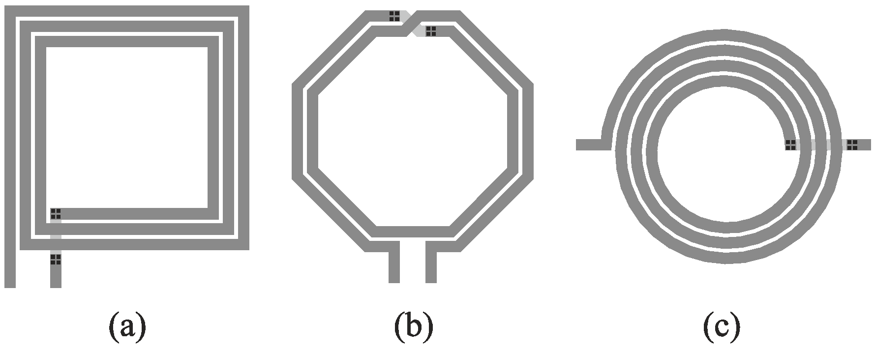
2.1. Integrated On-Chip Inductors: Typical Structures and Applications
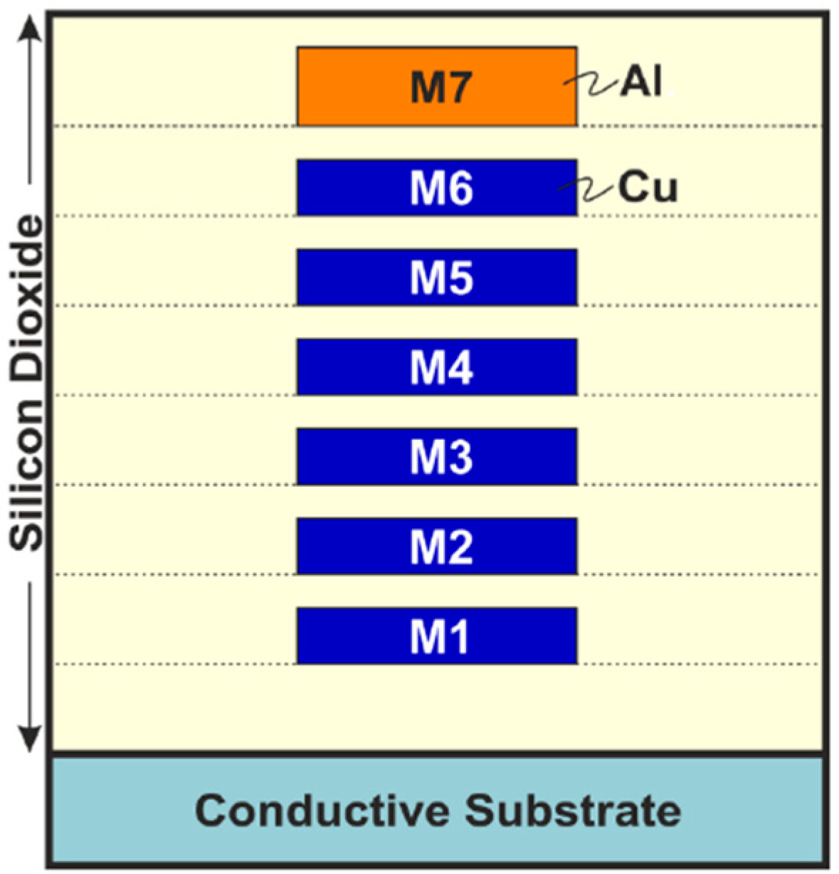
2.2. Computational Models of Integrated Inductors
2.3. Design Challenges
3. Efficient Surrogate Modeling and Design Optimization
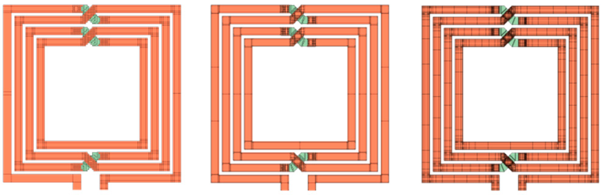
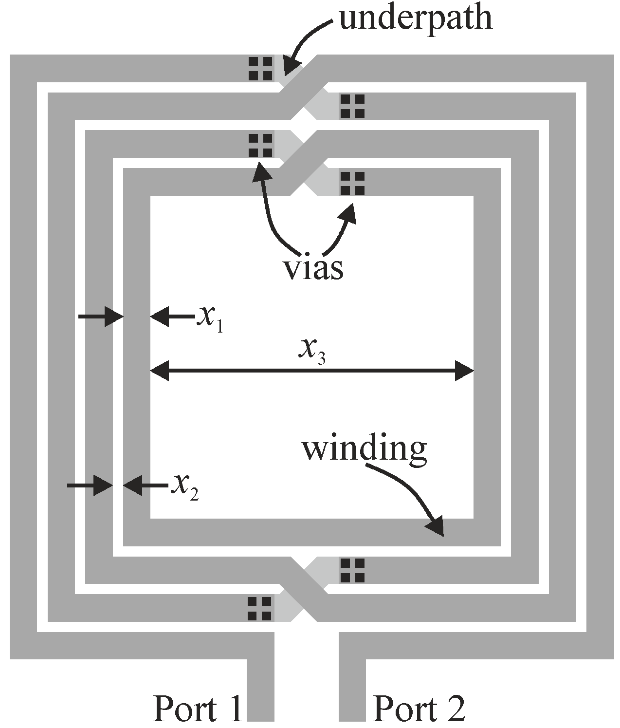
3.1. Design Case
3.2. Surrogate Modeling Using Response Surface Approximation and Space Mapping
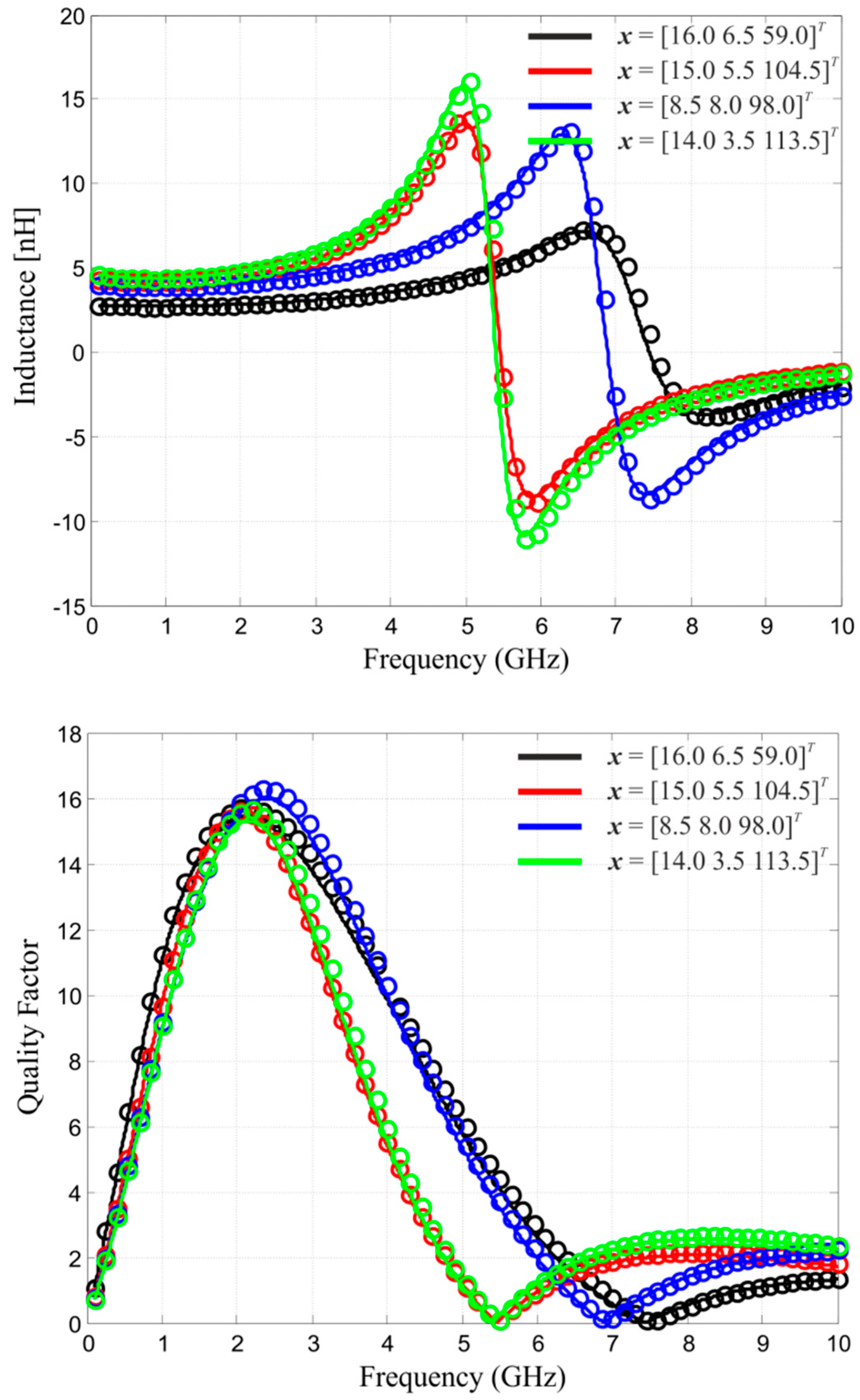
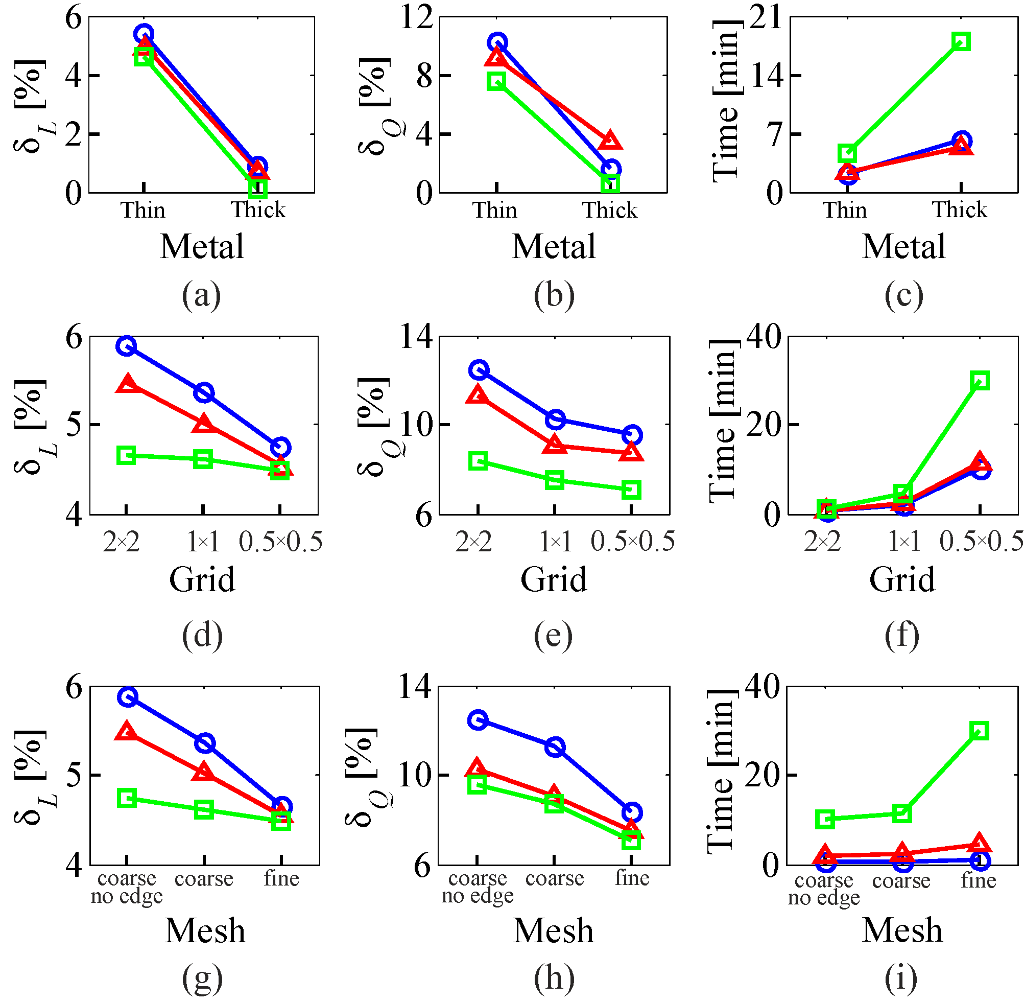
3.3. Numerical Results
3.4. Inductor Design Optimization Application Example
4. Multi-Fidelity Design Optimization of Compact On-Chip Inductors
4.1. Design Case
4.2. Multi-Fidelity Optimization Algorithm
4.3. Numerical Results
5. Discussion and Conclusions
Funding
Conflicts of Interest
References
- Leroux, P.; Steyaert, M. High-performance 5.2 GHz LNA with on-chip inductor to provide ESD protection. Electron. Lett. 2001, 37, 467–469. [Google Scholar] [CrossRef]
- Lin, K.-C.; Chiou, H.-K.; Wu, P.-C.; Chen, W.-H.; Ko, C.-L.; Juang, Y.-Z. 2.4-GHz Complementary Metal Oxide Semiconductor Power Amplifier Using High-Quality Factor Wafer-Level Bondwire Spiral Inductor. IEEE Trans. Compon. Packag. Manuf. Technol. 2013, 3, 1286–1292. [Google Scholar] [CrossRef]
- Chen, C.-H.; Chiang, P.-Y.; Jou, C.F. A Low Voltage Mixer with Improved Noise Figure. IEEE Microw. Wirel. Compon. Lett. 2009, 19, 92–94. [Google Scholar] [CrossRef]
- Grau, G.; Langmann, U.; Winkler, W.; Knoll, D.; Osten, J.; Pressel, K. A Current-Folded Up-Conversion Mixer and VCO with Center-Tapped Inductor in a SiGe-HBT Technology for 5-GHz Wireless LAN Applications. IEEE J. Solid-State Circuits 2000, 35, 1345–1352. [Google Scholar] [CrossRef]
- Aguilera, J.; Berenguer, R. Design and Test of Integrated Inductors for RF Applications; Kluwer Academic Publishers: New York, NY, USA, 2004. [Google Scholar]
- Lopez-Villegas, J.; Samitier, J.; Cane, C.; Losantos, P.; Bausells, J. Improvement of the Quality Factor of RF Integrated Inductors by Layout Optimization. IEEE Trans. Microw. Theory Tech. 2000, 48, 76–83. [Google Scholar] [CrossRef] [Green Version]
- Yue, C.P.; Wong, S.S. On-chip spiral inductors with patterned ground shields for Si-based RF IC’s. IEEE J. Solid-State Circuits 1998, 33, 743–752. [Google Scholar] [CrossRef]
- Wojnowski, M.; Issakov, V.; Knoblinger, G.; Pressel, K.; Sommer, G.; Weigel, R. High-Q Inductors Embedded in the Fan-Out Area of an Ewlb. IEEE Trans. Compon. Packag. Manuf. Technol. 2012, 2, 1280–1292. [Google Scholar] [CrossRef]
- Cao, Y.; Groves, R.A.; Huang, X.; Zamdmer, N.D.; Plouchart, J.-O.; Wachnik, R.A.; King, T.-J.; Hu, C. Frequency-Independent Equivalent-Circuit Model for On-Chip Spiral Inductor. IEEE J. Solid-State Circuits 2003, 38, 419–426. [Google Scholar] [CrossRef]
- Arcioni, P.; Castello, R.; Perregrini, L.; Sacchi, E.; Svelto, F. An Innovative Modelization of Loss Mechanism in Silicon Integrated Inductors. IEEE Trans. Circuits Syst.–II Analog. Digit. Signal Process. 1999, 46, 1453–1460. [Google Scholar] [CrossRef]
- Fakhfakh, M.; Tlelo-Cuautle, E.; Siarry, P. Computational Intelligence in Analog and Mixed-Signal (AMS) and Radio-Frequency (RF) Circuit Design; Springer: Berlin/Heidelberg, Germany, 2015. [Google Scholar]
- Niknejad, A.M.; Meyer, R.G. Analysis, Design, and Optimization of Spiral Inductors and Transformers for Si RF IC’s. IEEE J. Solid-State Circuits 1998, 33, 1470–1481. [Google Scholar] [CrossRef] [Green Version]
- Aguilera, J.; de Nó, J.; García-Alonso, A.; Oehler, F.; Hein, H.; Sauerer, J. A guide for on-chip inductor design in a conventional CMOS process for RF applications. Appl. Microw. Wirel. 2001, 13, 56–65. [Google Scholar]
- Koutsoyannopoulos, Y.K.; Papananos, Y. Systematic Analysis and Modeling of Integrated Inductors and Transformers in RF IC Design. IEEE Trans. Circuits Syst.–II Analog. Digit. Signal Process. 2000, 47, 699–713. [Google Scholar] [CrossRef] [Green Version]
- Hershenson, M.; Mohan, S.S.; Boyd, S.P.; Lee, T.H. Optimization of Inductor Circuits via Geometric Programming. In Proceedings of the 36th Design Automation Conference, New Orleans, LA, USA, 21–25 June 1999; pp. 994–998. [Google Scholar]
- Zhan, Y.; Sapatnekar, S.S. Optimization of Integrated Spiral Inductors Using Sequential Quadratic Programming. In Proceedings of the Design, Automation and Test in Europe Conference and Exhibition, Paris, France, 16–20 February 2004; pp. 622–627. [Google Scholar]
- Nieuwoudt, A.; Massoud, Y. Multi-level approach for integrated spiral inductor optimization. In Proceedings of the 42th Design Automation Conference, San Diego, CA, USA, 13–17 June 2005; pp. 648–651. [Google Scholar]
- Koziel, S.; Leifsson, L. Surrogate-Based Modeling and Optimization: Applications in Engineering; Springer: Berlin/Heidelberg, Germany, 2013. [Google Scholar]
- Yu, W.; Bandler, J.W. Optimization of spiral inductor on silicon using space mapping. In Proceedings of the 2006 IEEE MTT-S International Microwave Symposium Digest, San Francisco, CA, USA, 11–16 June 2006; IEEE: New York, NY, USA, 2006; pp. 1085–1088. [Google Scholar]
- Bandler, J.W.; Cheng, Q.S.; Nikolova, N.K.; Ismail, M.A. Implicit space mapping optimization exploiting preassigned parameters. IEEE Trans. Microw. Theory Tech. 2004, 52, 378–385. [Google Scholar] [CrossRef]
- Koziel, S.; Cheng, Q.S.; Bandler, J.W. Space mapping. IEEE Microw. Mag. 2008, 9, 46–57. [Google Scholar] [CrossRef]
- Kurgan, P.; Koziel, S.; Bandler, J.W. Low-cost EM-driven surrogate modeling and optimization of planar inductors. In Proceedings of the 2015 IEEE MTT-S International Microwave Symposium, Phoenix, AZ, USA, 17–22 May 2015; IEEE: New York, NY, USA, 2015; pp. 1–3. [Google Scholar]
- Caverly, R. CMOS RFIC Design Principles; Artech House: Norwood, MA, USA, 2007. [Google Scholar]
- Hella, M.M.; Ismail, M. RF CMOS Power Amplifiers: Theory, Design and Implementation; Kluwer Academic Publishers: New York, NY, USA, 2002. [Google Scholar]
- Koziel, S.; Yang, X.S.; S, X.; Zhang, Q.J. Simulation-Driven Design Optimization and Modeling for Microwave Engineering; College Press: Imperial, UK, 2012. [Google Scholar]
- Sonnet Em, Version 14.54; Sonnet Software: North Syracuse, NY, USA, 2013.
- Bunch, R.L.; Sanderson, D.I.; Raman, S. Quality Factor and Inductance in Differential IC Implementations. IEEE Microw. Mag. 2002, 3, 82–92. [Google Scholar] [CrossRef]
- Murphy, O.H.; McCarthy, K.G.; Delabie, C.J.P.; Murphy, A.C.; Murphy, P.J. Design of multiple-metal stacked inductors incorporating an extended physical model. IEEE Trans. Microw. Theory Tech. 2005, 53, 2063–2072. [Google Scholar] [CrossRef]
- Haobijam, G.; Paily, R. Efficient optimization of integrated spiral inductor with bounding of layout design parameters. Analog. Integr. Circuits Signal Process. 2007, 51, 131–140. [Google Scholar] [CrossRef]
- Koziel, S.; Bandler, J.W.; Madsen, K. Towards a rigorous formulation of the space mapping technique for engineering design. IEEE Int. Symp. Circuits Syst. 2005, 1, 5605–5608. [Google Scholar]
- Queipo, N.V.; Haftka, R.T.; Shyy, W.; Goel, T.; Vaidynathan, R.; Tucker, P.K. Surrogate based analysis and optimization. Prog. Aerosp. Sci. 2005, 41, 1–28. [Google Scholar] [CrossRef] [Green Version]
- Cheng, Q.S.; Koziel, S.; Bandler, J.W. Simplified space mapping approach to enhancement of microwave device models. Int. J. RF Microw. Comput.-Aided Eng. 2006, 16, 518–535. [Google Scholar] [CrossRef]
- Liu, T.; Zhang, W.; Yu, Z. Modeling of spiral inductors using artificial neural network. In Proceedings of the IEEE International Joint Conference on Neural Networks, Montreal, QC, Canada, 31 July–4 August 2005; pp. 2353–2358. [Google Scholar]
- Wang, Y.; Franzon, P.D. RFIC IP redesign and reuse through surrogate based machine learning method. In Proceedings of the 2018 IEEE MTT-S International Conference on Numerical Electromagnetic and Multiphysics Modeling and Optimization, Reykjavik, Iceland, 8–10 August 2018; pp. 1–4. [Google Scholar]
- Wang, H.; Sun, L.; Liu, J.; Zou, H.; Yu, Z.; Gao, J. Transfer function analysis and broadband scalable model for on-chip spiral inductors. IEEE Trans. Microw. Theory Techn. 2011, 59, 1696–1708. [Google Scholar] [CrossRef]
- Sanderson, D.I.; Rautio, J.C.; Groves, R.A.; Raman, S. Accurate modeling of monolithic inductors using conformal meshing for reduced computation. IEEE Microw. Mag. 2003, 4, 87–96. [Google Scholar] [CrossRef]
- Koziel, S.; Ogurtsov, S. Robust multi-fidelity simulation-driven design optimization of microwave structures. In Proceedings of the 2010 IEEE MTT-S International Microwave Symposium Digest, Anaheim, CA, USA, 23–28 May 2010; pp. 201–204. [Google Scholar]
- Koziel, S.; Bandler, J.W.; Madsen, K. Quality assessment of coarse models and surrogates for space mapping optimization. Optim. Eng. 2008, 9, 375–391. [Google Scholar] [CrossRef]
- Koziel, S. Computationally efficient multi-fidelity multi-grid design optimization of microwave structures. Appl. Comput. Electromagn. Soc. J. 2010, 25, 578–586. [Google Scholar]
- Koziel, S.; Ogurtsov, S. Microwave design optimization using local response surface approximations and variable-fidelity electromagnetic models. Int. J. RF Microw. Comput.-Aided Eng. 2013, 23, 349–356. [Google Scholar] [CrossRef]
- Bandler, J.W.; Cheng, Q.S.; Dakroury, S.A.; Mohamed, A.S.; Bakr, M.H.; Madsen, K.; Sondergaard, J. Space mapping: The state of the art. IEEE Trans. Microw. Theory Tech. 2004, 52, 337–361. [Google Scholar] [CrossRef]
- Deb, K. Multi-Objective Optimization Using Evolutionary Algorithms; Wiley: New York, NY, USA, 2001. [Google Scholar]
- Koziel, S.; Kurgan, P. Expedited EM-driven generation of Pareto-optimal trade-off curves for variable-turn on-chip inductors. IET Microw. Antennas Propag. 2018, 12, 1205–1210. [Google Scholar] [CrossRef]
- Koziel, S.; Kurgan, P. Rapid multi-objective design of integrated on-chip inductors by means of Pareto front exploration and design extrapolation. J. Electromagn. Waves Appl. 2019, 33, 1416–1426. [Google Scholar] [CrossRef]
- Hermannsson, E.; Leifsson, L.; Koziel, S.; Kurgan, P.; Bekasiewicz, A. Trawl-door shape optimization with 3D CFD models and local surrogates. In Proceedings of the 4th International Conference on Simulation and Modeling Methodologies, Technologies and Applications, Vienna, Austria, 28–30 August 2014. [Google Scholar]


| Model | Relative RMS Error [%] | |
|---|---|---|
| Inductance L | Quality Factor Q | |
| Rc1 | 17.0 | 15.3 |
| Rs2 | 10.5 | 6.8 |
| Modeling Stage | Number of Model Evaluations | Computational Cost | |
|---|---|---|---|
| Absolute [h] | Relative to Rf | ||
| Kriging Coarse Model | 480 × Rcd | 4.8 | 0.75 |
| Space Mapping Corrections | 7 × Rf | 44.8 | 7 |
| Total cost | n/a | 49.6 | 7.75 |
| x1 [μm] | x2 [μm] | x3 [μm] | |
| Lower bounds: lb | 2 | 1 | 56 |
| Upper bounds: ub | 16 | 7 | 140 |
| Initial design: x(0) | 9.0 | 4.0 | 98.0 |
| Final design: x* | 7.5 | 3.5 | 86.0 |
| Design Specifications | L, Q, and Maximum-Q Frequency at the Final Design | |||
|---|---|---|---|---|
| Ltarget | f0 | L | Q | fQmax |
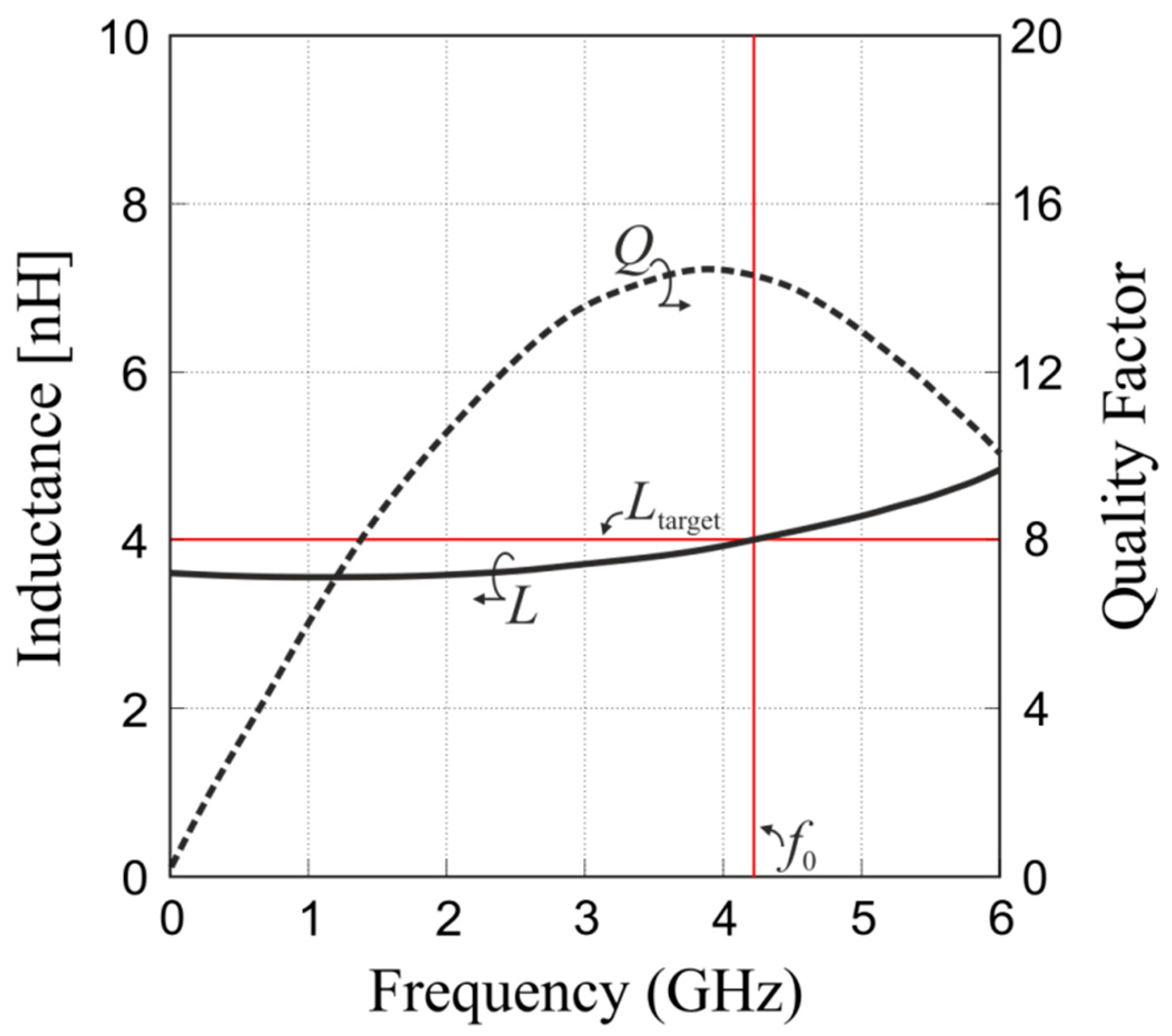
| 4 nH | 4.2 GHz | 4 nH | 14.5 | 3.85 GHz |
| x1 [μm] | x2 [μm] | x3 [μm] | |
| Lower bounds: lb | 2 | 1 | 56 |
| Upper bounds: ub | 16 | 7 | 140 |
| Initial design: x(0) | 9.0 | 4.0 | 98.0 |
| Algorithm Step | Number of Model Evaluations | Computational Cost | |
| Absolute [min] | Relative toRf | ||
| Optimization of Rc.1 | 20 × Rc.1 | 20 | 0.31 |
| Optimization of Rc.2 | 22 × Rc.2 | 55 | 0.86 |
| Setup of model q1 | 3 × 7 × Rc.2 | 53 | 0.83 |
| Evaluation of Rf | 4 × Rf | 256 | 4 |
| Total cost | n/a | 384 | 6 |
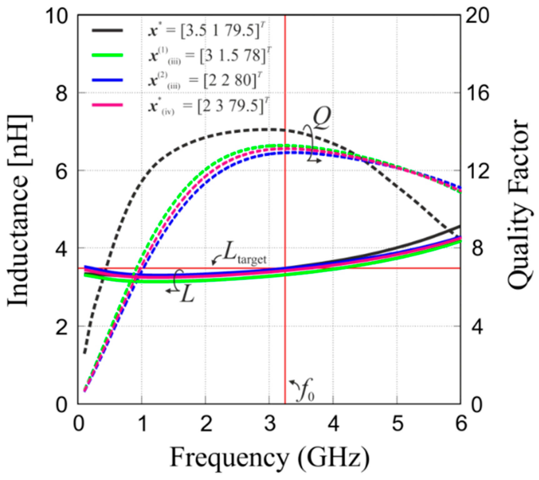
| Method | Final Design | L @ f0 | Q @ f0 | fQmax | Layout Area | CPU Cost (Relative to Rf) |
| This work | x* = [3.5 1 79.5]T | 3.49 nH | 14.1 | 3.0 GHz | 12,882 μm2 | 6 |
| Pattern search algorithm | x*(i) = [3.5 1 79.5]T | 3.49 nH | 14.1 | 3.0 GHz | 12,882 μm2 | 42 |
| Customized Enumeration 1 | x(1)(iii) = [3 1.5 78]T | 3.32 nH | 13.3 | 3.2 GHz | 12,321 μm2 | 18.78 |
| x(2)(iii) = [2 2 80]T | 3.48 nH | 12.9 | 3.37 GHz | 11,664 μm2 | 77.78 | |
| ISM with GP | x*(iv) = [2 3 79.5]T | 3.44 nH | 12.8 | 3.44 GHz | 12,882 μm2 | 8 |
| Ref. | Number of Turns | Specifications | Inductor Performance and Area | ||||
| Ltarget | f0 | Amax | L @ f0 | Q @ f0 | Layout Area | ||
| [43] | 3 1 | 3.49 nH | 3.25 GHz | – | 3.49 nH | 16.6 | 37,488 μm2 |
| [44] | 3.5 2 | 3.50 nH | 3.25 GHz | – | 3.50 nH | 16.3 | 30,002 μm2 |
| [43] | 4 1 | 3.49 nH | 3.25 GHz | – | 3.50 nH | 15.7 | 27,001 μm2 |
| This work | 4 1 | 3.49 nH | 3.25 GHz | 13,000 μm2 | 3.49 nH | 14.1 | 12,882 μm2 |
| [43] | 5 1 | 3.49 nH | 3.25 GHz | – | 3.50 nH | 12.5 | 6989 μm2 |
Publisher’s Note: MDPI stays neutral with regard to jurisdictional claims in published maps and institutional affiliations. |
© 2021 by the author. Licensee MDPI, Basel, Switzerland. This article is an open access article distributed under the terms and conditions of the Creative Commons Attribution (CC BY) license (https://creativecommons.org/licenses/by/4.0/).
Share and Cite
Kurgan, P. Efficient Surrogate Modeling and Design Optimization of Compact Integrated On-Chip Inductors Based on Multi-Fidelity EM Simulation Models. Micromachines 2021, 12, 1341. https://doi.org/10.3390/mi12111341
Kurgan P. Efficient Surrogate Modeling and Design Optimization of Compact Integrated On-Chip Inductors Based on Multi-Fidelity EM Simulation Models. Micromachines. 2021; 12(11):1341. https://doi.org/10.3390/mi12111341
Chicago/Turabian StyleKurgan, Piotr. 2021. "Efficient Surrogate Modeling and Design Optimization of Compact Integrated On-Chip Inductors Based on Multi-Fidelity EM Simulation Models" Micromachines 12, no. 11: 1341. https://doi.org/10.3390/mi12111341
APA StyleKurgan, P. (2021). Efficient Surrogate Modeling and Design Optimization of Compact Integrated On-Chip Inductors Based on Multi-Fidelity EM Simulation Models. Micromachines, 12(11), 1341. https://doi.org/10.3390/mi12111341