
Integrated Fabrication of Novel Inkjet-Printed Silver Nanoparticle Sensors on Carbon Fiber Reinforced Nylon Composites

Abstract
:
1. Introduction
2. Materials and Methods
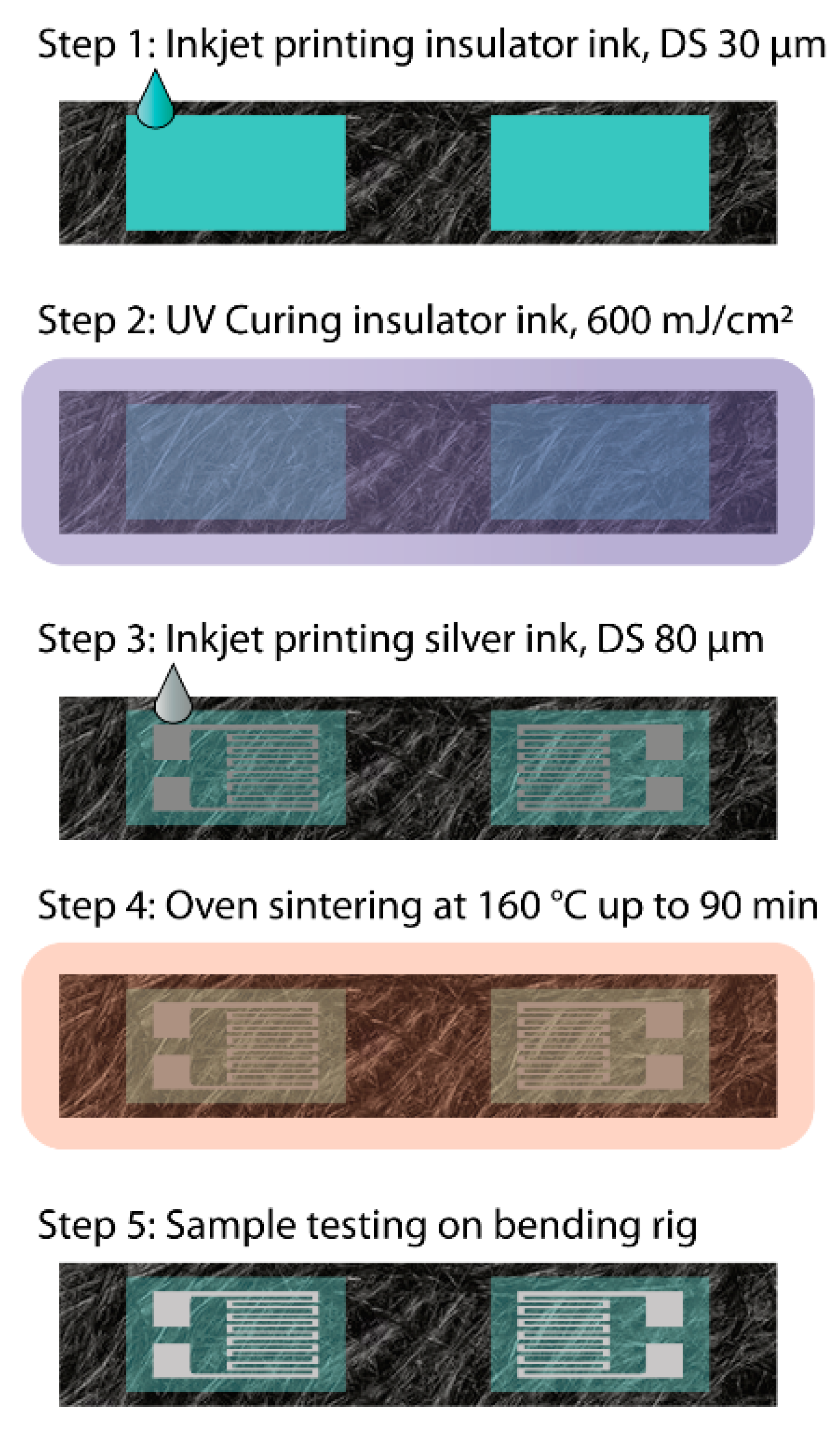
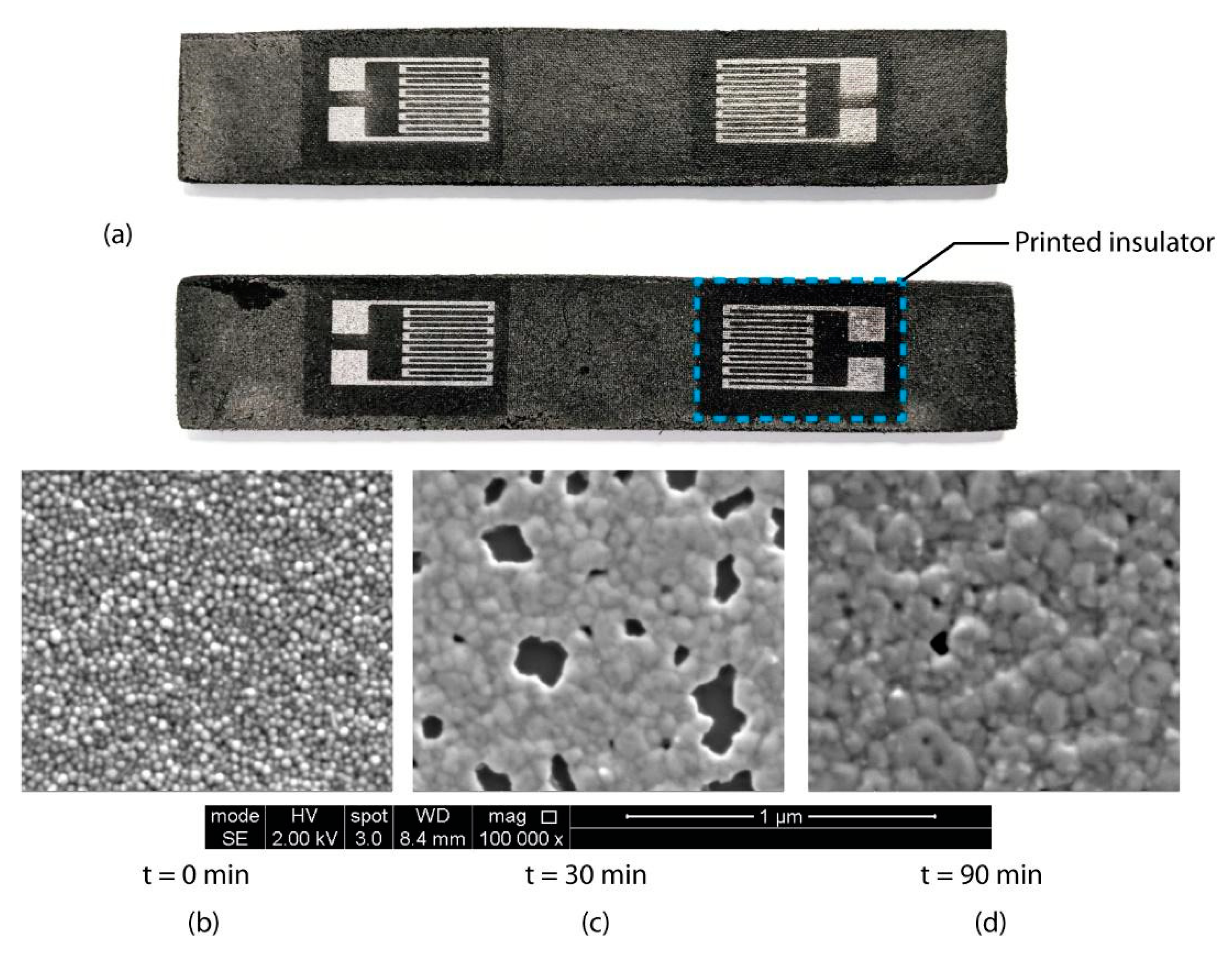
2.1. Composite Sample Fabrication
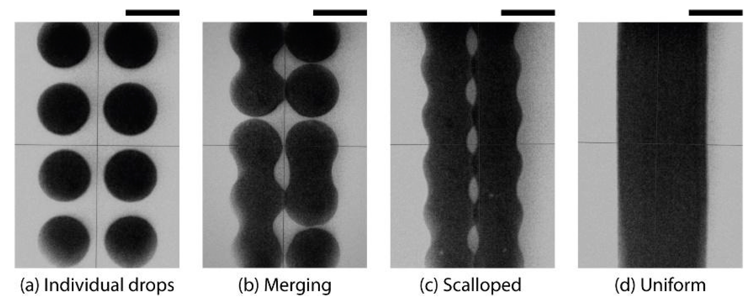
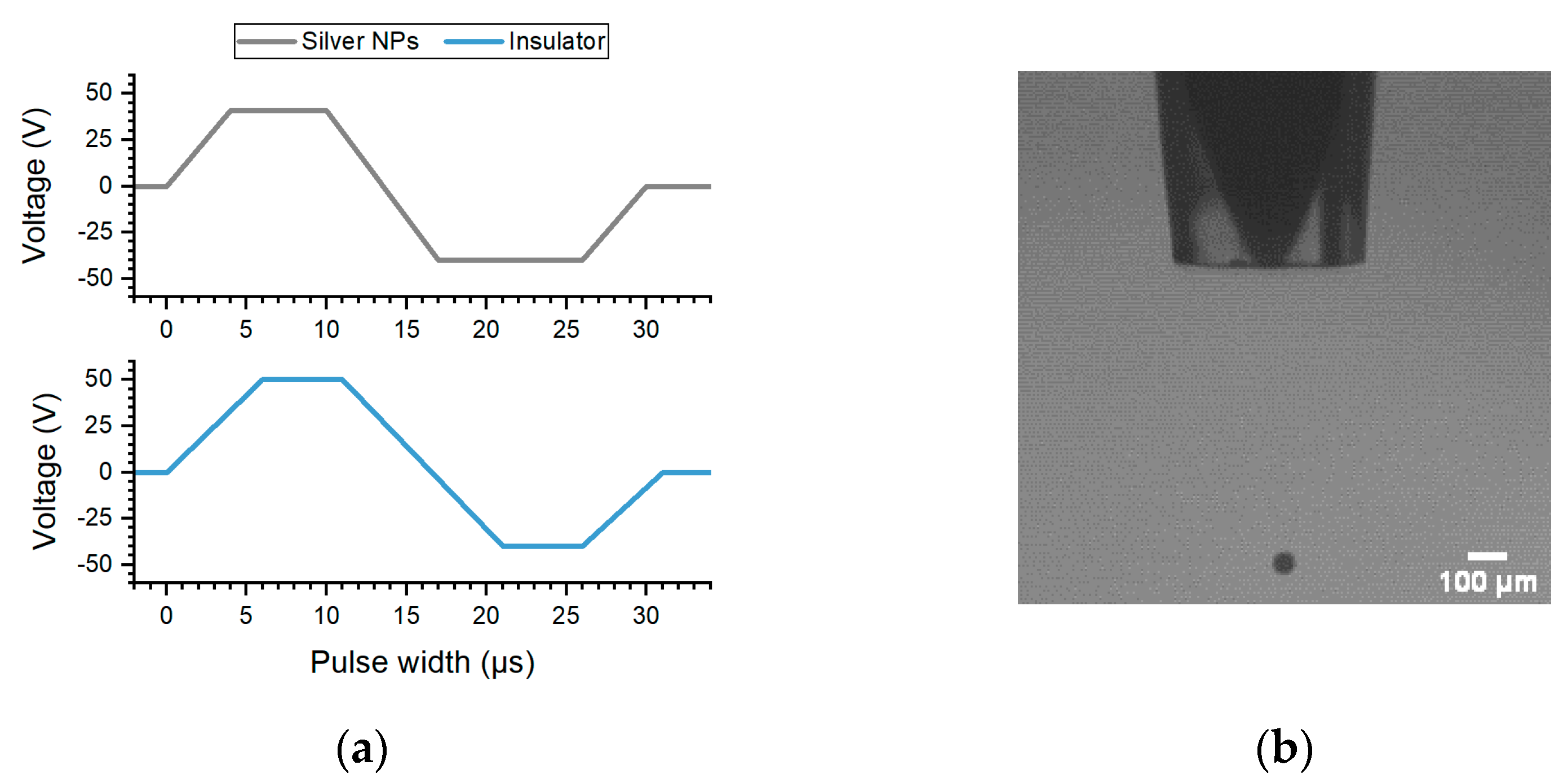
2.2. Inkjet Printing
2.3. UV Curing
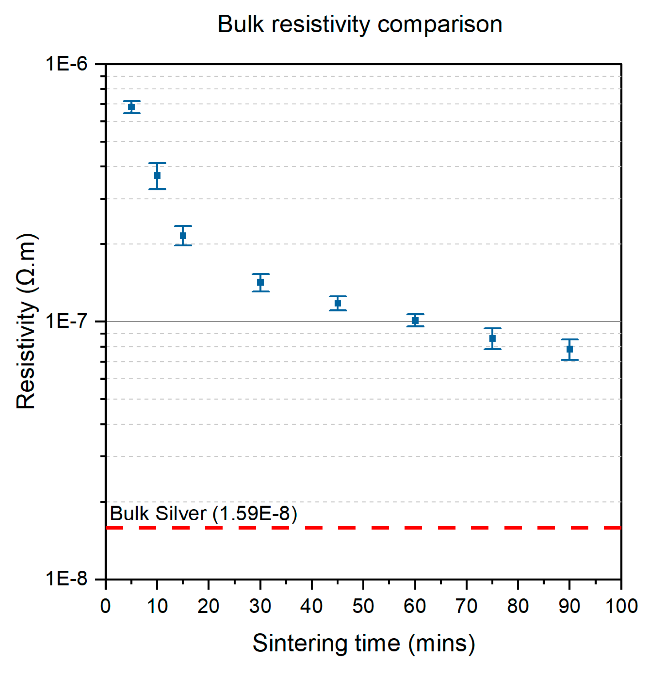
2.4. Silver Nanoparticle Sintering
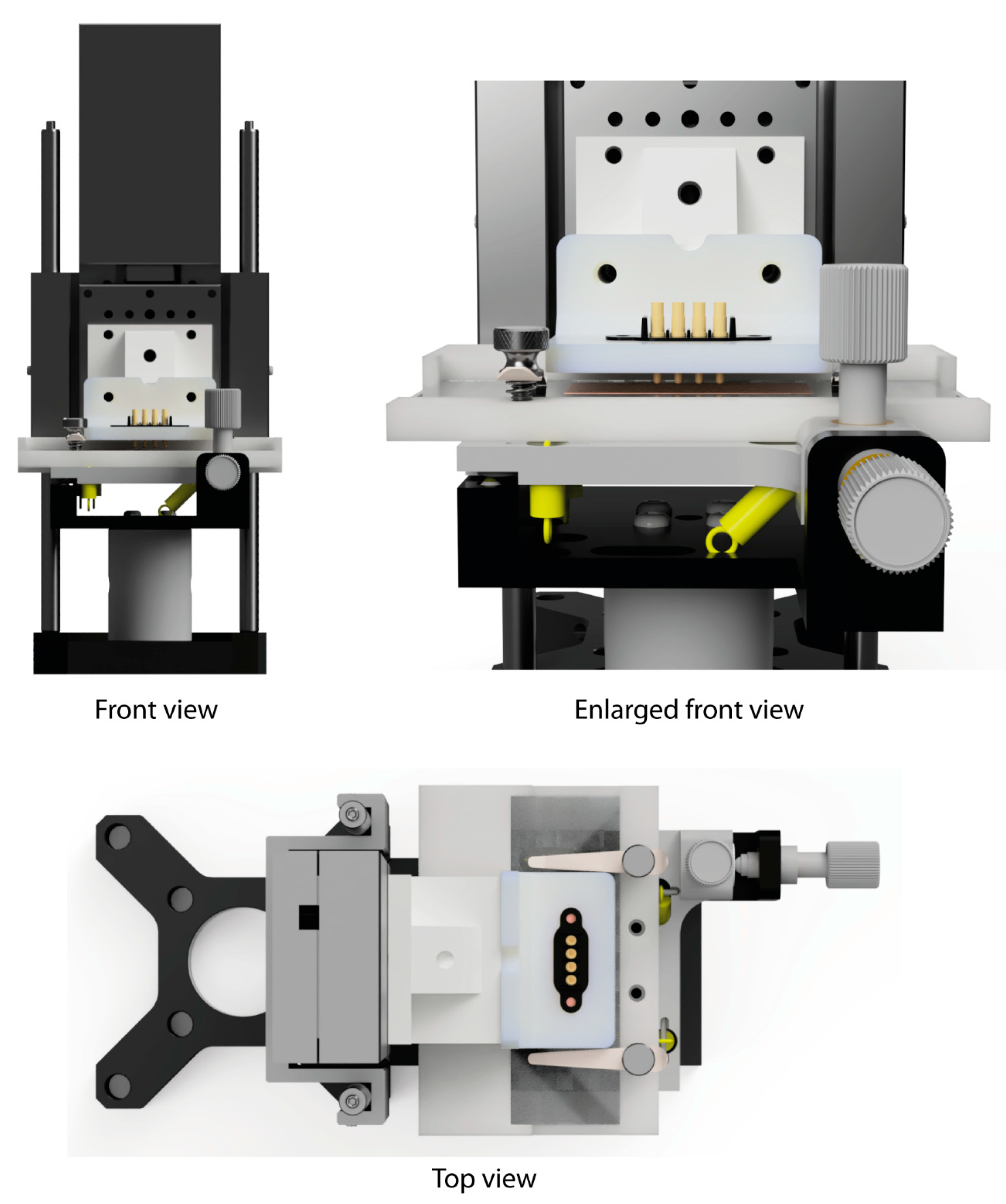
2.5. Conductivity Evaluation Using a Four-Point Probe
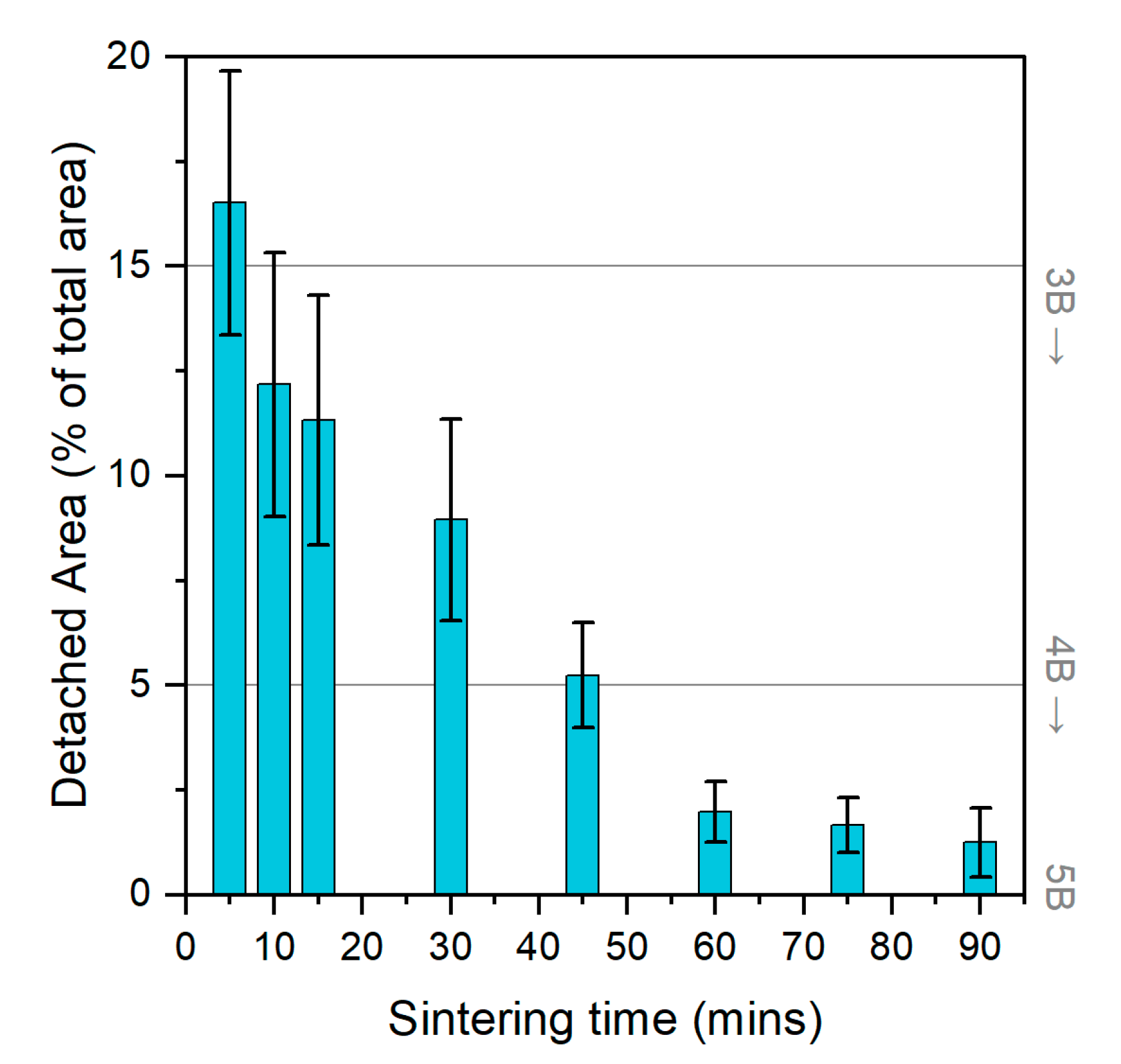
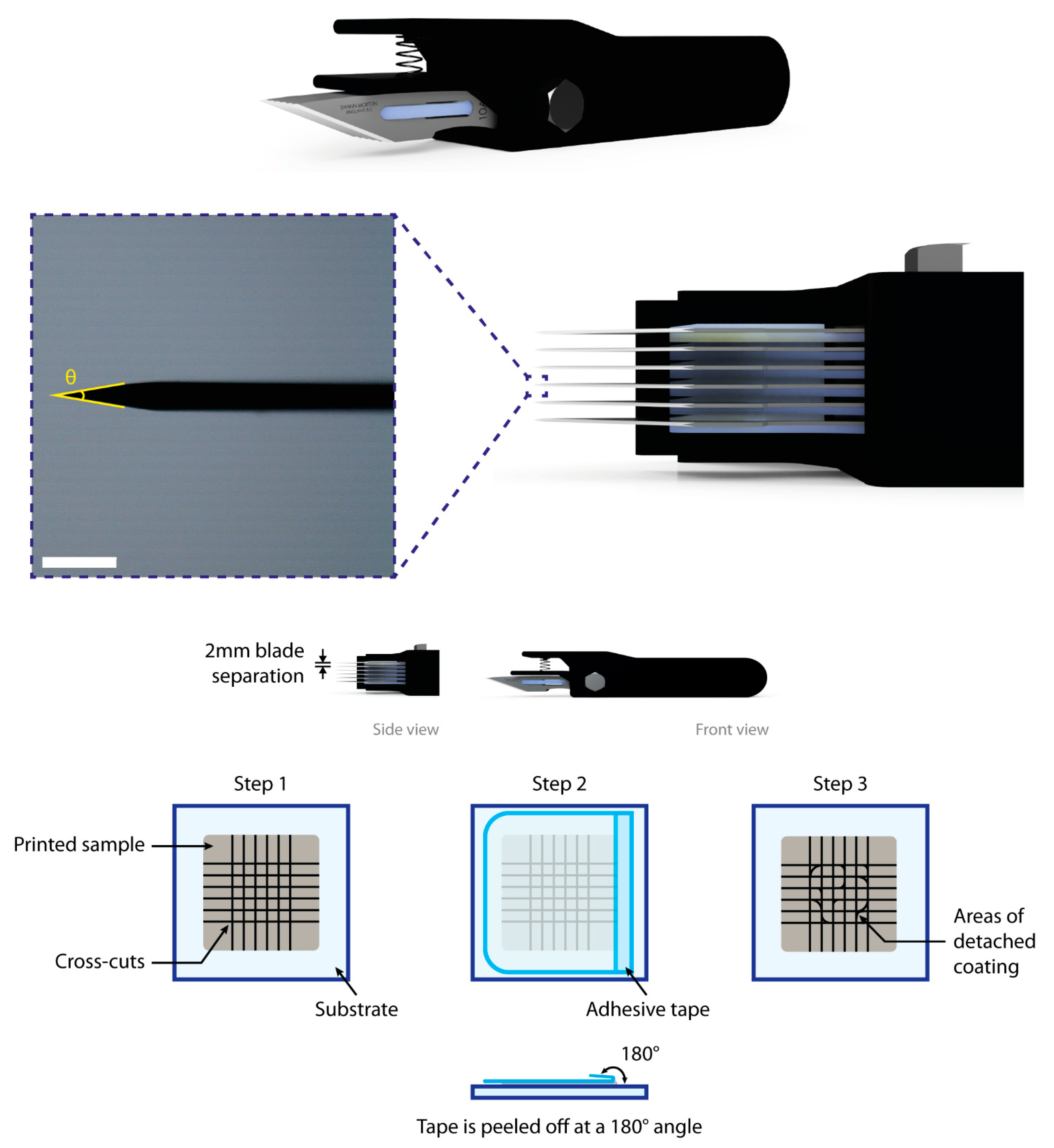
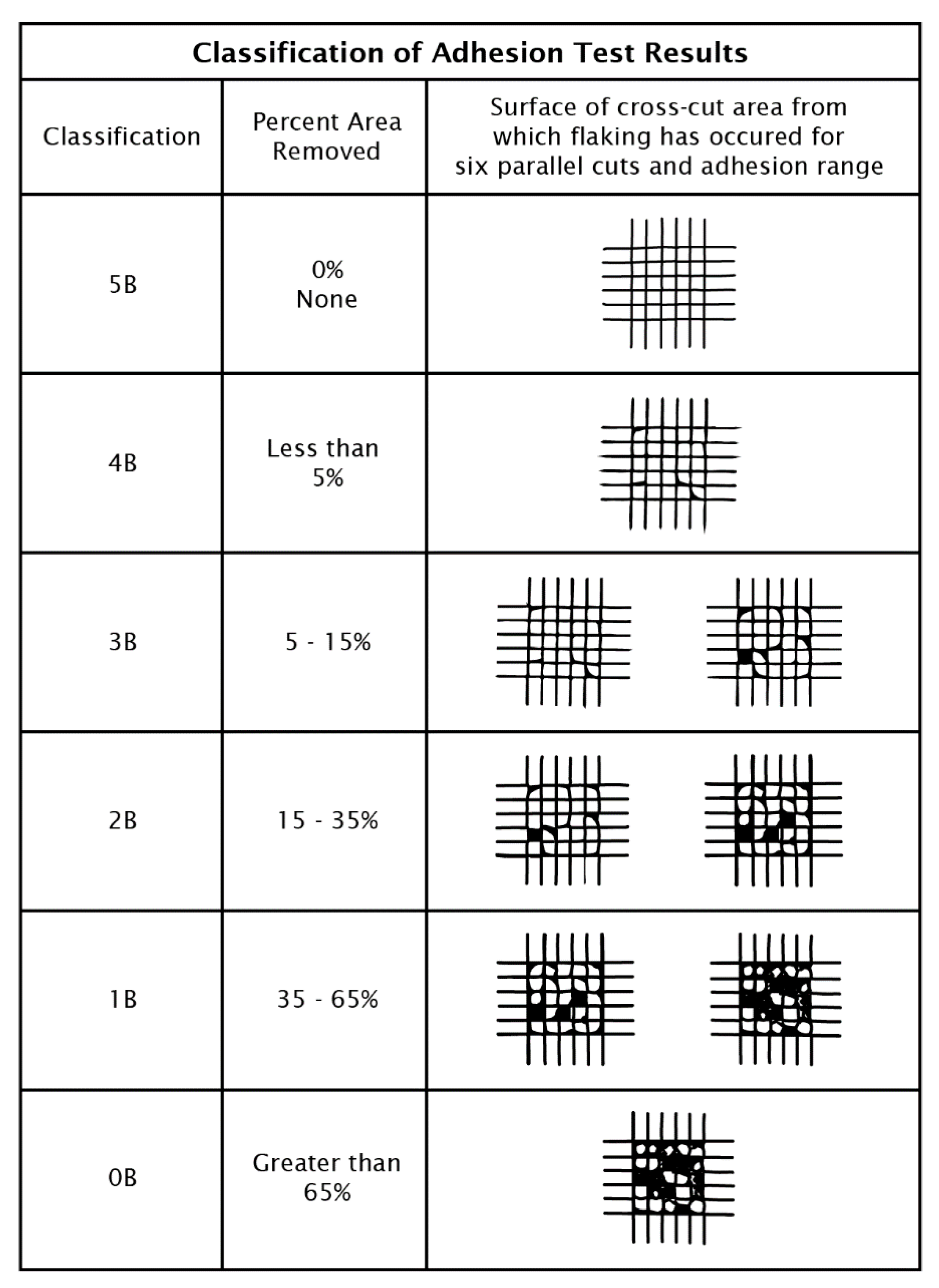
2.6. Adhesion Evaluation According to the F1842-15 Standard
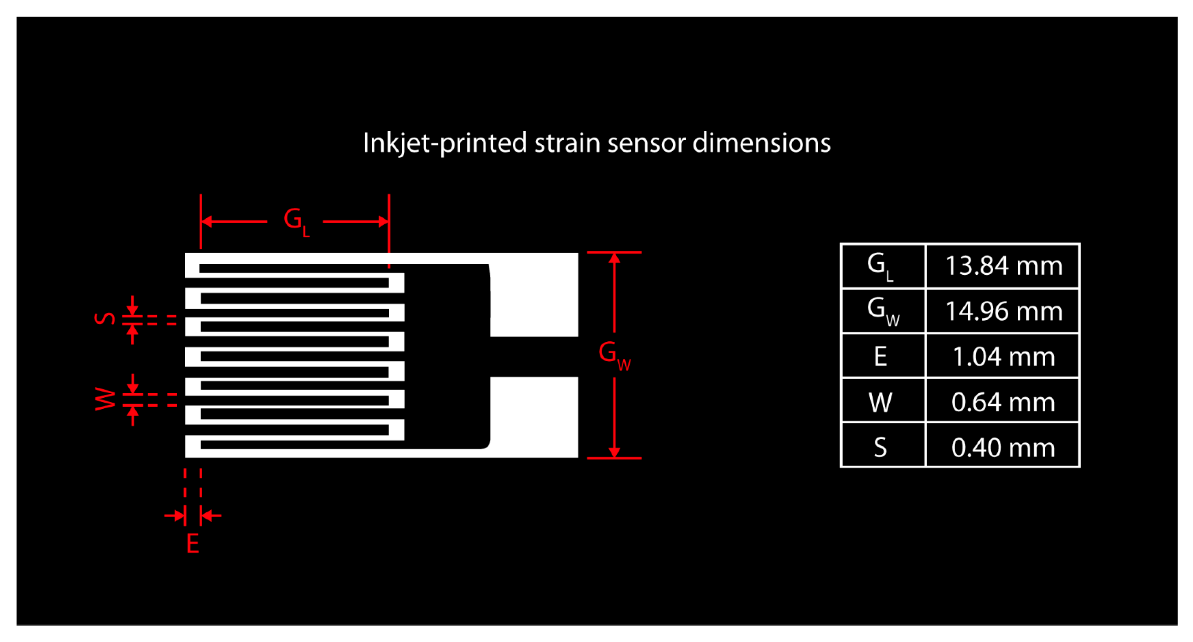
2.7. Thickness of Inkjet-Printed Samples
2.8. Sensor Performance Characterization
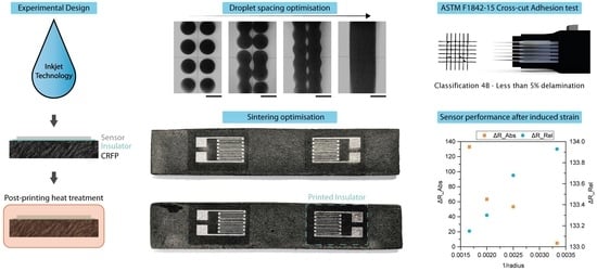
3. Results and Discussion
3.1. Conductivity Optimisation
3.2. Adhesion Classification
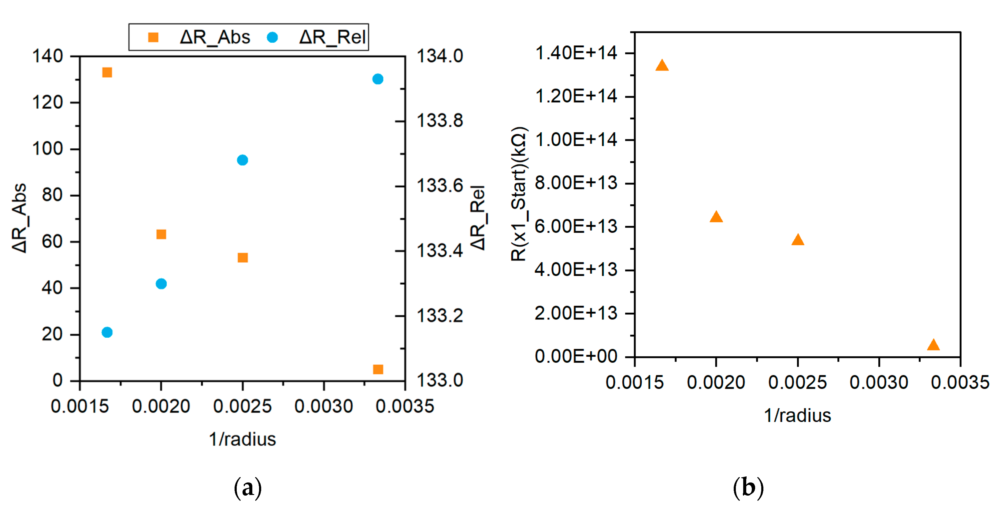
3.3. Sensor Performance after Induced Strain
- The sensors should monitor the real-time structural performance of the structure and be immune to external factors;
- The signal transmission from the sensor to the data acquisition device should be reliable;
- The embedment of the sensor should not be detrimental to the performance of the structure;
- The lifespan of the sensors should be parallel to the lifespan of the structure;
- The sensors should be easily commissioned on the structure, including minimizing the risk of delamination.
4. Conclusions
Author Contributions
Funding
Data Availability Statement
Acknowledgments
Conflicts of Interest
Appendix A

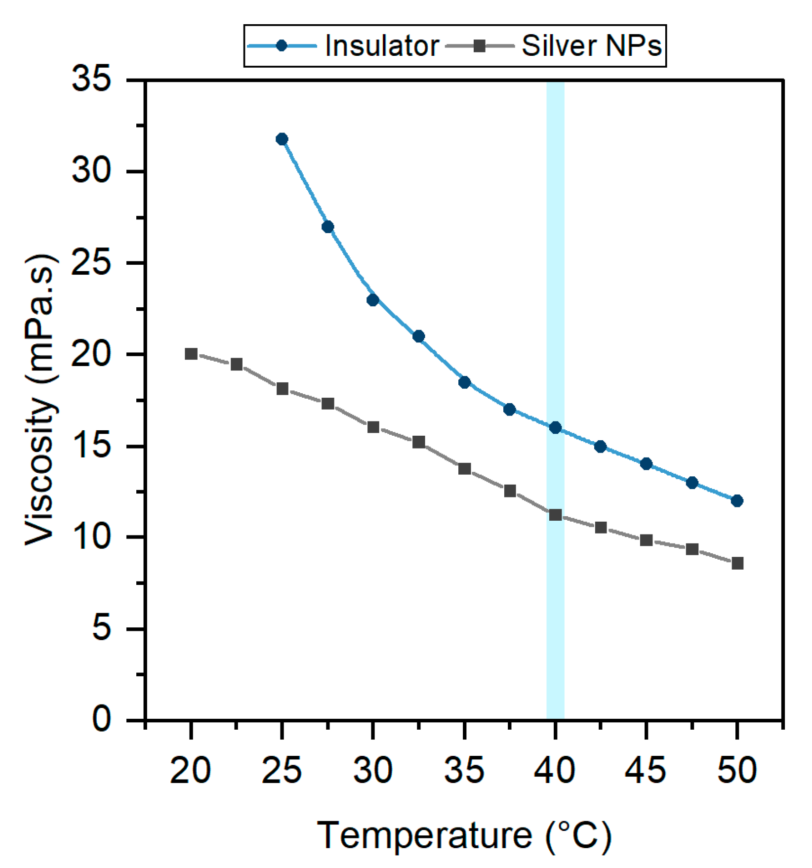
| Ink | Viscosity (cP) | Particle Content wt. % | Recommended Sintering Temp. | Recommended Sintering Time | Manufacturer |
|---|---|---|---|---|---|
| INI | 16.00 at 40 °C | - | - * UV | - * UV | Dycotec Materials (DM-INI-7003) |
| AgNPs | 11.25 at 40 °C | 30–35 | 150 °C | 30 min | Sigma-Aldrich (no. 736465) |

Appendix B
Appendix C
Appendix D
Appendix E

References
- Martin, G.D.; Hoath, S.D.; Hutchings, I.M. Inkjet printing—The physics of manipulating liquid jets and drops. J. Phys. Conf. Ser. 2008, 105, 012001. [Google Scholar] [CrossRef] [Green Version]
- Tekin, E.; Smith, P.J.; Schubert, U.S. Inkjet printing as a deposition and patterning tool for polymers and inorganic particles. Soft Matter 2008, 4, 703–713. [Google Scholar] [CrossRef] [PubMed]
- de Gans, B.-J.; Schubert, U.S. Inkjet Printing of Well-Defined Polymer Dots and Arrays. Langmuir 2004, 20, 7789–7793. [Google Scholar] [CrossRef] [PubMed]
- De Gans, B.J.; Duineveld, P.C.; Schubert, U.S. Inkjet printing of polymers: State of the art and future developments. Adv. Mater. 2004, 16, 203–213. [Google Scholar] [CrossRef]
- Derby, B. Inkjet printing ceramics: From drops to solid. J. Eur. Ceram. Soc. 2011, 31, 2543–2550. [Google Scholar] [CrossRef]
- Derby, B. Additive Manufacture of Ceramics Components by Inkjet Printing. Engineering 2015, 1, 113–123. [Google Scholar] [CrossRef] [Green Version]
- Boland, T.; Xu, T.; Damon, B.; Cui, X. Application of inkjet printing to tissue engineering. Biotechnol. J. 2006, 1, 910–917. [Google Scholar] [CrossRef]
- Xu, T.; Jin, J.; Gregory, C.; Hickman, J.J.; Boland, T. Inkjet printing of viable mammalian cells. Biomaterials 2005, 26, 93–99. [Google Scholar] [CrossRef]
- Torrisi, F.; Hasan, T.; Wu, W.; Sun, Z.; Lombardo, A.; Kulmala, T.S.; Hsieh, G.W.; Jung, S.; Bonaccorso, F.; Paul, P.J.; et al. Inkjet-printed graphene electronics. ACS Nano 2012, 6, 2992–3006. [Google Scholar] [CrossRef]
- Beedasy, V.; Smith, P.J. Printed electronics as prepared by inkjet printing. Materials 2020, 13, 704. [Google Scholar] [CrossRef] [Green Version]
- Niittynen, J.; Sowade, E.; Kang, H.; Baumann, R.R.; M??ntysalo, M.; Mäntysalo, M.; Sowade, E.; Niittynen, J.; Kang, H.; Sowade, E.; et al. Comparison of laser and intense pulsed light sintering (IPL) for inkjet-printed copper nanoparticle layers. Sci. Rep. 2015, 5, 8832. [Google Scholar] [CrossRef] [PubMed]
- Chan, H.J.; Huang, B.C.; Wang, L.W.; Liao, K.H.; Lo, C.Y. Porosity reduction in inkjet-printed copper film by progressive sintering on nanoparticles. Thin Solid Films 2017, 627, 33–38. [Google Scholar] [CrossRef]
- Huang, D.; Liao, F.; Molesa, S.; Redinger, D.; Subramanian, V. Plastic-compatible low resistance printable gold nanoparticle conductors for flexible electronics. J. Electrochem. Soc. 2003, 150, G412. [Google Scholar] [CrossRef] [Green Version]
- Perelaer, J.; Smith, P.J.; Mager, D.; Soltman, D.; Volkman, S.K.; Subramanian, V.; Korvink, J.G.; Schubert, U.S. Printed electronics: The challenges involved in printing devices, interconnects, and contacts based on inorganic materials. J. Mater. Chem. 2010, 20, 8446. [Google Scholar] [CrossRef]
- Magdassi, S.; Grouchko, M.; Berezin, O.; Kamyshny, A. Triggering the sintering of silver nanoparticles at room temperature. ACS Nano 2010, 4, 1943–1948. [Google Scholar] [CrossRef]
- Black, K.; Singh, J.; Mehta, D.; Sung, S.; Sutcliffe, C.J.; Chalker, P.R. Silver ink formulations for sinter-free printing of conductive films. Sci. Rep. 2016, 6, 20814. [Google Scholar] [CrossRef] [Green Version]
- Smith, P.J.; Shin, D.Y.; Stringer, J.E.; Derby, B.; Reis, N. Direct ink-jet printing and low temperature conversion of conductive silver patterns. J. Mater. Sci. 2006, 41, 4153–4158. [Google Scholar] [CrossRef]
- Wilson, C.L.; Lonkar, K.; Roy, S.; Kopsaftopoulos, F.; Chang, F.K. Structural health monitoring of composites. In Comprehensive Composite Materials II; Elsevier: Amsterdam, The Netherlands, 2017; pp. 382–407. ISBN 9780081005330. [Google Scholar]
- López-Higuera, J.M.; Cobo, L.R.; Incera, A.Q.; Cobo, A. Fiber optic sensors in structural health monitoring. J. Light. Technol. 2011, 29, 587–608. [Google Scholar] [CrossRef]
- Maheshwari, M.; Annamdas, V.G.M.; Pang, J.H.L.; Asundi, A.; Tjin, S.C. Crack monitoring using multiple smart materials; fiber-optic sensors & piezo sensors. Int. J. Smart Nano Mater. 2017, 8, 41–55. [Google Scholar]
- Giurgiutiu, V. Structural Health Monitoring of Aerospace Composites; Elsevier Inc.: Amsterdam, The Netherlands, 2015; ISBN 9780124104419. [Google Scholar]
- Herszberg, I.; Bannister, M.K.; Li, H.C.H.; Thomson, R.S.; White, C. Structural health monitoring for advanced composite structures. ICCM Int. Conf. Compos. Mater. 2007, 4, 13. [Google Scholar]
- Zhou, G.; Sim, L.M. Damage detection and assessment in fibre-reinforced composite structures with embedded fibre optic sensors-review. Smart Mater. Struct. 2002, 11, 925–939. [Google Scholar] [CrossRef]
- Kang, I.; Schulz, M.J.; Kim, J.H.; Shanov, V.; Shi, D. A carbon nanotube strain sensor for structural health monitoring. Smart Mater. Struct. 2006, 15, 737–748. [Google Scholar] [CrossRef]
- Sun, M.Q.; Liew, R.J.Y.; Zhang, M.H.; Li, W. Development of cement-based strain sensor for health monitoring of ultra high strength concrete. Constr. Build. Mater. 2014, 65, 630–637. [Google Scholar] [CrossRef]
- Cochrane, C.; Lewandowski, M.; Koncar, A.V. A flexible strain sensor based on a conductive polymer composite for in situ measurement of parachute canopy deformation. Sensors 2010, 10, 8291–8303. [Google Scholar] [CrossRef] [PubMed] [Green Version]
- Rocha, H.; Semprimoschnig, C.; Nunes, J.P. Sensors for process and structural health monitoring of aerospace composites: A review. Eng. Struct. 2021, 237, 112231. [Google Scholar] [CrossRef]
- Swartz, R.; Gore, E.; Crist, B.; Bayldon, J.; Wagner, C.; Tarzian, N.; Su, E. Wo2017139766—Method and Apparatus for Automated Composite-Based Additive Manufacturing. U.S. Patent 10046552, 17 August 2017. [Google Scholar]
- International, A. Standard Test Methods for Measuring Adhesion by Tape Test. Annu. B. ASTM Stand. 2013, 6, 1–7. [Google Scholar]
- Lukacs, P.; Pietrikova, A.; Kovac, O. Improvement of the evaluation of inkjet printed silver based layers’ adhesion. J. Adhes. Sci. Technol. 2019, 33, 124–136. [Google Scholar] [CrossRef]
- ASTM Standards. Standard Test Method for Determining Ink or Coating Adhesion on Flexible Substrates for a Membrane Switch or Printed Electronic Device; ASTM: West Conshohocken, CA, USA, 2015. [Google Scholar]
- Huang, L.; Lv, X.; Tang, Y.; Ge, G.; Zhang, P.; Li, Y. Effect of alumina nanowires on the thermal conductivity and electrical performance of epoxy composites. Polymers 2020, 12, 2126. [Google Scholar] [CrossRef] [PubMed]
- Yang, Z.; Wang, Q. A simple approach to measure the surface resistivity of insulating materials. In Proceedings of the IECON Proceedings (Industrial Electronics Conference), Melbourne, VIC, Australia, 7–11 November 2011; pp. 2088–2093. [Google Scholar]
- Borghetti, M.; Serpelloni, M.; Sardini, E. Printed strain gauge on 3D and low-melting point plastic surface by aerosol jet printing and photonic curing. Sensors 2019, 19, 4220. [Google Scholar] [CrossRef] [Green Version]
- Martinez, V.; Stauffer, F.; Adagunodo, M.O.; Forro, C.; Vörös, J.; Larmagnac, A. Stretchable Silver Nanowire-Elastomer Composite Microelectrodes with Tailored Electrical Properties. ACS Appl. Mater. Interfaces 2015, 7, 13467–13475. [Google Scholar] [CrossRef]
- Su, Z.; Wu, H.; Chen, H.; Guo, H.; Cheng, X.; Song, Y.; Chen, X.; Zhang, H. Digitalized self-powered strain gauge for static and dynamic measurement. Nano Energy 2017, 42, 129–137. [Google Scholar] [CrossRef]
- Triethylene Glycol Monomethyl Ether 95%, 112-35-6; Sigma Aldrich: St Louis, MO, USA, 2019.
- Voorhees, P.W. The theory of Ostwald ripening. J. Stat. Phys. 1985, 38, 231–252. [Google Scholar] [CrossRef] [Green Version]
- Greer, J.R.; Street, R.A. Thermal cure effects on electrical performance of nanoparticle silver inks. Acta Mater. 2007, 55, 6345–6349. [Google Scholar] [CrossRef]
- Siegel, J.; Lyutakov, O.; Rybka, V.; Kolská, Z.; Švorčík, V. Properties of gold nanostructures sputtered on glass. Nanoscale Res. Lett. 2011, 6, 1–19. [Google Scholar] [CrossRef] [Green Version]
- Larsson, M.P.; Ahmad, M.M. Improved polymer-glass adhesion through micro-mechanical interlocking. J. Micromech. Microeng. 2006, 16, 161–168. [Google Scholar] [CrossRef]
- Halonen, E.; Viiru, T.; Östman, K.; Cabezas, A.L.; Mantysalo, M. Oven sintering process optimization for inkjet-printed Ag Nanoparticle ink. IEEE Trans. Components Packag. Manuf. Technol. 2013, 3, 350–356. [Google Scholar] [CrossRef]
- Niittynen, J.; Abbel, R.; Mäntysalo, M.; Perelaer, J.; Schubert, U.S.; Lupo, D. Alternative sintering methods compared to conventional thermal sintering for inkjet printed silver nanoparticle ink. Thin Solid Films 2014, 556, 452–459. [Google Scholar] [CrossRef]
- Kirtania, S.G.; Riheen, M.A.; Kim, S.U.; Sekhar, K.; Wisniewska, A.; Sekhar, P.K. Inkjet printing on a new flexible ceramic substrate for Internet of Things (IoT) applications. Micromachines 2020, 11, 841. [Google Scholar] [CrossRef]
- Komurlu, E.; Cihangir, F.; Kesimal, A.; Demir, S. Effect of Adhesive Type on the Measurement of Modulus of Elasticity Using Electrical Resistance Strain Gauges. Arab. J. Sci. Eng. 2016, 41, 433–441. [Google Scholar] [CrossRef]
- Subrahmanya, K.; Vadivuchezhian, K.; Chockappan, N. Experimental Verification of Effect of Adhesive Layer Thickness Used for Strain Gauge Mounting. Adv. Mater. Res. 2015, 1119, 789–793. [Google Scholar] [CrossRef]
- Fu, R.; Warnakula, T.; Shi, Q.; Yap, L.W.; Dong, D.; Liu, Y.; Premaratne, M.; Cheng, W. Plasmene nanosheets as optical skin strain sensors. Nanoscale Horizons 2020, 5, 1515–1523. [Google Scholar] [CrossRef] [PubMed]
- Strong, A.B. Fundamentals of composites manufacturing: Materials, methods and applications. In Composites Manufacturing; SME: Southfield, MI, USA, 2008; Volume 2, p. 166. [Google Scholar]
- Correia, V.; Caparros, C.; Casellas, C.; Francesch, L.; Rocha, J.G.; Lanceros-Mendez, S. Development of inkjet printed strain sensors. Smart Mater. Struct. 2013, 22. [Google Scholar] [CrossRef]
- Leong, Z.; Holmes, W.; Clarke, J.; Padki, A.; Hayes, S.; Morley, N.A. Magnetostrictive Sensors for Composite Damage Detection and Wireless Structural Health Monitoring. IEEE Trans. Magn. 2019, 55, 105028. [Google Scholar] [CrossRef]
- Gullapalli, A.; Beedasy, V.; Vincent, J.D.S.; Leong, Z.; Smith, P.; Morley, N. Flat Inkjet-Printed Copper Induction Coils for Magnetostrictive Structural Health Monitoring: A Comparison with Bulk Air Coils and an AMR Sensor. Adv. Eng. Mater. 2021, 2100313, 1–9. [Google Scholar]
- Ali, S.; Khan, S.; Bermak, A. Inkjet-Printed Human Body Temperature Sensor for Wearable Electronics. IEEE Access 2019, 7, 163981–163987. [Google Scholar] [CrossRef]
- Tuloup, C.; Harizi, W.; Aboura, Z.; Meyer, Y.; Khellil, K.; Lachat, R. On the use of in-situ piezoelectric sensors for the manufacturing and structural health monitoring of polymer-matrix composites: A literature review. Compos. Struct. 2019, 215, 127–149. [Google Scholar] [CrossRef]


Publisher’s Note: MDPI stays neutral with regard to jurisdictional claims in published maps and institutional affiliations. |
© 2021 by the authors. Licensee MDPI, Basel, Switzerland. This article is an open access article distributed under the terms and conditions of the Creative Commons Attribution (CC BY) license (https://creativecommons.org/licenses/by/4.0/).
Share and Cite
Karaş, B.; Beedasy, V.; Leong, Z.; Morley, N.A.; Mumtaz, K.; Smith, P.J. Integrated Fabrication of Novel Inkjet-Printed Silver Nanoparticle Sensors on Carbon Fiber Reinforced Nylon Composites. Micromachines 2021, 12, 1185. https://doi.org/10.3390/mi12101185
Karaş B, Beedasy V, Leong Z, Morley NA, Mumtaz K, Smith PJ. Integrated Fabrication of Novel Inkjet-Printed Silver Nanoparticle Sensors on Carbon Fiber Reinforced Nylon Composites. Micromachines. 2021; 12(10):1185. https://doi.org/10.3390/mi12101185
Chicago/Turabian StyleKaraş, Büşra, Vimanyu Beedasy, Zhaoyuan Leong, Nicola A. Morley, Kamran Mumtaz, and Patrick J. Smith. 2021. "Integrated Fabrication of Novel Inkjet-Printed Silver Nanoparticle Sensors on Carbon Fiber Reinforced Nylon Composites" Micromachines 12, no. 10: 1185. https://doi.org/10.3390/mi12101185
APA StyleKaraş, B., Beedasy, V., Leong, Z., Morley, N. A., Mumtaz, K., & Smith, P. J. (2021). Integrated Fabrication of Novel Inkjet-Printed Silver Nanoparticle Sensors on Carbon Fiber Reinforced Nylon Composites. Micromachines, 12(10), 1185. https://doi.org/10.3390/mi12101185