Exploring a New Adaptive Routing Based on the Dijkstra Algorithm in Optical Networks-on-Chip


Abstract
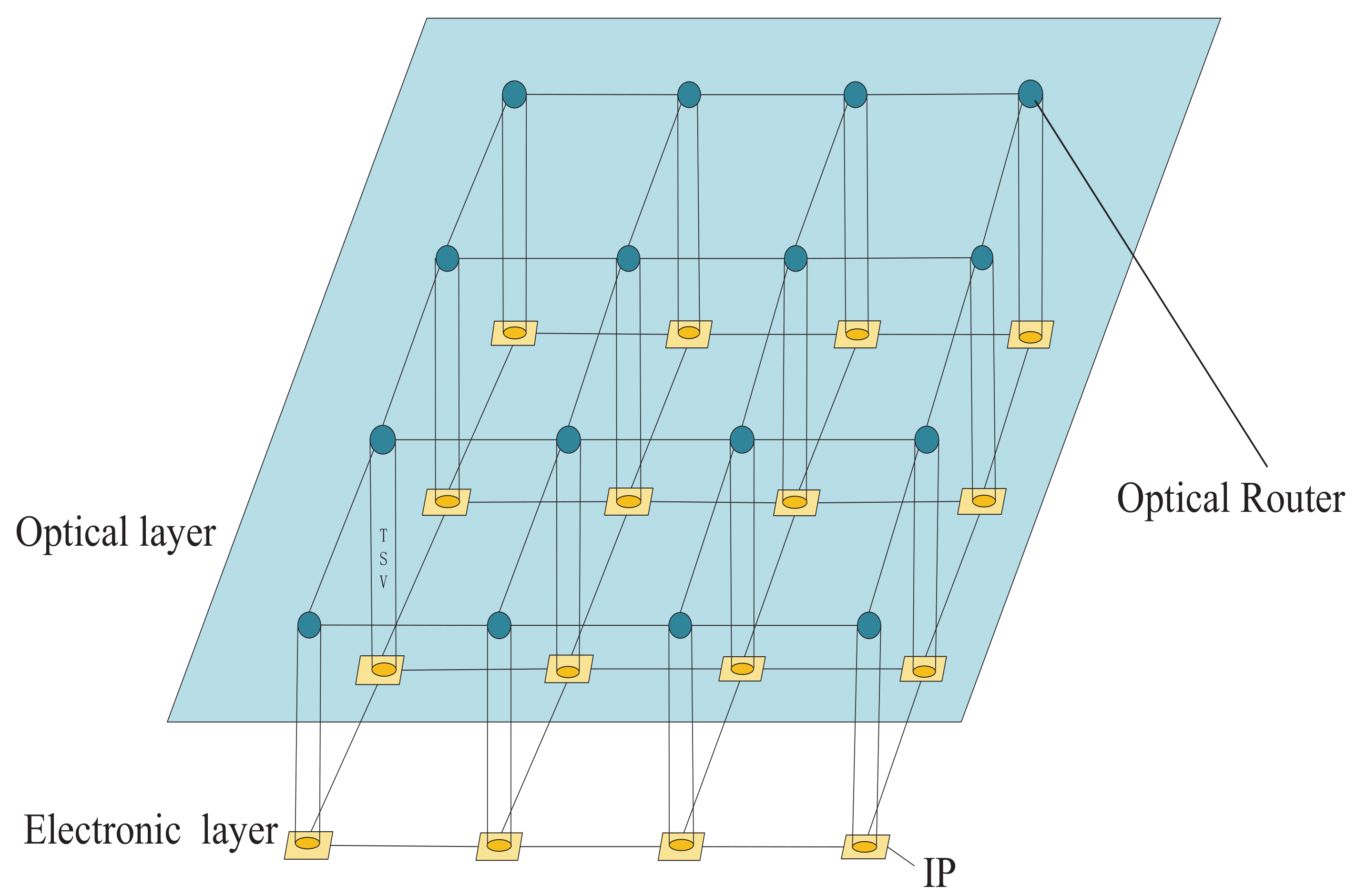
1. Introduction
2. Internal Insertion Loss Analysis of ONoCs
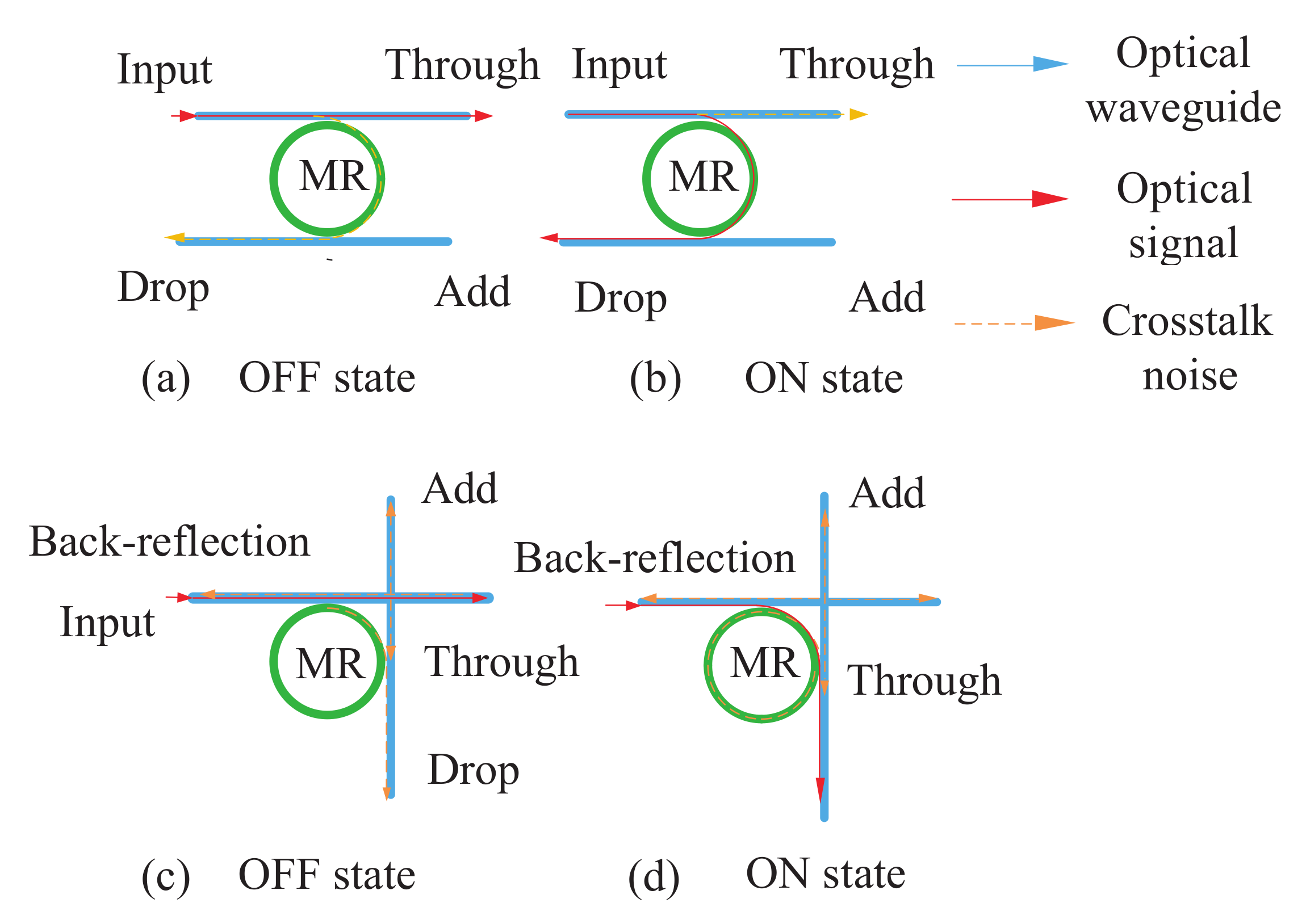
2.1. Basic Optical Switching Elements (BOSEs)
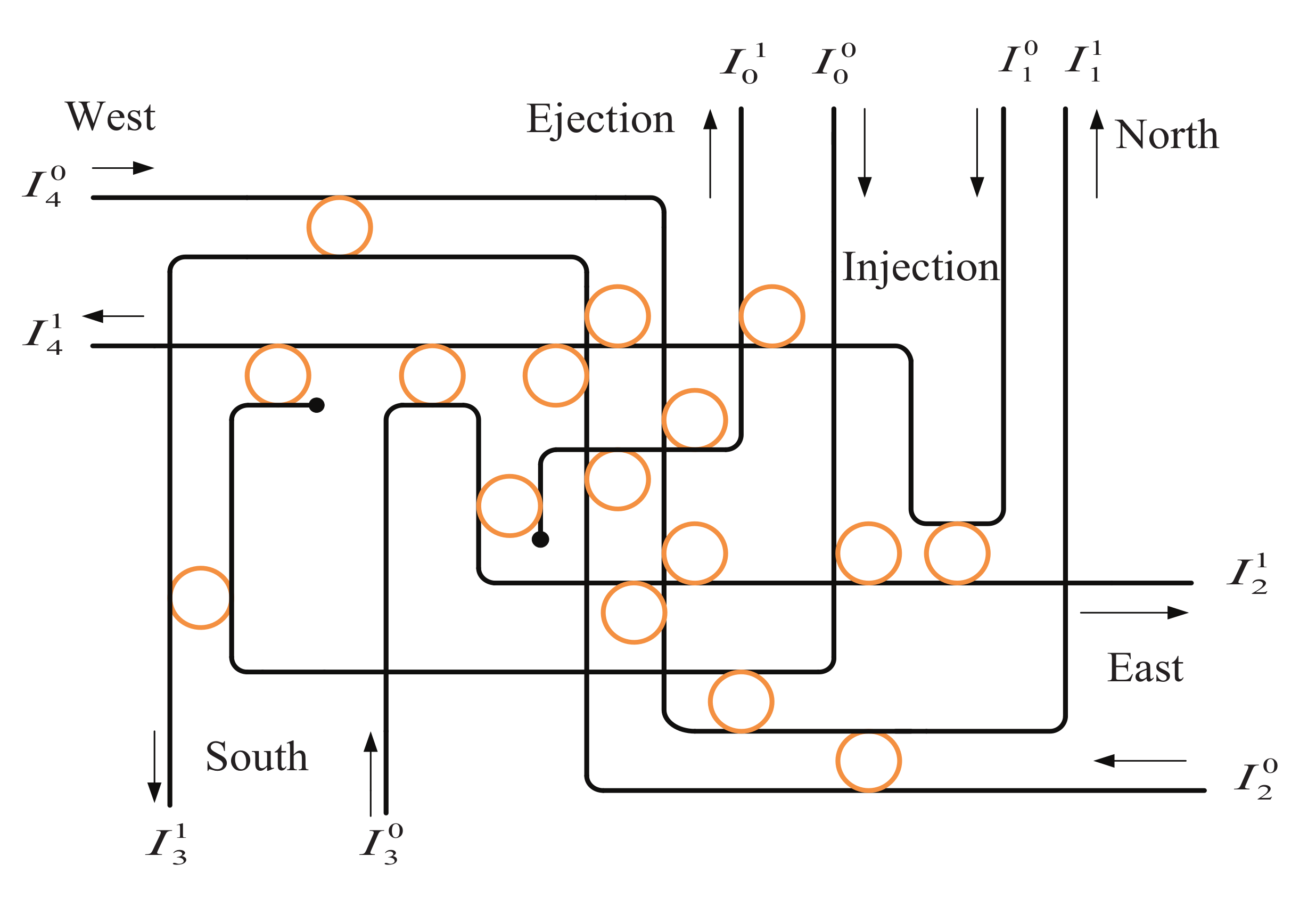
2.2. Five-Port Non-Blocking Router Model
2.3. Adaptive Power Control Model
3. Adaptive Power Control of ONoCs Based on the Dijkstra Algorithm
3.1. The Dijkstra Algorithm’s Principles
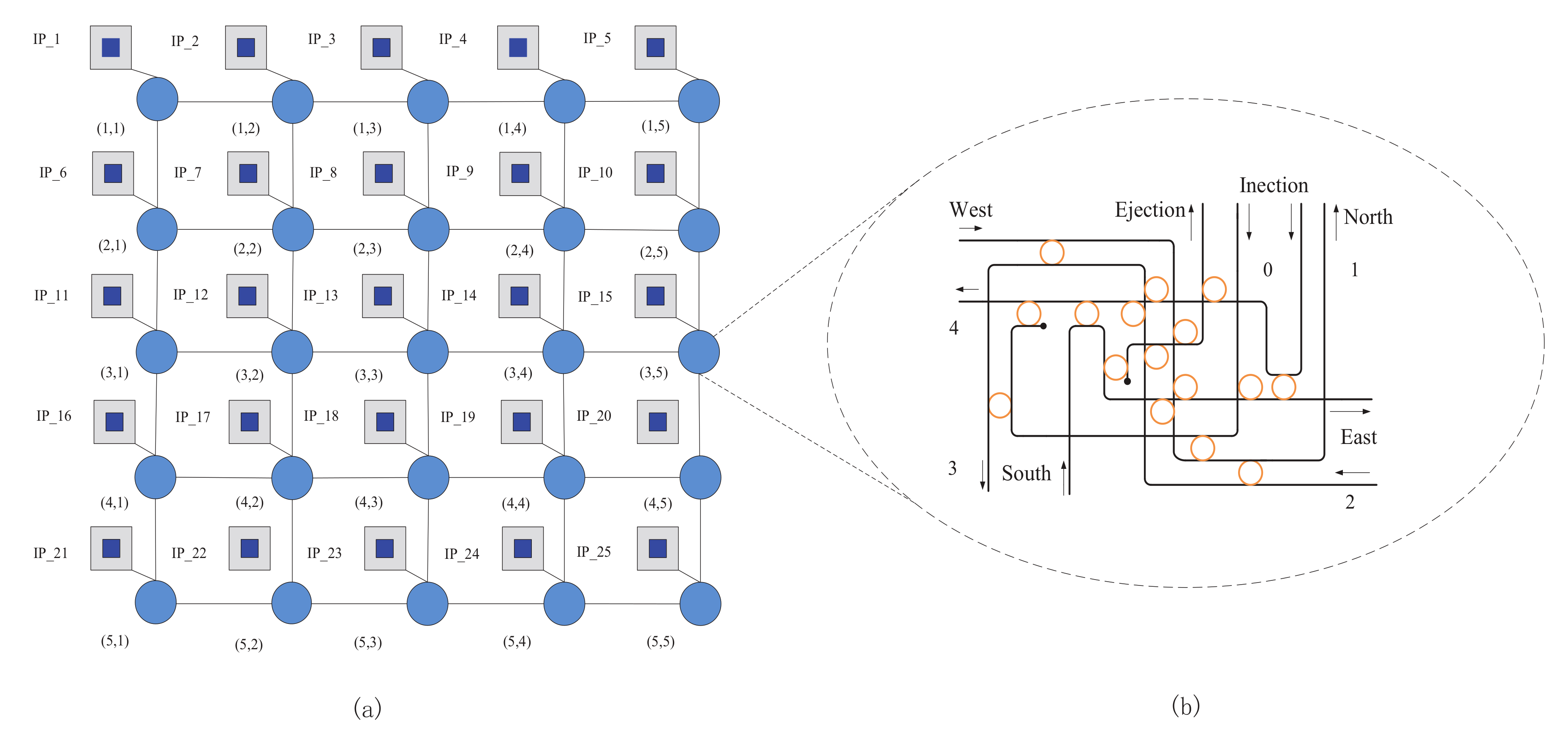
3.2. Network Architecture
| Algorithm 1: Routing algorithm based on the Dijkstra algorithm |
 |
4. Evaluation and Discussion
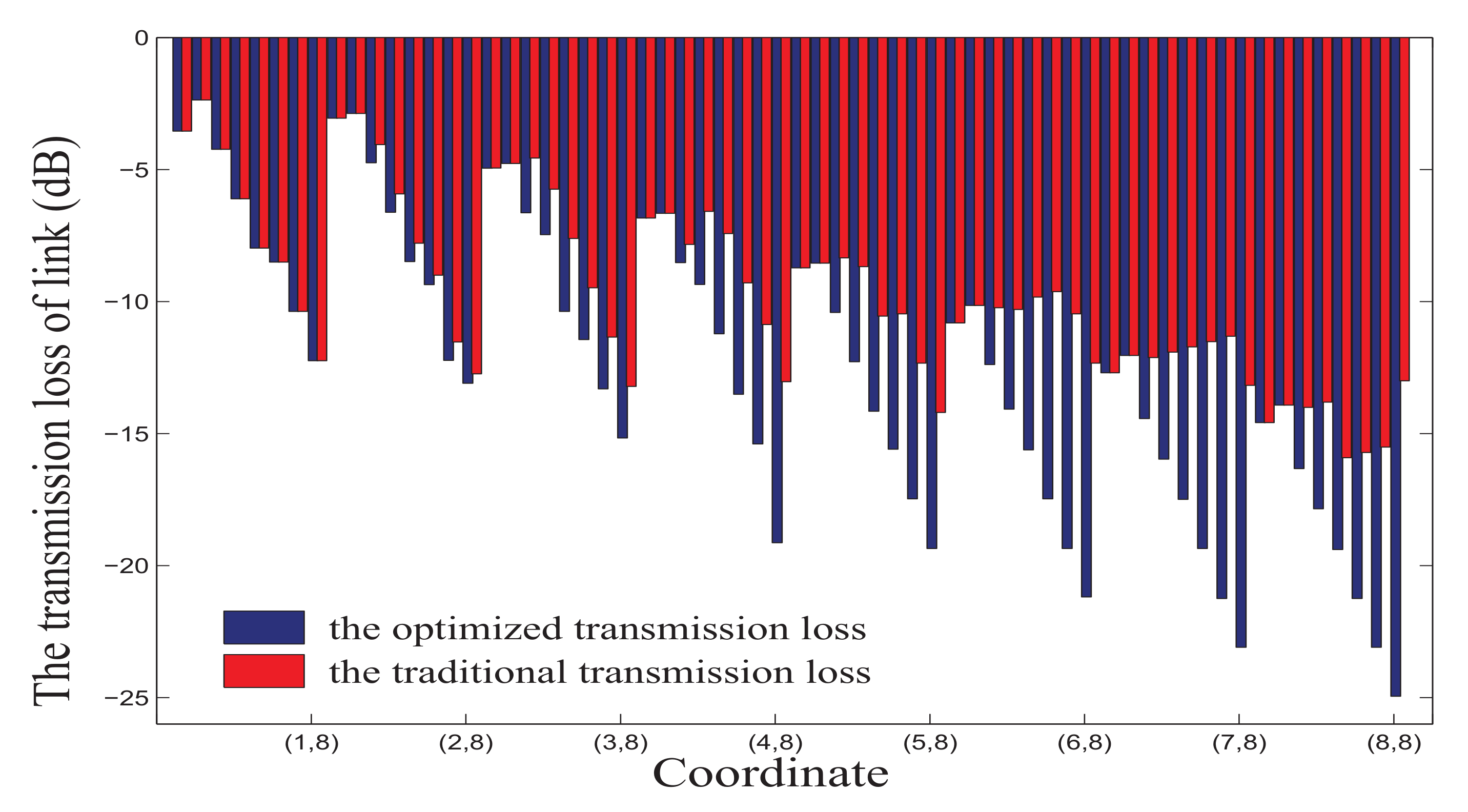
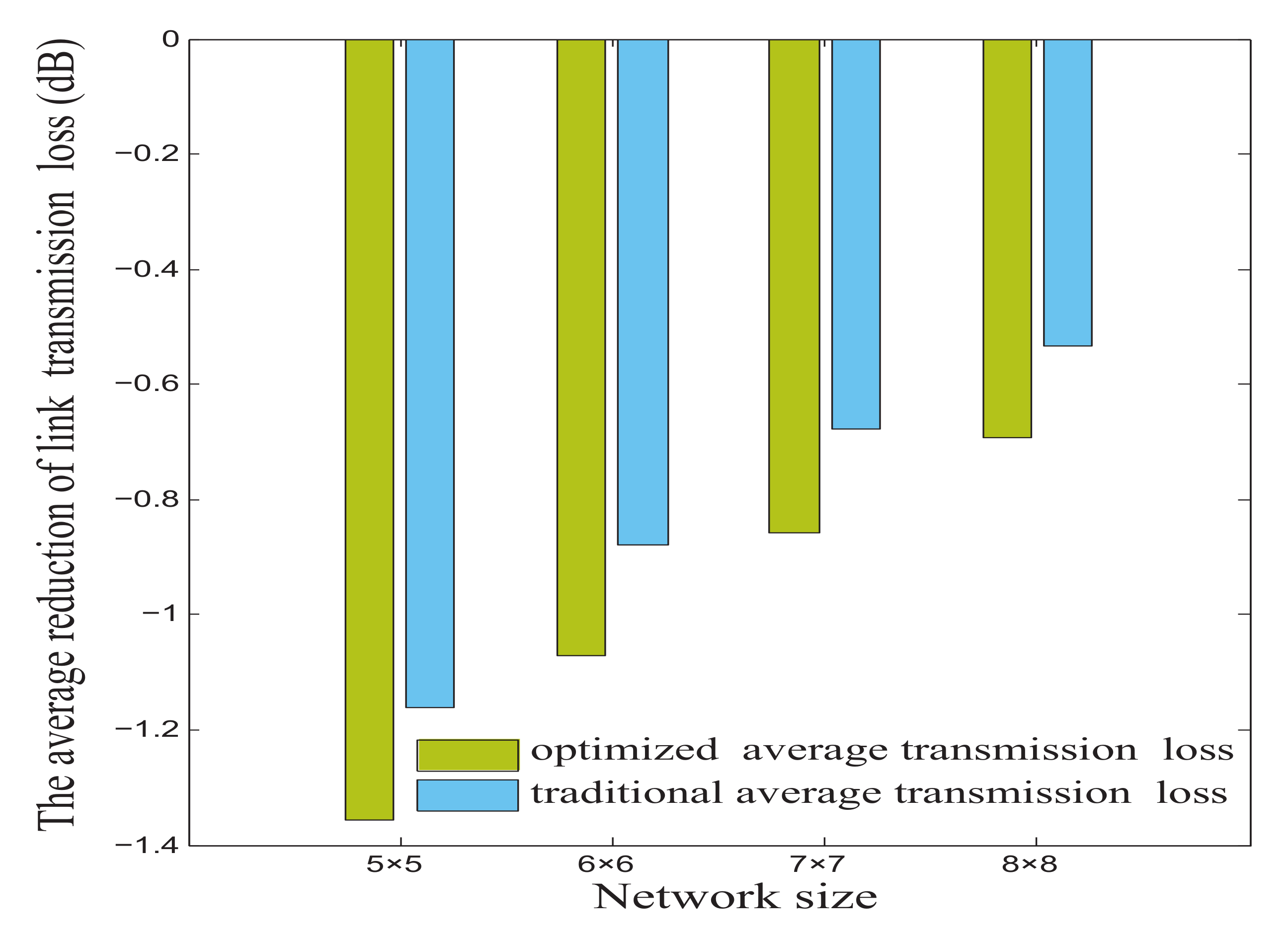
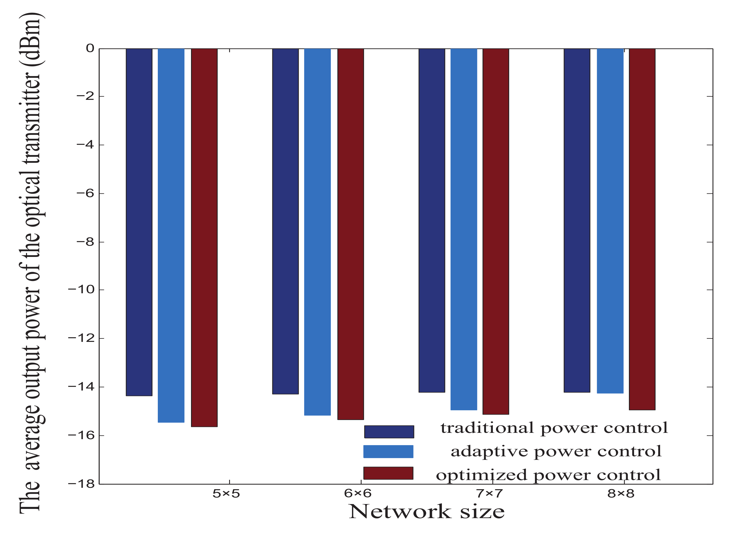
4.1. Transmission Loss and Average Output Power of Transmitter
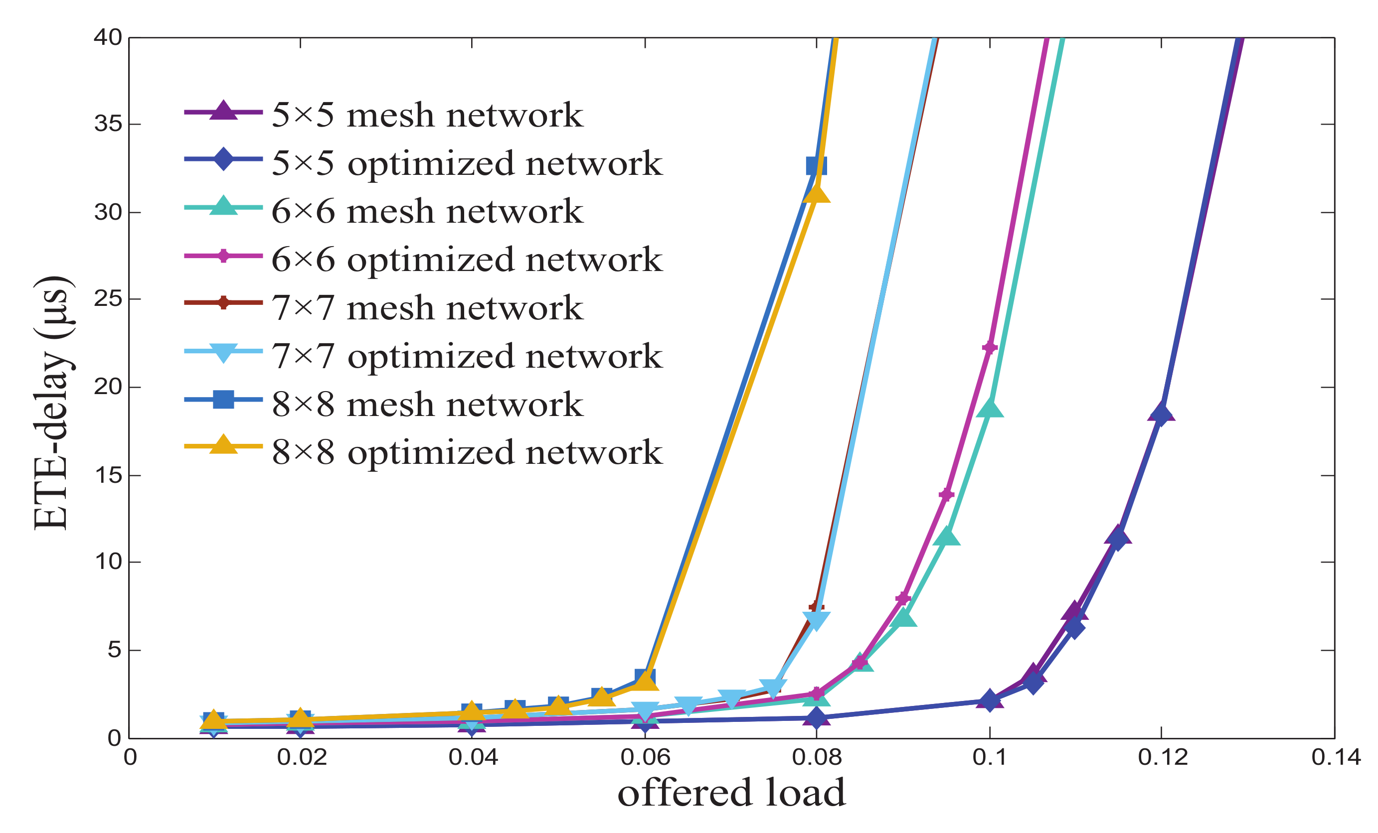
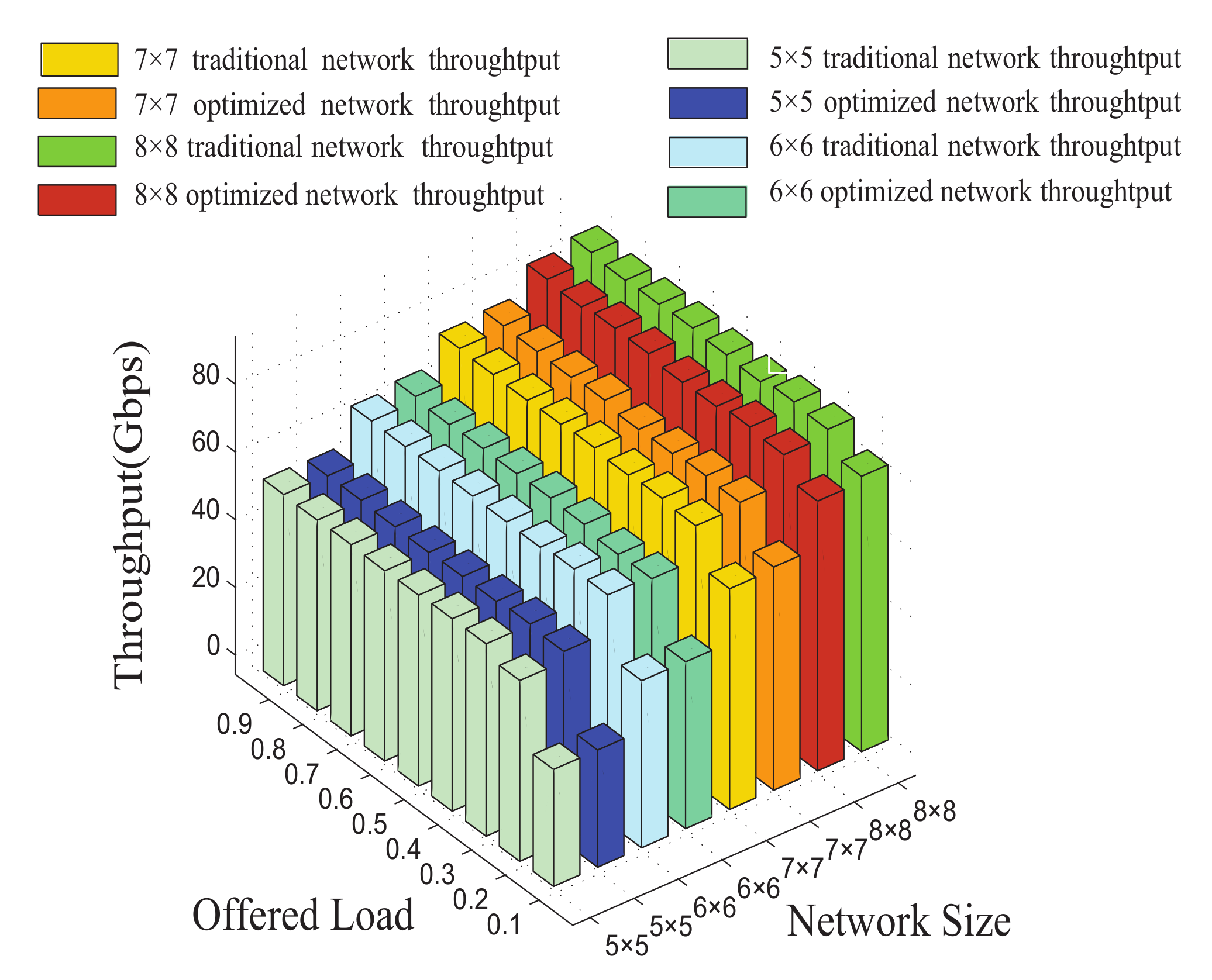
4.2. Network Performance Evaluation
5. Conclusions
Author Contributions
Funding
Conflicts of Interest
References
- Su, Y.; Xie, Y.Y.; Fu, L.X.; Chai, J.X. A Novel Architecture with Low Laser Power Based on Optical Networks-on-Chip. In Proceedings of the 2019 IEEE International Conference on Manipulation, Manufacturing and Measurement on the Nanoscale (3M-NANO), Zhenjiang, China, 4–8 August 2019. [Google Scholar]
- Ye, Y.Y.; Zhang, Z. A thermal-sensitive design of a 3D torus-based optical NoC architecture. Integration 2019, 68, 22–29. [Google Scholar] [CrossRef]
- Li, W.Z.; Hou, W.; Guo, B.L.; Li, X.; Zhou, Y.; Huang, S.G.; Rouskas, G.N. A large-scale nesting ring multi-chip architecture for manycore processor systems. Opt. Switch. Netw. 2019, 31, 183–192. [Google Scholar] [CrossRef]
- Yang, W.; Chen, Y.W.; Huang, Z.Y.; Zhang, H.B. RWADMM: Routing and Wavelength Assignment for Distribution-Based Multiple Multicasts in ONoC. In Proceedings of the IEEE International Conference ISPA/IUCC, Guangzhou, China, 12–15 December 2017; pp. 550–557. [Google Scholar]
- Fusella, E.; Cilardo, A. H2ONoC: A Hybrid Optical–Electronic NoC Based on Hybrid Topology. IEEE Trans. Very Large Scale Integr. Syst. 2017, 25, 330–343. [Google Scholar] [CrossRef]
- Wang, Z.H.; Xu, J.; Wu, X.W.; Ye, Y.Y.; Zhang, W.; Nikdast, M.; Wang, X.; Wang, Z. Floorplan Optimization of Fat-Tree-Based Networks-on-Chip for Chip Multiprocessors. IEEE Trans. Comput. 2012, 63, 1446–1459. [Google Scholar] [CrossRef]
- Gu, H.X.; Gu, H.X.; Yang, Y.T.; Wang, K.; Hao, Q.F. RPNoC: A Ring-Based Packet-Switched Optical Network-on-Chip. IEEE Photonics Technol. Lett. 2015, 27, 423–426. [Google Scholar]
- Song, T.T.; Xie, Y.Y.; Ye, Y.C.; Du, Y.C. Gaussian-based optical networks-on-chip: Performance analysis and optimization. Nano Commun. Netw. 2020, 24, 1–6. [Google Scholar] [CrossRef]
- Yang, X.P.; Song, T.T.; Ye, Y.C.; Liu, B.C.; Yan, H.; Zhu, Y.C.; Zheng, Y.L.; Liu, Y.; Xie, Y.Y. A Novel Algorithm for Routing Paths Selection in Mesh-Based Optical Networks-on-Chips. Micromachines 2020, 11, 996. [Google Scholar] [CrossRef]
- Xie, Y.Y.; Mahdi, N.; Xu, J.; Wu, X.W.; Zhang, W.; Ye, Y.Y.; Wang, X.; Wang, Z.H.; Liu, W.C. Formal worst-case analysis of crosstalk noise in mesh-based optical networks-on-chip. IEEE Trans. Very Large Scale Integr. Syst. 2013, 21, 1823–1836. [Google Scholar] [CrossRef]
- Chen, C.; Abellán, J.L.; Joshi, A. Managing Laser Power in Silicon-Photonic NoC Through Cache and NoC Reconfiguration. IEEE Trans. Comput. Aided Des. Integr. Circuits Syst. 2015, 34, 972–985. [Google Scholar] [CrossRef]
- Kao, Y.H.; Chao, H.J. Design of a Bufferless Photonic Clos Network-on-Chip Architecture. IEEE Trans. Comput. 2014, 63, 764–776. [Google Scholar]
- Bahareh, A.; Midia, R.; Ahmad, K. Extending the Power-Efficiency and Performance of Photonic Interconnects for Heterogeneous Multicores with Machine Learning. Photon. Netw. Commun. 2017, 34, 52–62. [Google Scholar]
- Chen, C.; Joshi, A. Runtime Management of Laser Power in Silicon-Photonic Multibus NoC Architecture. IEEE J. Sel. Top. Quantum Electron. 2013, 19, 3700713. [Google Scholar] [CrossRef]
- Kim, J.H.; Kim, H.N.; Bae, J.; Hur, N. Performance Analysis of Wideband Time Division Multiplexing for Low Power Broadcasting Transmission. In Proceedings of the 2019 25th Asia-Pacific Conference on Communications (APCC), Ho Chi Minh City, Vietnam, 6–8 November 2019. [Google Scholar]
- Wang, Z.Y.; Gu, H.X.; Yang, Y.T.; Zhang, B.X. Power Allocation Method for TDM-Based Optical Network on Chip. IEEE Photonics Technol. Lett. 2013, 25, 973–976. [Google Scholar] [CrossRef]
- Wu, X.W.; Xu, J.; Ye, Y.Y.; Wang, X.; Nikdast, M.; Wang, Z.H.; Wang, Z. An Inter/Intra-Chip Optical Network for Manycore Processors. IEEE Trans. Very Large Scale Integr. Syst. 2015, 23, 678–691. [Google Scholar]
- Thakkar, I.G.; Chittamuru, S.V.R.; Pasricha, S. Run-time laser power management in photonic NoCs with on-chip semiconductor optical amplifiers. In Proceedings of the 2016 Tenth IEEE/ACM International Symposium on Networks-on-Chip (NOCS), Nara, Japan, 31 August–2 September 2016; pp. 1–4. [Google Scholar]
- Zareei, M.; Vargas-Rosales, C.; Villalpando-Hernandez, R.; Azpilicueta, L.; Anisi, M.H.; Rehmani, M.H. The effects of an Adaptive and Distributed Transmission Power Control on the performance of energy harvesting sensor networks. Comput. Netw. 2018, 137, 69–82. [Google Scholar] [CrossRef]
- Duong, L.H.; Yang, P.; Wang, Z.; Chang, Y.S.; Xu, J.; Wang, Z.; Chen, X. Crosstalk Noise Reduction through Adaptive Power Control in Inter/Intra-Chip Optical Networks. IEEE Trans. Very Large Scale Integr. Syst. 2018, 38, 43–56. [Google Scholar] [CrossRef]
- Zhu, K.X.; Gu, H.X.; Yang, Y.T.; Tan, W.; Zhang, B.W. A 3D multilayer optical network on chip based on mesh topology. Photonic Netw. Commun. 2016, 32, 293–299. [Google Scholar] [CrossRef]
- Ding, W.Q.; Tang, D.H.; Liu, Y.; Chen, L.X.; Sun, X.D. Compact and low crosstalk waveguide crossing using impedance matched metamaterial. Appl. Phys. Lett. 2010, 96, 111114–111116. [Google Scholar] [CrossRef]
- Chan, J.; Hendry, G.; Bergman, K.; Carloni, L.P. Physical-layer modeling and system-level design of chip-scale photonic interconnection networks. IEEE Trans. Comput. Aided Des. Integr. Circuits Syst. 2011, 30, 1507–1520. [Google Scholar] [CrossRef]
- Ji, R.Q.; Yang, L.; Zhang, L.; Tian, Y.H.; Ding, J.F.; Chen, H.T.; Lu, Y.Y.; Zhou, P.; Zhu, W.W. Five-port optical router for photonic networks-on-chip. Opt. Express. 2011, 19, 20258–20268. [Google Scholar] [CrossRef]
- Nikdast, M.; Xu, J.; Wu, X.W.; Zhang, W.; Ye, Y.Y.; Wang, X.; Wang, Z.H.; Wang, Z. Systematic analysis of crosstalk noise in folded-torus-based optical networks-on-chip. IEEE Trans. Comput. Aided Des. Integr. Circuits Syst. 2014, 33, 437–450. [Google Scholar] [CrossRef]
- Ye, Y.Y.; Xu, J.; Wu, X.W.; Zhang, W.; Wang, X.; Nikdast, M. System-Level Modeling and Analysis of Thermal Effects in Optical Networks-on-Chip. IEEE Trans. Very Large Scale Integr. Syst. 2013, 21, 292–305. [Google Scholar] [CrossRef]
- Masini, G.; Capellini, G.; Witzens, J.; Gunn, C. A 1550 nm, 10 Gbps monolithic optical receiver in 130 nm CMOS with integrated Ge waveguide photodetector. In Proceedings of the 2007 4th IEEE International Conference on Group IV Photonics, Tokyo, Japan, 19–21 September 2007; pp. 1–3. [Google Scholar]
- Li, Z.Q.; Qouneh, A.; Joshi, M.; Zhang, W.Y.; Fu, X.; Li, T. Aurora: A Cross-Layer solution for thermally resilient photonic network-on-chip. IEEE Trans. Very Large Scale Integr. Syst. 2014, 23, 170–183. [Google Scholar]
- Bergman, K. Photonic Chip-Scale Interconnection Networks for Performance-Energy Optimized Computing. In Proceedings of the 2010 Fourth ACM/IEEE International Symposium on Networks-on-Chip, Grenoble, France, 3–6 May 2010. [Google Scholar]
- Wu, X.W.; Ye, Y.Y.; Xu, J.; Zhang, W.; Liu, W.C.; Nikdast, M.; Wang, X. UNION: A Unified Inter/Intrachip Optical Network for Chip Multiprocessors. IEEE Trans. Very Large Scale Integr. Syst. 2014, 22, 1082–1095. [Google Scholar]


Publisher’s Note: MDPI stays neutral with regard to jurisdictional claims in published maps and institutional affiliations. |
© 2021 by the authors. Licensee MDPI, Basel, Switzerland. This article is an open access article distributed under the terms and conditions of the Creative Commons Attribution (CC BY) license (http://creativecommons.org/licenses/by/4.0/).
Share and Cite
Zheng, Y.-L.; Song, T.-T.; Chai, J.-X.; Yang, X.-P.; Yu, M.-M.; Zhu, Y.-C.; Liu, Y.; Xie, Y.-Y. Exploring a New Adaptive Routing Based on the Dijkstra Algorithm in Optical Networks-on-Chip. Micromachines 2021, 12, 54. https://doi.org/10.3390/mi12010054
Zheng Y-L, Song T-T, Chai J-X, Yang X-P, Yu M-M, Zhu Y-C, Liu Y, Xie Y-Y. Exploring a New Adaptive Routing Based on the Dijkstra Algorithm in Optical Networks-on-Chip. Micromachines. 2021; 12(1):54. https://doi.org/10.3390/mi12010054
Chicago/Turabian StyleZheng, Yan-Li, Ting-Ting Song, Jun-Xiong Chai, Xiao-Ping Yang, Meng-Meng Yu, Yun-Chao Zhu, Yong Liu, and Yi-Yuan Xie. 2021. "Exploring a New Adaptive Routing Based on the Dijkstra Algorithm in Optical Networks-on-Chip" Micromachines 12, no. 1: 54. https://doi.org/10.3390/mi12010054
APA StyleZheng, Y.-L., Song, T.-T., Chai, J.-X., Yang, X.-P., Yu, M.-M., Zhu, Y.-C., Liu, Y., & Xie, Y.-Y. (2021). Exploring a New Adaptive Routing Based on the Dijkstra Algorithm in Optical Networks-on-Chip. Micromachines, 12(1), 54. https://doi.org/10.3390/mi12010054