Abstract
The optimal structure and process for the feedback field-effect transistor (FBFET) to operate as a logic device are investigated by using a technology computer-aided design mixed-mode simulator. To minimize the memory window of the FBFET, the channel length (Lch), thickness of silicon body (Tsi), and doping concentration (Nch) of the channel region below the gate are adjusted. As a result, the memory window increases as Lch and Tsi increase, and the memory window is minimum when Nch is approximately 9 × 1019 cm−3. The electrical coupling between the top and bottom tiers of a monolithic 3-dimensional inverter (M3DINV) consisting of an n-type FBFET located at the top tier and a p-type FBFET located at the bottom tier is also investigated. In the M3DINV, we investigate variation of switching voltage with respect to voltage transfer characteristics (VTC), with different thickness values of interlayer dielectrics (TILD), Tsi, Lch, and Nch. The variation of propagation delay of the M3DINV with different TILD, Tsi, Lch, and Nch is also investigated. As a result, the electrical coupling between the stacked FBFETs by TILD can be neglected. The switching voltage gaps increase as Lch and Tsi increase and decrease, respectively. Furthermore, the slopes of VTC of M3DINV increase as Tsi and Nch increase. For transient response, tpHL decrease as Lch, Tsi, and Nch increase, but tpLH increase as Lch and Tsi increase and it is almost the same for Nch.
1. Introduction
According to Moore’s Law, the number of transistors in integrated circuit (IC) chips is increasing with the improvements in semiconductor performance [1,2]. To improve the performance of next generation semiconductors, the requirement of integrating more transistors in a smaller area using nanoscaling is increasing. However, semiconductor devices with in scaling below 10 nm have fabrication challenges [3,4]. To overcome these challenges, monolithic 3-dimensional ICs (M3DICs) are attracting attention. M3DICs are designed with a transistor, a logic gate, and system blocks, which are integrated vertically to equip the M3DIC in accomplishing higher integration than a 2D conventional circuit. In ICs, each block is connected using a vertical interconnect that can be shorter than a horizontal interconnect and can achieve a lower critical delay [5,6,7,8,9,10,11]. Each vertically stacked block has an electrical coupling between the upper and lower tiers. Research on the application of monolithic 3D integration (M3DI) is being actively conducted and electrical coupling in the design of M3DI is being studied [11,12,13,14,15,16]. In particular, electrical coupling must be considered for the circuit design to achieve the desired performance.
Among the various applications of M3DI [17,18,19,20,21], the feedback field-effect transistor (FBFET) is in the spotlight as a next-generation device [22,23]. The FBFET has a S-shape energy band caused by p-n-p-n structure for n-type devices and it works on the principle of positive feedback. The positive feedback is caused by different types of doping in the channel region. Further to this, the channel region of FBFET is divided into two regions. One is the channel region below the gate and the other is channel region except for that below the gate. These two regions form an energy barrier owing to the n–p junction, and those regions form an energy barrier between the source/drain-side channel region and source/drain region, owing to the p–n junction. To operate the FBFET, the energy barrier caused by doping concentration of the source region and drain region must be removed. This process makes the energy band of the source-drain region parallel and achieves a clear saturation mode at on-state. When gate bias applied, the energy band is lower, and the electrons at the source region can flow along the drain-source electric field. Subsequently, electron stacks in the energy well formed between the channel and drain regions, and continuous stacking removed the energy well. This mechanism makes the energy band of all regions parallel and this happens in a short time [23]. According to the mechanism, FBFET has approximately zero subthreshold swing and hysteresis characteristics. Therefore, it can be used as a logic and memory device with the same structure. Various applications of FBFET were studied, such as using it as a logic device, a memory device, and a neuron circuit [24,25,26,27,28,29,30]. In the previous study, we investigated electrical coupling between vertically stacked FBFETs in the monolithic 3-dimensional inverter (M3DINV) with FBFETs, in terms of device characteristics [31]. However, studies on electrical interaction in terms of the electrical characteristics of an inverter are yet to be reported. The FBFET has a memory window, so it is necessary to investigate the changes in the electrical characteristics of the inverter. In addition, when configured with an M3DIC, an investigation of inverter characteristic variation is required for electrical coupling.
In this study, the electrical characteristics of an M3DINV consisting of vertically stacked FBFETs (M3DINV-FBFET) using a technology computer-aided design (TCAD) mixed-mode simulator are analyzed. The simulation structure parameters of M3DINV-FBFET are described in Section 2. In Section 3, the mechanism of FBFET through the energy bands is described. Moreover, the structure which memory windows of top N-type and bottom P-type FBFETs minimize is investigated with variation of its channel lengths, thickness of silicon body, and doping concentrations of the channel region. In addition, the extent to which the switching voltages of the voltage transfer characteristics (VTCs) and propagation delay of M3DINV-FBFET depend on the thickness of interlayer dielectrics (ILD) is described. Section 4 presents the conclusion of this study.
2. Simulation Structure Parameters
Figure 1a shows the 3D schematics of the M3DINV-FBFET and Figure 1b shows a-a’ cross-sectional views of the M3DINV-FBFET. The structure parameters are summarized in Table 1. Atlas [32] of Silvaco was used for the TCAD simulation. The 2D structure was used for simulation, as shown in Figure 1b. To simulate FBFET accurately, the models of bipolar junction transistor (BJT) and metal–oxide–semiconductor field-effect transistor (MOSFET), including the Lombardi concentration, voltage, and temperature (CVT) model, Shockley–Read–Hall model, Fermi–Dirac for MOSFET and field-dependent mobility model, Auger recombination model, and band gap narrowing model for BJT, are used. The simulation temperature was 300 K.
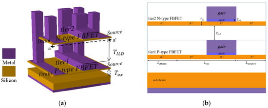
Figure 1.
(a) 3D schematic of M3DINV-FBFET; (b) a-a′ cross-sectional view of M3DINV-FBFET.

Table 1.
Structural parameters of M3DINV-FBFET used in technology computer-aided design (TCAD) simulation.
As shown in Figure 1b, the p-type and n-type FBFETs are located at Tier1 and Tier2, respectively. Gate-oxide was composed of hafnium dioxide (HfO2). The length of the gate was half the length of Lch and was located on the source-side in the channel region. The FBFET had a p-n-p-n/n-p-n-p (n-type/p-type) structure. Uniform doping concentrations in the n-type and p-type FBFETs were adopted in each region. The gate work functions of the p-type and n-type FBFETs were 4.8 and 4.6 eV, respectively.
3. Simulation Results
Figure 2 shows the energy band diagrams of n-type FBFET. The red and black lines denote conduction and valence bands, respectively. The symbols ‘e’ and’ ‘h’ represent electron and hole, respectively. To operate as FBFET, first, the energy barrier owing to the p–n junction between the drain–source region must be removed. As the drain–source voltage (Vds) applies to FBFET, the energy band of the drain and source regions is aligned, as shown in Figure 2a. When forward sweep is proceeded to FBFET, the energy band below the gate is lower. The electrons at the source region flow along the electric field and trap well in the energy, as shown in Figure 2b. The continuous stacking electrons remove the energy well. As a result, the energy band of all regions is aligned, as shown in Figure 2c. Moreover, all carriers flow freely along the electric field. By contrary, when reverse sweep is proceeded to FBFET at on-state, the energy band below the gate is higher and the energy barrier blocks the flow of carriers. As shown in Figure 2d, the energy barrier and well form owing to accumulating carriers.
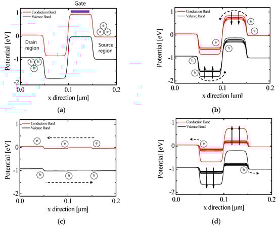
Figure 2.
Energy band diagram of n-type FBFET at Vds = 1 V. (a) Vgs = 0 V; (b) forward sweep, Vgs = 0 to 1 V; (c) Vgs = 1 V; and (d) reverse sweep, Vgs = 1 to 0 V.
Figure 3 shows the drain current–gate voltage (Ids − Vgs) characteristics and the drain current–drain voltage (Ids − Vds) characteristics of the top n-type and the bottom p-type FBFETs in the M3DINV-FBFET. An arrow pointing up denotes forward sweep, and pointing down denotes reverse sweep. FBFET works on a positive feedback when the carriers flow [22]. This mechanism causes a steep increase in current, as shown in Figure 3a. The difference in the threshold voltage between the forward and reverse sweeps is called the memory window. The memory window of p-type FBFET was 0.09 V at Vds = −1 V, and that of the n-type FBFET was 0.21 V at Vds = 1 V and Vpgs = 0 V, respectively.
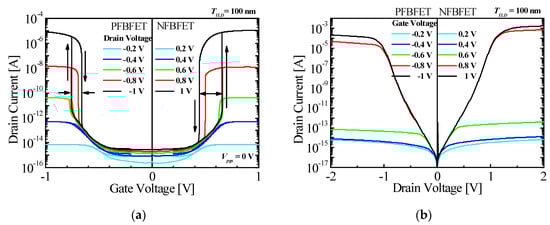
Figure 3.
Transfer characteristics of P-type and N-type FBFETs. (a) Ids−Vgs characteristics and (b) Ids−Vds characteristics.
3.1. Memory Window
For adjusting the memory window of the M3DINV-FBFET, various structure parameters of FBFET can be changed. In this study, the memory windows of the top and bottom FBFETs in the M3DINV-FBFET were investigated with the structure parameters Tsi, Lch, and Nch. Figure 4a shows the variation of memory window at different channel lengths. Channel length was changed from 80 to 160 nm. The memory windows of both types of FBFETs became smaller as Lch, was increased, as shown in Figure 4a. Memory window of the n-type FBFET was decreased from 0.21 V at 80 nm to 0.11 V at 160 nm and of the p-type, FBFET was decreased minutely from 0.09 V at 80 nm to 0.08 V at 160 nm. In addition, as Lch was increased, the threshold voltages of both types of FBFET were shifted in an arrow-direction, as shown in Figure 4a. To operate a device as logical, it must be minimized to approximately zero. However, the FBFET has a hysteresis with the memory window. To minimize the memory window, Lch for n-type was increased and that of p-type FBFETs was ~80 nm. Figure 4b shows the variation of memory window of the M3DINV-FBFET with TILD = 100 nm and Lch = 80 nm at different Tsi (from 4 to 30 nm). The memory window of both types of FBFETs became smaller as Tsi was increased, and the on-current of n-type FBFET was increased about ten times, as shown in Figure 4b. The memory window of n-type FBFET was decreased from 0.23 V at 4 nm to 0.14 V at 30 nm and that of p-type FBFET minutely was decreased from 0.09 V at 4 nm to 0.08 V at 30 nm. The threshold voltage of n-type FBFET was shifted in an arrow-direction, especially reverse sweep; however, the threshold voltage of p-type FBFET slight was shifted, as shown in Figure 4b. To minimize the memory window, Tsi was increased for both type of FBFETs.
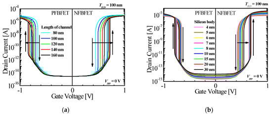
Figure 4.
Ids − Vgs characteristics of P-type and N-type FBFETs in M3DINV with different values of (a) Lch and (b) Tsi (TILD = 100 nm, for N-type FBFET, Vpgs = 0 V).
Figure 5 shows the variation of memory window according to Nch. The Nch was changed from 4 × 10¹⁹ to 4 × 1020 cm−3, and the structure parameter in Table 1, except for Nch, was used for the simulation. The black and red lines denote the memory windows of n-type and p-type FBFETs, respectively. The minimum memory window for n-type FBFET was 0.20 V at 9 × 1019 cm−3. The memory window for p-type FBFET was 0.05 V at 4 × 1019 cm−3, and that was increased to 0.32 V at 4 × 1020 cm−3, as the Nch was increased. To utilize FBFET for a logic device, the minimization of memory window is required, and thus, in this study, 1 × 1020 cm−3 was used for both types of FBFETs at the channel region below the gate.
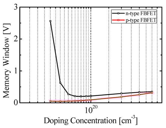
Figure 5.
The memory window with different value of Nch.
3.2. Voltage Transfer Characteristics
The VTC of the M3DINV-FBFET had a switching voltage gap between the forward and reverse sweeps. This occurs owing to the hysteresis characteristics of FBFET. In addition, the currents of M3DINV-FBFETs did not reach the clear on/off states. When the input voltage applied was 0 and 1 V, the output voltages were approximately 0.85 and 0.15 V, respectively. Switching voltage is affected by the electrical coupling between the top and bottom FBFETs and the window memory of FBFETs. Figure 6 shows VTC with different values of TILD. The inset in Figure 6 shows the magnification near switching voltage of the output. As the switching voltage gaps at TILD = 10 and 100 nm were approximately 12 and 10 mV, respectively, the change in the switching voltage gap because of TILD was miniscule. In this structure of the M3DINV-FBFET, the electrical coupling between the stacked FBFETs with respect to TILD can be neglected.
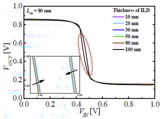
Figure 6.
Voltage transfer characteristics (VTC) of M3DINV-FBFET with Lch = 80 nm at different values of TILD.
Figure 7 shows the VTC with different values of Lch, Tsi, and Nch. As explained in Section 3.1, the memory window was decreased as Lch was increased; however, the switching voltage gap in the M3DINV-FBFET was increased, as shown in Figure 7a. The inset in Figure 7a shows the magnification near switching voltage of the output. The switching voltage gaps at Lch = 80 and 160 nm were approximately 10 and 50 mV, respectively. The variation of VTC of the M3DINV-FBFET with different Tsi is shown in Figure 7b. The memory window was decreased as Tsi was increased, as explained in Section 3.1; however, the switching voltage gap and slope of the M3DINV-FBFET was increased and decreased a little, respectively, as shown in Figure 7b. The variation of VTC of the M3DINV-FBFET with different values of Nch is shown in Figure 7c. In the simulation, the values of Nch of top n-type and bottom p-type FBFETs are the same with different types. The slope of the M3DINV-FBFET was increased as the Nch was increased, and the VTC for the inverter disappeared at the doping concentration of below 4 × 1019 cm−3. For better VTC of the M3DINV-FBFET, the doping concentration of over 9 × 1019 cm−3 is required. As shown in Figure 7, the switching voltage gap significantly is affected by Lch and Nch, because the threshold voltage of forward and reverse sweep is changed according to variation of Lch and Nch. Meanwhile, the switching voltage gaps with different values of Tsi is almost the same, because the threshold voltage is changed minutely at forward sweep and reverse sweep.
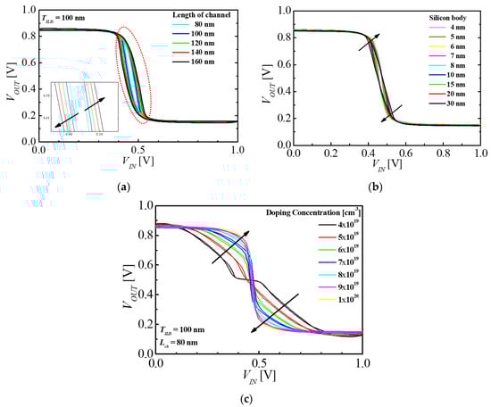
Figure 7.
VTC of M3DINV-FBFET with TILD = 100 nm at different values of (a) Lch, (b) Tsi, and (c) Nch.
3.3. Transient Response
Figure 8 shows the transient simulation results of the M3DINV-FBFET at time steps of 1 μs, 1 ms, and 1 s. For simulating the transient response of the M3DINV-FBFET, a time step of at least 1 ms is required for desirable inverter characteristics. The structure parameter of the M3DINV-FBFET in Table 1 was used for simulation.
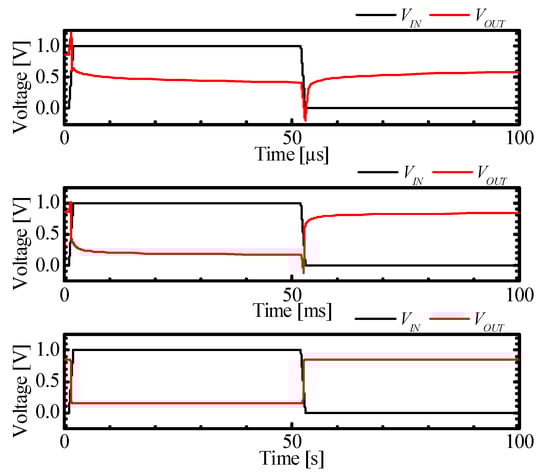
Figure 8.
Transient response with 1 μs, 1 ms, and 1 s time steps.
Figure 9 shows the transient response results of the M3DINV-FBFET with different values of TILD, Lch, Tsi, and Nch. The insets in Figure 9 show the magnification near ‘0.5 V’ of output. The black line denotes clock and the other lines are output. The time step used is 1 s, which shows the desirable inverter characteristics among the results shown in Figure 8. High to low delay (tpHL) and low to high delay (tpLH) of the M3DINV-FBFET with the parameters in Table 1 are 28 and 46 ms, respectively. As TILD was decreased from 100 to 10 nm, tpHL was increased from 28 to 29 ms, and tpLH was almost the same, as shown in Figure 9a. As Lch was increased from 80 to 160 nm, tpHL was decreased from 29 to 6 ms; however, tpLH was increased from 46 to 70 ms, as shown in Figure 9b. As Tsi was increased from 4 to 30 nm, tpHL decreased from 29 to 24 ms, whereas tpLH was increased 44 to 49 ms, as shown in Figure 9c. As Nch increases from 4 × 10¹⁹ to 1 × 1020 cm−3, tpHL decreased from 53 to 28 ms, whereas tpLH was almost the same, as shown in Figure 9d. The variation of tpHL and tpLH by TILD was very small and thus, the electrical coupling between the stacked FBFETs with respect to TILD can be neglected. As all Lch, Tsi, and Nch increased, all the tpHL decreased, whereas the tpLH increased, increased, and was almost the same, respectively.
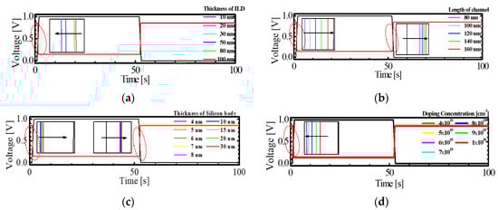
Figure 9.
Transient response simulation results with different values of (a) TILD, (b) Lch, (c) Tsi, and (d) doping concentration of channel region below the gate.
4. Conclusions
In this study, we investigated the optimum structure of top n-type and bottom p-type FBFETs in an M3DINV-FBFET to minimize the memory window of each FBFET using TCAD mixed-mode simulation. Furthermore, the electrical coupling between the top and bottom tiers in the M3DINV-FBFET was studied. First, we investigated the memory window with the various values of Lch, Tsi, and Nch of FBFETs in the M3DINV-FBFET. It was observed that as all the Lch and Tsi increase, all the memory windows decreased. The minimum memory window for n-type FBFET is 0.20 V at 9 × 1019 cm−3, and that of p-type FBFET was increased as Nch increased. In the M3DINV-FBFET, the VTC had a switching voltage gap owing to the hysteresis characteristics of FBFET. The variation of switching voltage gap by TILD was very small (~10 mV), and thus, the electrical coupling between the stacked FBFETs with respect to TILD can be neglected. The switching voltage gap increased as Lch and Tsi increased and decreased, respectively. Furthermore, the slope of VTC of the M3DINV-FBFET increased, as the Tsi and Nch increased. The transient response of the M3DINV-FBFET was investigated with respect to TILD, Lch, Tsi, and Nch. The variation of tpHL and tpLH by TILD was very small and thus, the electrical coupling between the stacked FBFETs with respect to TILD can be neglected. As all Lch, Tsi, and Nch increased, all the tpHL decreased, whereas the tpLH increased, increased, and was almost the same, respectively. Even though conclusively, the M3DINV-FBFET may be tedious to use in logic circuits due to ambiguous on/off states and the relatively slow time response (approximately several decade ms), it is necessary to further investigate the optimal structure and process for the FBFET to operate as a logic device.
Author Contributions
Conceptualization, J.H.O. and Y.S.Y.; methodology, J.H.O. and Y.S.Y.; investigation, J.H.O. and Y.S.Y.; data curation, J.H.O.; writing—original draft preparation, J.H.O.; writing—review and editing, J.H.O. and Y.S.Y.; supervision, Y.S.Y.; project administration, Y.S.Y.; funding acquisition, Y.S.Y. All authors have read and agreed to the published version of the manuscript.
Funding
This research was supported by the Basic Science Research Program through NRF of Korea funded by the Ministry of Education (NRF-2019R1A2C1085295).
Acknowledgments
This work was supported by IDEC (EDA tool).
Conflicts of Interest
The authors declare no conflict of interest.
References
- Waldrop, M.M. The chips are down for Moore’s law. Nature 2016, 530, 144–147. [Google Scholar] [CrossRef] [PubMed]
- Kuhn, K.J.; Giles, M.D.; Becher, D.; Kolar, P.; Kornfeld, A.; Kotlyar, R.; Ma, S.T.; Maheshwari, A.; Mudanai, S. Process Technology Variation. IEEE Trans. Electron Devices 2011, 58, 2197–2208. [Google Scholar] [CrossRef]
- Chen, T. Overcoming research challenges for CMOS scaling: Industry directions. In Proceedings of the 2006 8th International Conference on Solid-State and Integrated Circuit Technology Proceedings, Shanghai, China, 23–26 October 2006; pp. 4–7. [Google Scholar] [CrossRef]
- Claverlier, L.; Deguet, C.; Di Cioccio, L.; Augendre, E.; Brugere, A.; Gueguen, P.; Le Tiec, Y.; Moriceau, H.; Rabarot, M.; Signamarcheix, T.; et al. Engineered substrates for future More Moore and More than Moore integrated devices. In Proceedings of the 2010 IEEE International Electron Devices Meeting (IEDM), San Francisco, CA, USA, 6–8 December 2010; pp. 2.6.1–2.6.4. [Google Scholar] [CrossRef]
- Black, B.; Annavaram, M.; Brekelbaum, N.; Devale, J.; Jiang, L.; Loh, G.H.; McCaule, D.; Morrow, P.; Nelson, W.; Pantuso, D.; et al. Die Stacking (3D) Microarchitecture. In Proceedings of the 2006 39th Annual IEEE/ACM International Symposium on Microarchitecture (MICRO’06), Orlando, FL, USA, 9–13 December 2006; pp. 469–479. [Google Scholar] [CrossRef]
- Davis, W.R.; Wilson, J.; Mick, S.; Xu, J.; Hua, H.; Mineo, C.; Sule, A.M.; Steer, M.; Franzon, P.D. Demystifying 3D ICs: The pros and cons of going vertical. IEEE Des. Test Comp. 2005, 22, 498–510. [Google Scholar] [CrossRef]
- Knickerbocker, J.U.; Andry, P.S.; Dang, B.; Horton, R.R.; Interrante, M.J.; Patel, C.S.; Polastre, R.J.; Sakuma, K.; Sirdeshmukh, R.; Sprogis, E.J.; et al. Three-dimensional silicon integration. IBM J. Res. Dev. 2008, 52, 553–569. [Google Scholar] [CrossRef]
- Vinet, M.; Batude, P.; Tabone, C.; Previtali, B.; LeRoyer, C.; Pouydebasque, A.; Clavelier, L.; Valentian, A.; Thomas, O.; Michaud, S.; et al. 3D monolithic integration: Technological challenges and electrical results. MicroElectron Eng. 2011, 88, 331–335. [Google Scholar] [CrossRef]
- Cheramy, S.; Jouve, A.; Arnaud, L.; Fenouillet-Beranger, C.; Batude, P.; Vinet, M. Towards high density 3D interconnections. In Proceedings of the 2016 IEEE International 3D Systems Integration Conference (3DIC), San Francisco, CA, USA, 8–11 November 2016; pp. 1–5. [Google Scholar] [CrossRef]
- Wong, S.; El-Gamal, A.; Griffin, P.; Nishi, Y.; Pease, F.; Plummer, J. Monolithic 3D integrated circuits. In Proceedings of the 2007 International Symposium on VLSI Technology, Systems and Applications (VLSI-TSA), Hsinchu, Taiwan, 23–25 April 2007; pp. 1–4. [Google Scholar] [CrossRef]
- Panth, S.; Samal, S.; Yu, Y.S.; Lim, S.K. Design challenges and solutions for ultra-high-density monolithic 3D ICs. In Proceedings of the 2014 SOI-3D-Subthreshold Microelectronics Technology Unified Conference (S3S), Millbrae, CA, USA, 6–9 October 2014; pp. 1–2. [Google Scholar] [CrossRef]
- Yu, Y.S.; Panth, S.; Lim, S.K. Electrical coupling of monolithic 3-D inverters. IEEE Trans. Electron Devices 2016, 63, 3346–3349. [Google Scholar] [CrossRef]
- Koneru, A.; Chakrabarty, K. Analysis of electrostatic coupling in monolithic 3D integrated circuits and its impact on delay testing. In Proceedings of the 2016 21st IEEE European Test Symposium (ETS), Amsterdam, The Netherlands, 25 July 2016; pp. 1–6. [Google Scholar] [CrossRef]
- Fan, M.; Hu, V.P.; Chen, Y.; Su, P.; Chuang, C. Investigation and optimization of monolithic 3D logic circuits and SRAM cells considering interlayer coupling. In Proceedings of the 2014 IEEE International Symposium on Circuits and Systems (ISCAS), Melbourne, Australia, 1–5 June 2014; pp. 1130–1133. [Google Scholar] [CrossRef]
- Lim, S.K. Bringing 3D ICs to Aerospace: Needs for Design Tools and Methodologies. J. Inf. Commun. Converg. Eng. 2017, 15, 117–122. [Google Scholar] [CrossRef]
- Sideris, P.; Brunet, L.; Sicard, G.; Batude, P.; Theodorou, C. Impact of Inter-Tier Coupling on Static and Noise Performance in 3D Sequential Integration Technology. In Proceedings of the 2019 Joint International EUROSOI Workshop and International Conference on Ultimate Integration on Silicon (EUROSOI-ULIS), Grenoble, France, 1–3 April 2019; pp. 1–4. [Google Scholar] [CrossRef]
- Sekar, D.C.; Or-Bach, Z. Monolithic 3D-ICs with single crystal silicon layers. In Proceedings of the 2011 IEEE International 3D Systems Integration Conference (3DIC), 2011 IEEE International, Osaka, Japan, 31 January–2 February 2012; pp. 1–2. [Google Scholar] [CrossRef]
- Jiang, J.; Parto, K.; Cao, W.; Banerjee, K. Monolithic-3D Integration with 2D Materials: Toward Ultimate Vertically-Scaled 3D-ICs. In Proceedings of the 2018 IEEE SOI-3D-Subthreshold Microelectronics Technology Unified Conference (S3S), Burlingame, CA, USA, 15–18 October 2018; pp. 1–3. [Google Scholar] [CrossRef]
- Shulaker, M.M.; Wu, T.F.; Pal, A.; Zhao, L.; Nishi, Y.; Saraswat, K.; Wong, H.-S.P.; Mitra, S. Monolithic 3D integration of logic and memory: Carbon nanotube FETs, resistive RAM, and silicon FETs. In Proceedings of the 2014 IEEE International Electron Devices Meeting (IEDM), San Francisco, CA, USA, 4–6 December 2014; pp. 27.4.1–27.4.4. [Google Scholar] [CrossRef]
- Vollebregt, S.; Ishihara, R.; van der Cingel, J.; Beenakker, K. Low-temperature bottom-up integration of carbon nanotubes for vertical interconnects in monolithic 3D integrated circuits. In Proceedings of the 2011 IEEE International 3D Systems Integration Conference (3DIC), 2011 IEEE International, Osaka, Japan, 31 January–2 February 2012; pp. 1–4. [Google Scholar] [CrossRef]
- Golshani, N.; Derakhshandeh, J.; Ishihara, R.; Beenakker, C.I.M.; Robertson, M.; Morrison, T. Monolithic 3D integration of SRAM and image sensor using two layers of single grain silicon. In Proceedings of the 2010 IEEE International 3D Systems Integration Conference (3DIC), Munich, Germany, 16–18 November 2010; pp. 1–4. [Google Scholar] [CrossRef]
- Lee, C.; Ko, E.; Shin, C. Steep slope silicon-on-insulator feedback field-effect transistor: Design and performance analysis. IEEE Trans. Electron Devices 2019, 66, 286–291. [Google Scholar] [CrossRef]
- Lee, C.; Sung, J.; Shin, C. Understanding of Feedback Field-Effect Transistor and Its Applications. Appl. Sci. 2020, 10, 3070. [Google Scholar] [CrossRef]
- Kwon, M.; Hwang, S.; Baek, M.; Cho, S.; Park, B. Dual gate positive feedback field-effect transistor for low power analog circuit. In Proceedings of the 2017 Silicon Nanoelectronics Workshop (SNW), Kyoto, Japan, 4–5 June 2017; pp. 115–116. [Google Scholar] [CrossRef]
- Woo, S.; Cho, J.; Lim, D.; Cho, K.; Kim, S. Transposable 3T-SRAM Synaptic Array using Independent Double-Gate Feedback Field-Effect Transistors. IEEE Trans. Electron Devices 2019, 66, 4753–4758. [Google Scholar] [CrossRef]
- Yeung, C.W.; Padilla, A.; Liu, T.J.K.; Hu, C. Programming characteristics of the steep turn-on/off feedback FET (FBFET). In Proceedings of the 2009 Symposium on VLSI Technology, Honolulu, HI, USA, 16–18 June 2009; pp. 176–177. [Google Scholar]
- Kang, H.; Cho, J.; Kim, Y.; Lim, D.; Woo, S.; Cho, K.; Kim, S. Nonvolatile and volatile memory characteristics of a silicon nanowire feedback field-effect transistor with a nitride charge-storage layer. IEEE Trans. Electron Devices 2019, 66, 3342–3348. [Google Scholar] [CrossRef]
- Cho, J.; Lim, D.; Woo, S.; Cho, K.; Kim, S. Static random access memory characteristics of single-gated feedback field-effect transistors. IEEE Trans. Electron Devices 2019, 66, 413–419. [Google Scholar] [CrossRef]
- Woo, S.; Cho, J.; Lim, D.; Park, Y.; Cho, K.; Kim, S. Implementation and characterization of an integrate-and-fire neuron circuit using a silicon nanowire feedback field-effect transistor. IEEE Trans. Electron Devices 2020, 67, 2995–3000. [Google Scholar] [CrossRef]
- Kwon, M.; Park, K.; Baek, M.; Lee, J.; Park, B. A Low-Energy High-Density Capacitor-Less I&F Neuron Circuit Using Feedback FET Co-Integrated With CMOS. IEEE J. Electron Devices Soc. 2019, 7, 1080–1084. [Google Scholar] [CrossRef]
- Oh, J.H.; Yu, Y.S. Observation of electrical characteristics of monolithic 3D integrated circuits consisting of feedback field-effect transistor. In Proceedings of the 27th Korean Conference on Semiconductors (KCS), Gwangwon-do, Korea, 12–14 February 2020; p. 625. [Google Scholar]
- Silvaco Int. ATLAS ver. 5. 20. 2. R Manual; Silvaco Int.: Santa Clara, CA, USA, 2015. [Google Scholar]
© 2020 by the authors. Licensee MDPI, Basel, Switzerland. This article is an open access article distributed under the terms and conditions of the Creative Commons Attribution (CC BY) license (http://creativecommons.org/licenses/by/4.0/).