Review

Research Status and Development Trend of MEMS Switches: A Review

State Key Laboratory for Manufacturing System Engineering, Xi’an Jiaotong University, Xi’an 710049, China
*
Authors to whom correspondence should be addressed.
Micromachines 2020, 11(7), 694; https://doi.org/10.3390/mi11070694
Submission received: 18 June 2020 / Revised: 11 July 2020 / Accepted: 16 July 2020 / Published: 17 July 2020
(This article belongs to the Special Issue Micro-Manufacturing and Applications)

Abstract

:
MEMS switch is a movable device manufactured by means of semiconductor technology, possessing many incomparable advantages such as a small volume, low power consumption, high integration, etc. This paper reviews recent research of MEMS switches, pointing out the important performance indexes and systematically summarizing the classification according to driving principles. Then, a comparative study of current MEMS switches stressing their strengths and drawbacks is presented, based on performance requirements such as driven voltage, power consumption, and reliability. The efforts of teams to optimize MEMS switches are introduced and the applications of switches with different driving principles are also briefly reviewed. Furthermore, the development trend of MEMS switch and the research gaps are discussed. Finally, a summary and forecast about MEMS switches is given with the aim of providing a reference for future research in this domain.

1. Introduction

Switches are essentially used to control the on–off state of circuits and are required to react quickly and accurately to signals. The MEMS switch device is a tiny movable element with three-dimensional structure fabricated by semiconductor technology. MEMS switches offer much lower power consumption, much better isolation, and lower insertion loss compared to conventional field-effect transistors and p-i-n diode switches [1,2,3], and they possess advantages such as small size and high integration. The rise of MEMS switches provides strong technical support for the development of signal control systems. At present, the demand for MEMS switches mainly comes from military security systems [4,5,6,7], the automobile industry [8,9], the wireless communication field [10,11,12,13,14,15], medical apparatus and instruments [9,16], micro-optical electromechanical systems (MOEMS) [17,18,19] and more. Over the last few decades, various types of MEMS switches have been developed. To be familiar with the working mechanism and optimization direction of existing MEMS switches is of great significance for the development of innovative MEMS switches. However, there is a lack of a comprehensive classification of MEMS switches.
MEMS switches can be classified in a variety of ways [20], such as according to whether there is an additional driving source, and the existing MEMS switches can be segmented into passive MEMS switches and active MEMS switches. Passive MEMS switches exploit their own system to induce changes and absorb energy for inertial actuation [21,22]. This driving principle has better long-term storage performance and resistance to electromagnetic interference owing to no need for extra energy [23]. Active drive refers to the use of external energy to drive movable electrodes to change the on–off state of switches. The drive of MEMS switches involves magnetic energy, electrical energy, photochemical energy and other energy fields, which are converted into mechanical energy to generate displacement [24,25].
MEMS switches can be roughly divided into silicon-based MEMS switches and non-silicon-based MEMS switches according to the different processing materials. Silicon-based MEMS switches are usually fabricated on SOI (silicon-on-insulator) wafers with the advantages of high shape precision and a simple process [26,27]. However, if the structural layer material of the silicon-based switch is used directly for contacts, the contact resistance will be too large compared with conductor materials, resulting in an unobvious signal. To reduce the contact resistance, it is necessary to apply a layer of low-resistivity metal on the contact surface of the electrodes [28]. In addition, silicon is not suitable for high impact and high load applications either as a structure layer or as a substrate [29]. On the other hand, non-silicon switches are mainly fabricated from LIGA (lithographie, galvanoformung and abformung) or ultra-precision processing technology. For metal-based switches, multi-layer suspended movable structures are usually fabricated from Ni via micro-electroplating [30,31,32]. In contrast to the properties of silicon-based switches, metal structures provide excellent electrical conductivity, as well as good mechanical properties and toughness. Although this switch solves the problem of high contact resistance, the maturity of metal microstructures manufacturing is relatively low. During processing, the structure is prong to deformation [33], leading to a low yield.
What is more, according to the contact modes, MEMS switches can be grouped into resistive switches and capacitive switches, a classification quite common seen in RF (radio frequency) MEMS applications. Capacitive switches are turned on or off through capacitance coupling [34], and these types of switches are suitable for high-frequency (about 3 MHz to 30 MHz) applications [35,36]. On the other hand, resistive switches are generally used in the lower frequency band (about 30 KHz to 300 KHz) of the radio frequency signal [37]. Low contact resistance, usually less than 1–2 ohms, is one of the important performance requirements of MEMS switches [38].
Of course, MEMS switches can be divided into laterally actuated switches [13,39,40,41,42] and vertically actuated switches [43,44,45] The displacement of vertically actuated switches is out-of-plane while that of laterally actuated switches is in-plane.
This review aims to provide detailed insights into the structural design and performance optimization of MEMS switches, based on the literature of the last 20 years. In the second part, the key performance indexes of MEMES switches, especially the influencing factors of reliability, are pointed out. The third part, as the main body of the paper, introduces in detail the different principles of switches and the targeted performance optimization from the aspect of structure. Thereinto, bistable mechanism is used in almost every actuation as an effective method to enhance the contact effect and improve the switching speed. In the design of active switch, there is also the problem of how to realize the insulation between drive signal and switch signal, which has been also mentioned in each section. Each switch has its pros and cons, so designers have made specific improvements to the switches after trade-offs or analyzing the application requirements. Furthermore, the general development trend of MEMS switches is predicted. This review serves the purpose of providing researchers in this field with a reference source.

2. Performance Indicators of MEMS Switches

In the development of MEMS switches, their performance is constantly optimized. The key performance indicators of MEMS switches are driving voltage, switching time, power consumption, reliability and so on. Among them, the reliability of MEMS switches is a factor that must be considered in performance design. The neglect of reliability is a major obstacle to the ultimate commercialization of switches. In order to improve the reliability of switches, possible failure modes of switches should be analyzed first. Table 1 below is an analysis of common failure modes of MEMS switches.
To analyze the failure of MEMS switches in detail, capacitive switches and resistive switches should be considered separately. The main problem affecting the reliability of capacitive switches is not the mechanical properties, but the charging issue. The rate of the C/V curve [46] and the stretched exponential for charging [47] can be used to evaluate the failure time of capacitor switches. Goldsmith [48] proposed an efficient accelerated life test method, where a continuous electrical signal is applied to the switch and detects the modulation signal generated by the switch action. The reason for this failure is assumed to be the continuous accumulation of electric charge in the dielectric layer, which eventually leads to the driving voltage drift or latch-up effect. The optimization of capacitive switches should solve the problem of charge accumulation [49]. On the one hand, it can be improved by optimizing the dielectric material such as the dielectric layer material with high dielectric coefficient and low trap density [48,49,50,51,52]. A dielectric-less switch has proved to be an effective method [53]. On the other hand, the voltage can be optimized, such as using high voltage to drive the switch to close and low voltage to maintain the closed state [54], or using bipolar control voltage [55].
The failure of the resistive switches is due to contact fatigue. Mechanical stress causes deformation and wear of contact surfaces, while electrical stress mainly causes electromigration and melting of contact surfaces. Their combined action eventually leads to increased contact resistance or adhesion. Therefore, the choice of contact material is the key to the reliability of the switch, considering such factors as hardness, resistivity, melting point and sensitivity to organic pollutants [56,57]. Soft metals, such as gold, are suitable for reducing contact resistance, but their contact surfaces are prone to microwelding. Ke et al. [58] coated Au contacts with Ru to investigate placing harder materials on top of softer materials for a lifetime enhancement. Yang et al. [59] showed Au–Ni alloy contacts resist material transfer better than Au–Au contacts. In exchange, alloying Au with other metals also results in an increased resistivity. Yaglioglu et al. [60] examined the electrical contact properties of carbon nanotube (CNT)-coated surfaces. The high Young’s modulus and potential for low resistance of CNTs makes them suitable candidates for micro-switch contacts. Experiments have shown that adding a small amount of Pd or Pt to the gold increases the lifetime of the device, but the contact resistance increases only a small amount [38]. In order to prevent the degradation of switch contact, apart from preventing the mechanical damage of the contact surface, it is necessary to improve the sealing of the packaging to prevent organic or inorganic pollution [61].
Both residual stress and temperature affect the switching capabilities of MEMS switches. This means that changes in operating temperature or increases in residual stress may increase the actuation voltage of MEMS switches. The actual driving voltage of the switch is often very different from the design value. One of the reasons is the influence of residual stress. The residual stress in the movable structure will accelerate the fatigue and reduce the durability of MEMS switches [62]. Residual stress formed during micro-machining is the main factor that affects the reliability of MEMS switches [63,64]. Thermal residual stress is generated during the thermal loading-unload cycles during the plasma etching stage. In surface micromachining process, multilayer metals are deposited on the substrate. The difference between the thermal expansion coefficient of different material layers leads to the formation of residual stress. It affects the flatness of the fabricated switch, thus affecting the static and dynamic characteristics of the switch. For example, the compressive stress increases the pull-in voltage and reduces the switching time [65]. Temperature is the most common failure acceleration factor. The experimental results show that the change in temperature accelerates the failure modes, such as charge capture, mechanical creep and contact degradation [66].
The key performance of the switch, such as driving voltage and switching time, is closely related to the driving principles. Therefore, it is necessary to introduce the principles and optimization performance structurally of each driving mode, respectively and in detail.

3. Classification of MEMS Switches Based on Driving Principles

According to the driving principles [67], MEMS mechanical switches can be roughly divided into passive inertial switches, electrostatic switches, electro-thermal switches, electromagnetic switches, piezoelectric switches and shape memory alloy switches [68], etc. Table 2 provides a summary of the key performance comparison of several mainstream MEMS mechanical switches.

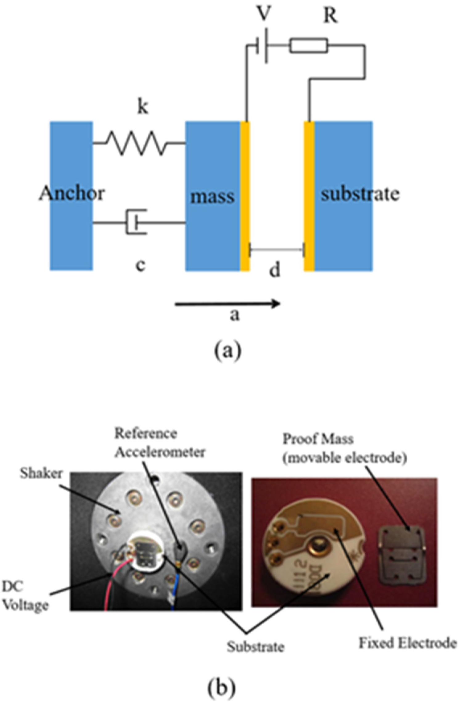
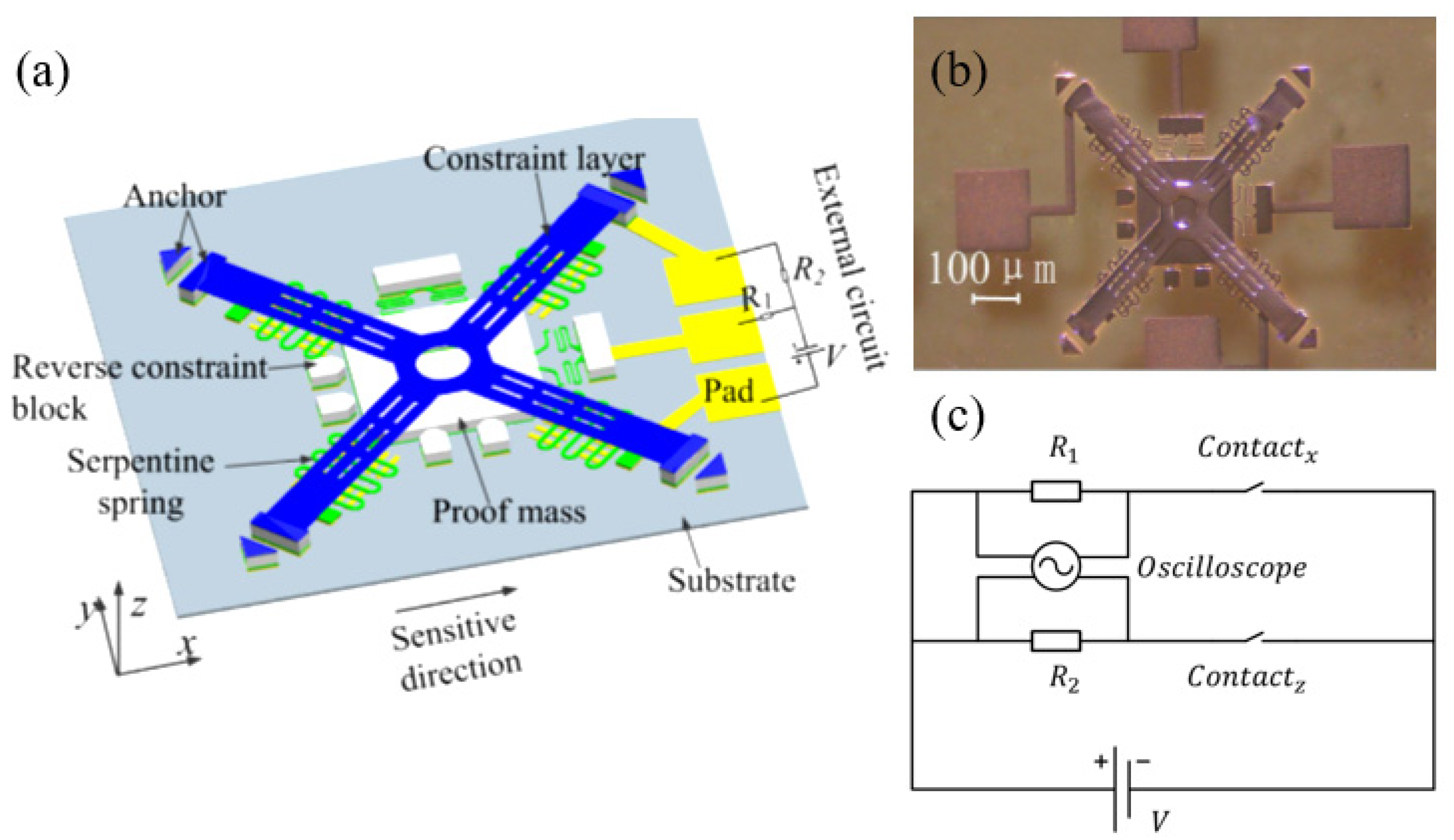
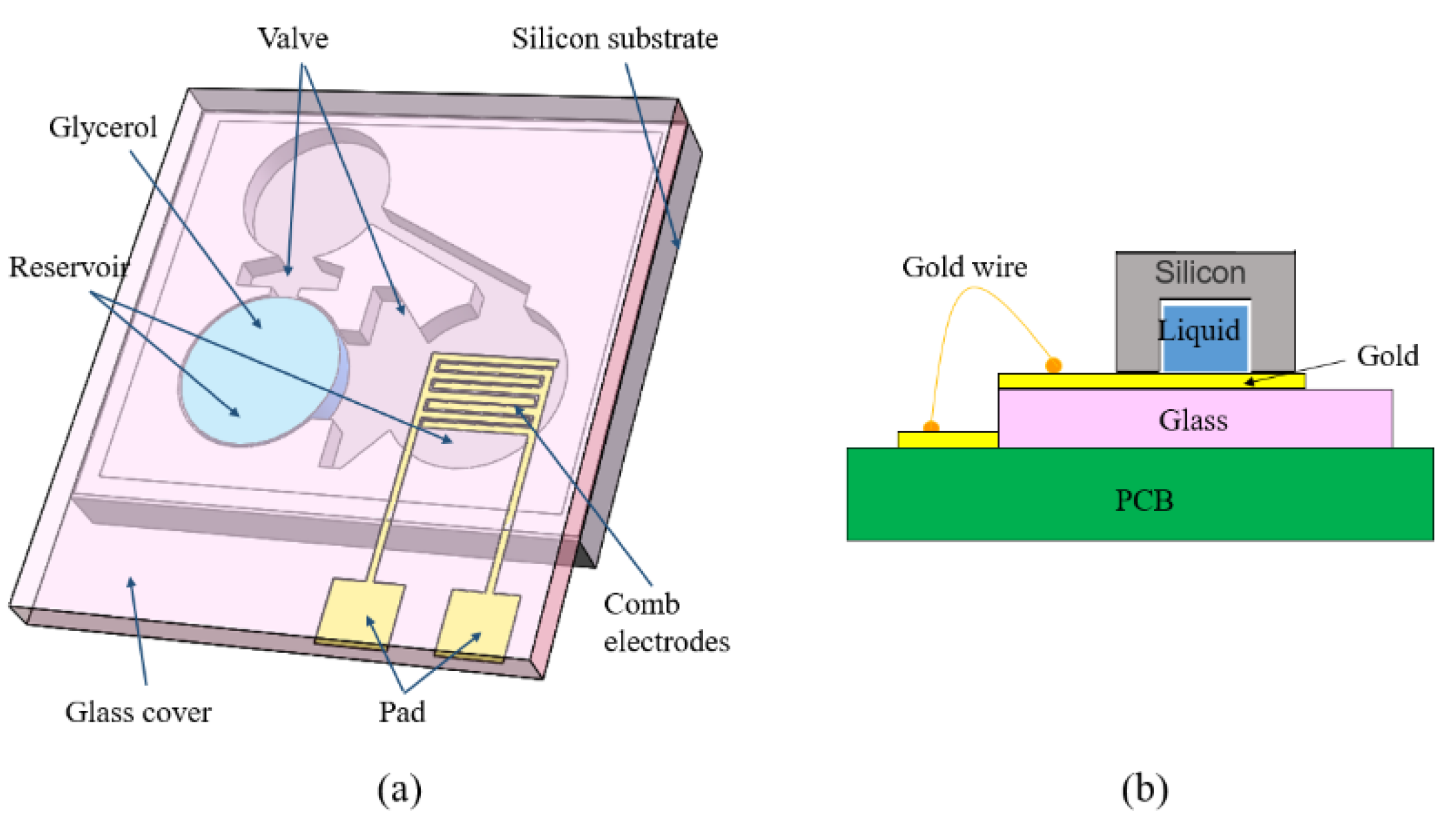
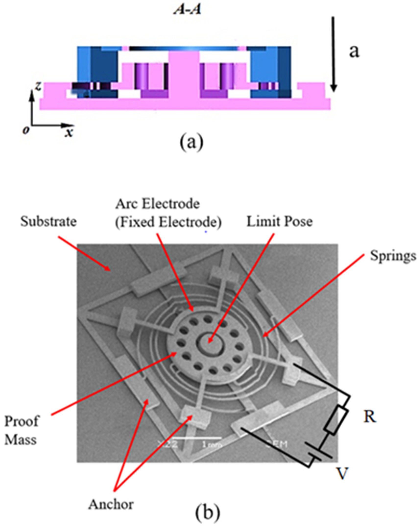
3.1. Passive Inertial Switches

MEMS inertial switches are special acceleration sensors used to detect the threshold acceleration [69]. The microinertial switch based on MEMS technique is generally designed with a flat plate structure, which is characterized by miniaturization, high reliability and a low cost.
Under the premise that the gas damping and structural damping cannot be ignored in the dynamic response, the basic model of inertial switches can be simplified as a spring-mass -damping system, as shown in Figure 1a. When the acceleration applied in the sensitive direction of the switch is at or above the threshold level, the movable electrode moves along the sensitive direction until the relative displacement reaches the distance d between the two electrodes, and the movable electrode contacts with the fixed electrodes to turn the switch on.
In this process, the equation of motion of the mass block can be described as:
m x ¨ + c x ˙ + k x = m a
where m, c, and k are the weight of the proof mass, the damping coefficient and the elasticity coefficient of the movable electrode, respectively. x is the relative displacement between the moving electrode and the fixed electrode, and a represents the acceleration exerted by the outside world on the switch. Inertial switches are discussed below from the aspects of acceleration threshold and contact effect.
Most inertial switches are passive devices, but sometimes switches are designed to be active in order to regulate the threshold. Younis et al. [70] tested two commercial capacitive inertial switches fabricated by Sentasa Technologies [71] (see Figure 1b). The test results showed that the acceleration threshold is linear with the DC voltage for the tunable threshold-acceleration switch. Besides meeting the function of tunable threshold, this kind of switches also have shortcomings: increased volume and power consumption due to added power supply and vulnerability to external electromagnetic interference. Therefore, the passive acceleration switch still plays an irreplaceable role in some applications.
For different application requirements, uniaxial switches [72,73,74,75], biaxial switches [76,77,78], tri-axial switches [79,80] gradually appeared. In the development of MEMS switches, not only the number of acceleration directions have been expanded, but also the axial sensitivity of the switch has been improved [80]. For instance, Currano et al. [81] proposed a triaxial inertial switch based on the symmetrical spiral springs, in which five switches are integrated. In 2014, Chen et al. [80,82] designed and fabricated an all-metal triaxial inertia switch. A triaxial inertial switch can be used instead of multiple uniaxial inertial switches to monitor acceleration in multiple directions and avoid complex installations.
The inertial switch can be divided into high-g inertial switches and low-g inertial switches according to the different load environment applied. On the one hand, the high-g inertial switches generally refer to the inertial switches whose threshold acceleration range is from several hundred g to tens of thousands g. The high-g inertial switches are mainly applied in the harsh environment of high load and high impact, such as in the military. A high-g switch also needs to have better anti-jamming ability and impact resistance. Non-silicon surface machining technology is often adopted in inertial switches. The structure materials and substrates with high strength are used to prevent fracture failure and disengagement of bond wires. Xu et al. [83] developed a multi-directional MEMS inertial switch with shock-resistance. It can resist ultra-high g acceleration (about 100,000 g) in the reverse sensitive direction. The schematic diagram is shown in Figure 2. The design of the constraint structures can prevent false trigger caused by the rebound of the proof mass. Moreover, the insulating quartz substrate is beneficial to improve the impact resistance and thermal stability under ultra-high g acceleration. The proposed MEMS switch is expected to be installed in devices in Internet of Things systems (IoT) to monitor shock and vibration from the external environment. On the other, low-g inertial switches, widely used in the aviation and automotive industries, have acceleration responses ranging from several milli g to hundreds of g. Based on a feasibility study, Lior et al. [84] proposed an idea of using a pair of bistable beams to suspend the proof mass and to sense the acceleration, in which the switch can be closed under sub-g inertias. Nam Lee et al. [85] have developed an inertial switch with a threshold acceleration of no more than 10 g, and it can withstand unexpected shocks of up to 1000 g, making it suitable for harsh military environments.
Rigid electrodes of MEMS switches have the problems of short contact time and signal bounce. To improve contact stability, many methods have been proposed in terms of structure design and materials selection. Huang et al. [6] proposed a time-delay MEMS switch for safety and arming system. As shown in Figure 3, when the acceleration reaches or exceeds the predicted threshold, the working fluid will flow toward the induction reservoir through the capillary valve. After the delay time, the capacitance between electrodes changes and the switch is turned on. The measurements show that the designed switch can realize a delay time of 4.1~10.9 s. Because of the wedge-shaped channel design, it is difficult for the droplet to flow back from the induction reservoir, so the switch can output a stable switch-on signal. This microfluidic switch has simple preparation technology and high reliability, but the working temperature range of glycerol is narrow (−17.8–290 °C). Liu et al. [86], Yoo et al. [5], Li et al. [7] also designed micro-fluid inertial switches based on the principle of inertial flow. They used mercury or an ultra-low temperature conductive fluid as working fluids. Among them, mercury has excellent electrical conductivity, but it is volatile and only suitable for low-g value environments. Liquid metal switches greatly enhance the contact effect, but the choice of working fluids and how to maintain their state stability are tricky issues.
In another way, during the contact process, the deformation of the flexible electrodes (i.e., the fixed electrode or the movable electrode) can provide a buffer for the collision contact between the electrodes, so as to prolong the contact time. Du [8] developed an inertial switch with a low stiffness-fixed electrode for extending the contact duration in 2020 (see Figure 4). The fixed electrode was designed in an arc to reduce its stiffness. The inertial switch was fabricated by UV-LIGA, in which the method of width compensation was adopted to improve the fabrication accuracy. The result showed that the contact time can reach 260 μs when the designed switch is triggered by 32 g. At the same time, Xu et al. [87] proposed a vertically driven MEMS inertial switch with a flexible structure. The designed switch can achieve 125 μs contact time at 288 g acceleration. By contrast experiment, the conclusion has been proved that the extension of contact time can be achieved by reducing the stiffness of the fixed electrode, especially its thickness.
In addition to the method of utilizing flexible structure to extend the contact time as described above, some literature mentioned carbon on nanotubes (CNTs) as electrode contact materials [9,88,89]. CNTs are suitable for use as contact materials due to their excellent mechanical and electrical properties. Lee et al. [9] have fabricated an inertial switch with CNTs-to-CNTs contact. When the moving electrode collides with the fixed electrode, the elastic deformation of the CNTS greatly increases the contact time. The results showed that under the same conditions, the contact time of the CNTs-based switch was 114 μs, while that of the switch without CNTs was 7.5 μs. Its lifetime is tested to be longer than 57 thousand cycles. The electrothermal actuator and bistable mechanism are used to form the initial gap between electrodes.
Further, there are also some methods taking advantage of the latching mechanism to maintain the switch-on state. The common methods include the mechanical locking mechanism and the bistable mechanism. Mechanical locking switches utilize a pair of mechanical locks to buckle electrodes together [90,91]. The design of the mechanical locking switch requires consideration of an unlocking mechanism to release the movable electrode, without which the switch will remain on after being triggered. The design criteria of bistable bending beams can be found in [92,93]. Zhao et al. [94] developed a bistable inertial switch based on the structure of an inclined buckling beam. Go et al. [95] fabricated a bistable inertial switch using a SiO2/p+-Si bimorph with residual stress. Frangi et al. [96] also developed a similar bistable structure. These switches require to be applied to the opposite force to restore themselves to the original position. It is worth mentioning that apart from being widely used in inertial switches, the latch mechanism is often used in a variety of other switches to reduce power consumption and enhance switch closure, as described in the following sections.

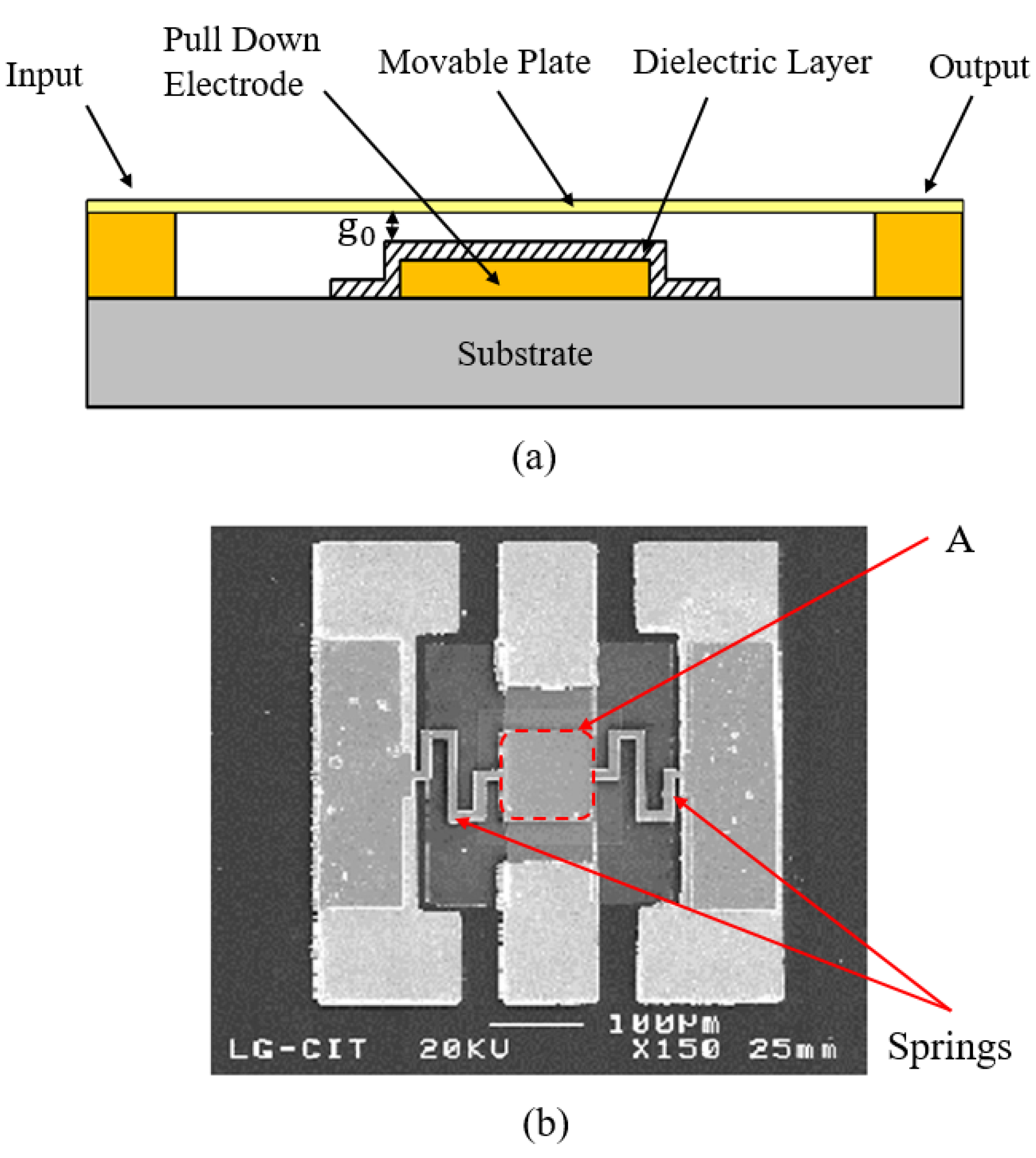
3.2. Electrostatic Switches

The principle of electrostatic actuation widely used in MEMS is the utilization of electrostatic attraction between charged objects to cause the deformation or displacement of objects. Electrostatic switches have been widely studied, and long-term reliability is the main problem that restricts their development. The experiments conducted by G Goldsmith [97] show that the lifetime of the capacitive switch is exponentially related to actuation voltage. For every 5–7 V reduction in the actuation voltage, the switch lifetime is extended by 10 years. Reducing actuation voltage not only extends switch lifetime, but also facilitates its use in wireless devices [98].
The schematic of a generic switch with electrostatic actuation is shown in Figure 5a. For electrostatically actuated switches, the Coulomb force is proportional to the applied voltage. When the Coulomb force exceeds the elastic restoring force of the movable electrode, it suddenly collapses onto the fixed electrode. This phenomenon is called pull-in instability [99] and the corresponding potential difference, which is a critical value, is called the pull-in voltage. The thin dielectric layer exists to form a coupling capacitor between the electrodes [100]. When the two come into contact, the coupling capacitance becomes so large that the switch is turned off. In order to obtain a large on/off capacitance ratio, the dielectric layer is usually made very thin (not exceeding 300 nm), while capacitive switches typically require 30–80 V. At this high field intensity, charge trapping is prone to occur, which causes the dielectric layer charging [101]. The accumulation of charging charges will eventually prevent the plate from being pulled down or cause the plate to adhere to the dielectric layer, resulting in switch failure. The reliability of the capacitive switch can be improved by optimizing dielectric materials and decrease the driving voltage. Equation (2) gives a widely cited formula for calculating the pull-in voltage of a vertically driven capacitor switch with a traditional rigid plate:
V p = 8 K g 0 3 27 ε 0 A
where K is the spring constant of the moving structure in the desired direction of motion, g 0 is the initial gap between electrodes, ε 0 is the dielectric constant, and A is the area applied to the movable electrode. The equation intuitively shows the influence factors of actuation voltage. Reducing the spring constant K has been shown to be the most effective way to reduce the voltage structurally and subsequently prolong the switching time [102]. Figure 5b is a RF MEMS capacitive switch fabricated by J.Y.Park et al. [10]. Strontium titanate oxide (SrTiO3) with a high dielectric constant is used as the dielectric layer. In order to reduce the actuation voltage, comparative experiments have been carried out from the aspects of spring geometries, transmission line surface materials and initial gap height. The experimental results showed that the switch with serpentine springs has the lowest actuation voltage (i.e., 8 V) through reducing the spring constant without taking up too much space. This RF switch can be widely used in wireless applications.
It should be noted that unlike the rigid plates mentioned above, the research on elastic plates has been on the rise in recent years. For instance, micro-curved plates can exhibit bistable behavior under appropriate driving force [103]. Although it is difficult to fabricate curved bistable microplates in the MEMS process, it is still a promising research direction. For instance, Asher et al. [104] presented a self-molding forming technique for extruding non-planar thin-walled microstructures with a soft foam stamp. The bistable microcap was fabricated and its bistability was verified for the first time. A similar fabrication method can be found in [105]. Compared with the rigid flat plate, the bistable curved plate used in the switch has the features of reducing power consumption, improving response speed and increasing output displacement. The design method of bistable curved circular plates driven by electrostatic force can be found in [106,107] to determine the initial geometric parameters.
The structure of a capacitance switch is simple, but the displacement range is limited by the nonlinear behavior of electrostatic force. In order to extend the stable stroke of the electrostatic drive (≥10 μm), the comb-like actuator is usually used. Electrostatic comb-driven switches are laterally actuated [108] and their contact modes are generally designed to be resistive. In some case, the output force is independent of displacement. Almeida et al. [39] fabricated a comb-like electrostatic multi-contactor RF MEMS switch which can be simplified, as shown in Figure 6a. The switch consists of a movable main beam, five movable fingers and six fixed fingers. When a DC voltage is applied to one of the comb-drive actuators, the main beam is moved by electrostatic force, causing movable fingers to come into contact with fixed fingers (see Figure 6b). Au was electroplated on the contact surface to reduce the contact resistance. The overall size of the switch is 3 × 3 mm² and the initial gap between electrodes is 10 μm. However, the comb-like structure of the proposed device makes the actuation voltage increase up to 172–220 V, which not only limits its integration with the IC, but also easily leads to adhesion between electrodes [109]. The lifetime of this switch was tested up to 80,000 cycles.
The optimization of electrostatic MEMS switches is mainly achieved by reducing its actuation voltage [110]. Current methods include shape optimization of comb fingers [111], reduction of the driven gap [112] and reduction of the spring constant [102]. Park et al. [113] proposed a laterally capacitive shunt MEMS switch fabricated on an SOI (silicon-on-insulator) wafer. One thousand comb fingers were used with a gap of 2.1 μm. The air was used as both on and off state capacitive coupling switches instead of dielectric material. The actuation voltage of this switch is 25 V. The second way is the reduction of the spring constant. Kundu [12] reported an RF MEMS switch with low actuation voltage. The actuation voltage was reduced from 20 V to 15 V by introducing the concept of a moving bottom plate and analyzing the performance characteristics of such MEMS switches with two movable plates. Chu [114] proposed a method to realize low voltage of electrostatic switches by utilizing the buckling and bending effects caused by residual stress. The minimum voltage of this switch is 10.2 V. Agrawal et al. [115] presented an electrostatically actuated switch with a hollow beam. By comparing it to the switch with solid beam structure, it was found that the driving voltage of the hollow-beam switch was reduced by four times and the chip area was not increased.
The bistable mechanism can be used to reduce the voltage and power consumption of electrostatic switches. For a traditional electrostatic-driven bistable structure, the switching of two ground states generally requires two driving electrodes to apply two opposite loads on the bistable structure [116,117,118], thus increasing the chip area. Kwon et al. [119] proposed a spatula-shaped comb actuator to realize the bistable state of the bending beam. The direction of the electrostatic force can be changed by changing the relative position of the movable comb and the fixed comb. This design only requires a single driver electrode, but the overall size is not reduced. In recent years, it has been found that dynamic snap-back can be used to release a latched beam with a single electrode [120], which can reduce the chip area. The principle is to apply a gradually increasing voltage to the bistable beam until the voltage is slightly higher than the pull-in voltage, then suddenly remove it. The beam will return from the latched state to its original state. In addition to the lateral drive, Medina et al. [121] later applied this concept to the out-of-plane actuation and presented a snap-through switch actuated by a bistable bow-like beam. Its bistable structure helps to reduce power consumption. The use of the bow-beam actuator reduces the voltage by 45% compared to the common snap-through switch. Furthermore, the research of a capacitive cantilever beam switch driven by three steady-state electrostatic forces has appeared recently [122]. Symmetry breaking should be paid attention to in the design of a bistable structure [93,123,124]. When the ratio of arch height to arch thickness is greater than a certain value, asymmetric transition will occur, which is a hindrance to the realization of latching.
For comb drive electrostatic switches, there is also a signal partition problem that must be paid attention, namely drive signal and switch signal non-interference. Kang et al. [125] introduced a change in the fabrication process of a comb-driven RF MEMS switch. For this device, a 2 μm thick layer of tetraethyl orthosilicate is deposited and then patterned on the silicon structural layer. The signal pads are then made and contactors coated by electroplating 3 μm Au. In this way, an isolation is formed between the electrostatic drive signal and the on–off signal of the switch.

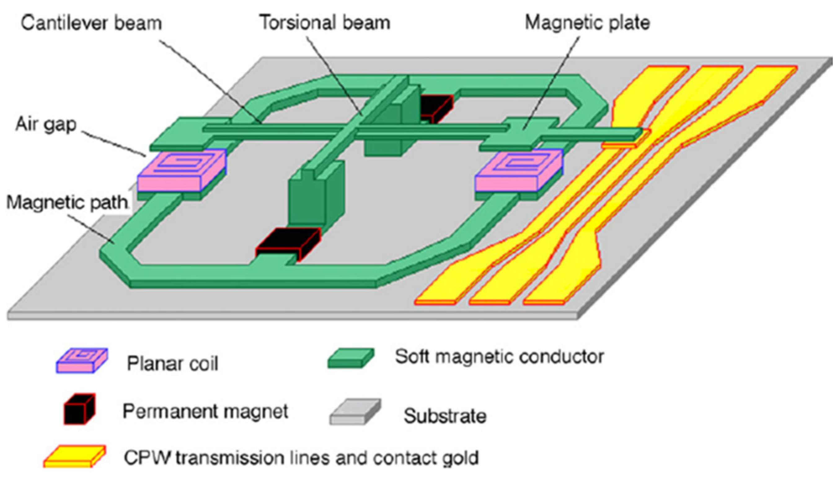
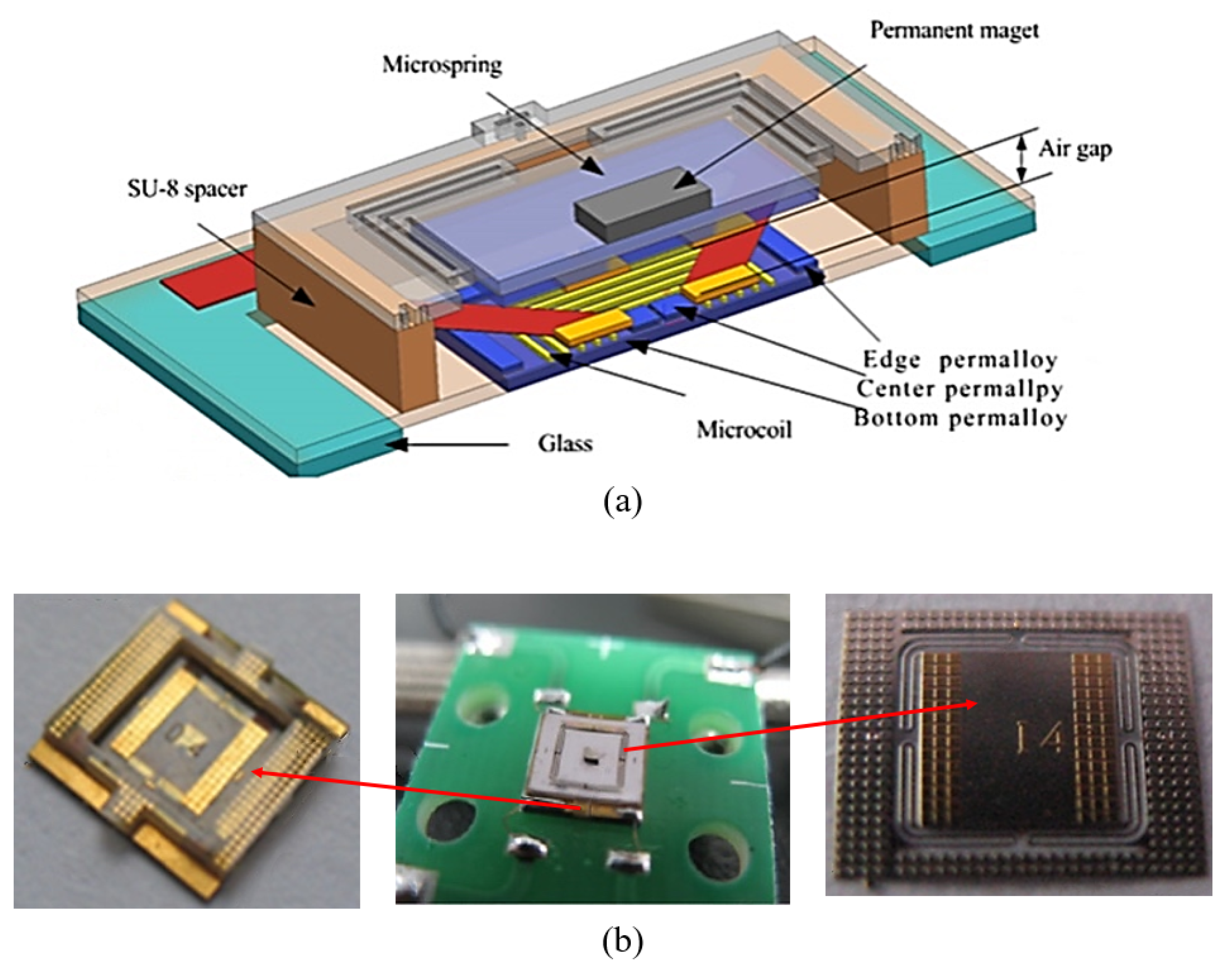
3.3. Electromagnetic Switch

The principle of the electromagnetic micro-switch is that the magnetic movable electrode attracted by the electromagnetic coils moves to the substrate, and then the contacts are sucked together and the controlled circuit is switched on [126]. The state conversion of the switch is achieved by entering a bidirectional DC pulse current into the coils.
In 2007, Zhang [127] reported a high-speed bistable electromagnetic actuator for resistive RF MEMS switches by UV-LIGA technology. A schematic drawing of the electromagnetic actuator is shown in Figure 7. There are many details that can be enhanced in order to improve performance. The application of a torsion beam can improve the restoring force and reliability of the cantilever beam. Quartz glass was chosen as the substrate material here to reduce the substrate power loss. The cantilever beam with a T-shaped cross-section was adopted for larger displacement and reduced mass of the device. The multilevel Cu coils were designed in plane structures to adapt to the MEMS process. Al 3 O 2 was sputtered as the insulating layer. The permanent magnets made by precision-machining technology are manually installed into the device. The test results showed that the switch speed is 20 μs at 50 mA pulse current. Under the action of the torsion beam and permanent magnet, a bistable state can be easily realized, thus reducing power consumption. The overall size is 2 mm × 2 mm.
Miao et al. [128] proposed an electromagnetic bistable switch by surface micromaching technology on a glass substrate, as shown in Figure 8. In their ingenious design, the switch mainly consists of a coil component and a spring supporting a permanent magnet. The switching of the two steady states is realized by changing the direction of the pulse current in the coil. The top and bottom contactors are made of electroplated Au. By adjusting the width and thickness of the cantilever beams, the spring elasticity can be increased in a limited space, thus reducing the actuation voltage. Polyimide is used to prepare insulating layers. At 5 V pulse voltage, the switch can achieve a response time of no more than 5 ms and an output displacement of up to 380 μm. Unfortunately, this form of microassembly increases the difficulty of operation, and the complex process of the electromagnetic MEMS switch limits its mass production. The chip area of the switch is 6 mm × 6 mm.
A l 2 O 3 and polyimide are often used as insulators in electromagnetic MEMS switches. The structure of microcoils has a direct influence on performance of the switch [89], for example, multi-layer coils and the addition of magnetic cores can significantly improve the driving force. A permanent magnet allows the electrodes to remain in contact after the current is removed without additional power apply, through which the switch can achieve a bistable state to reduce power consumption. The actuation voltage of electromagnetic switches is as low as the requirement of the integrated circuit (<10 V), and the switch has fast response speed (<5 ms). It can adapt to a bad environment [128], especially suitable for large displacement (50–400 μm) [70]. The deficiencies of these switches are complex process (some require microassembly) and need to occupy a large chip area (>2000 × 2000 μm2). Electromagnetic switches have not advanced by leaps and bounds in the last decade. To greatly improve the applicability of electromagnetic switches, future optimizations should still focus on reducing the power consumption, reducing the size without reducing the electromagnetic force and improving the maturity of the processing technology.

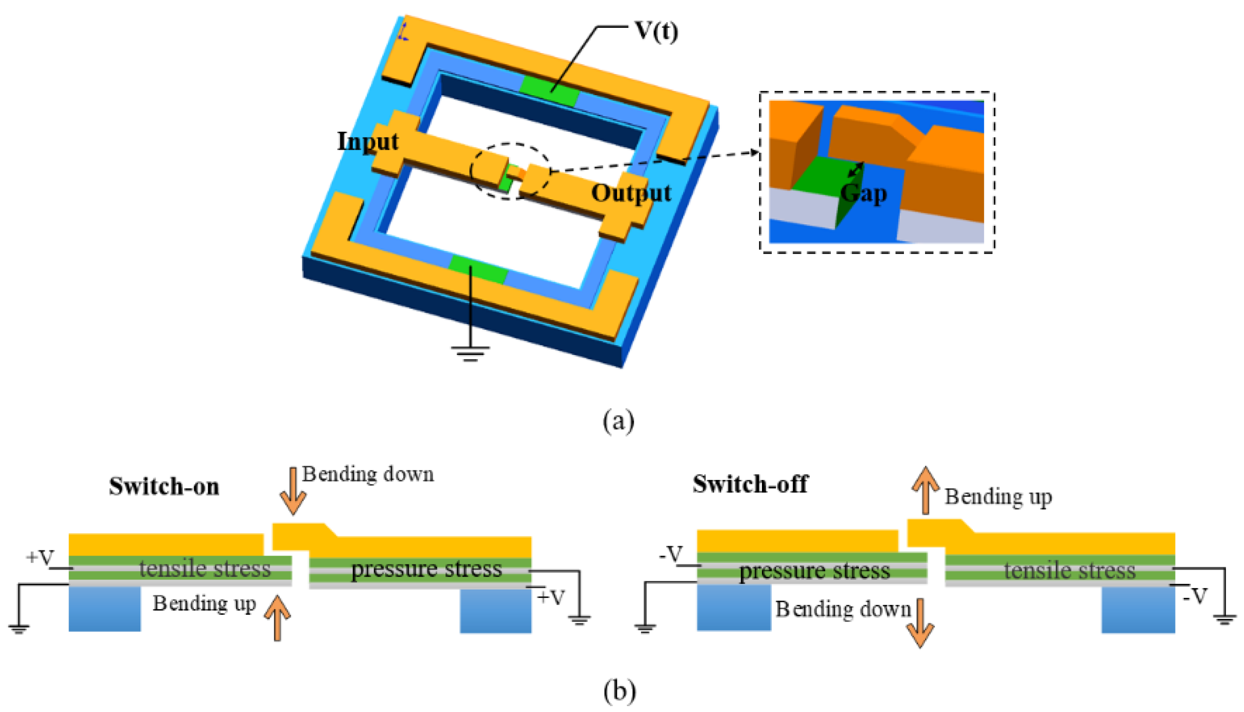
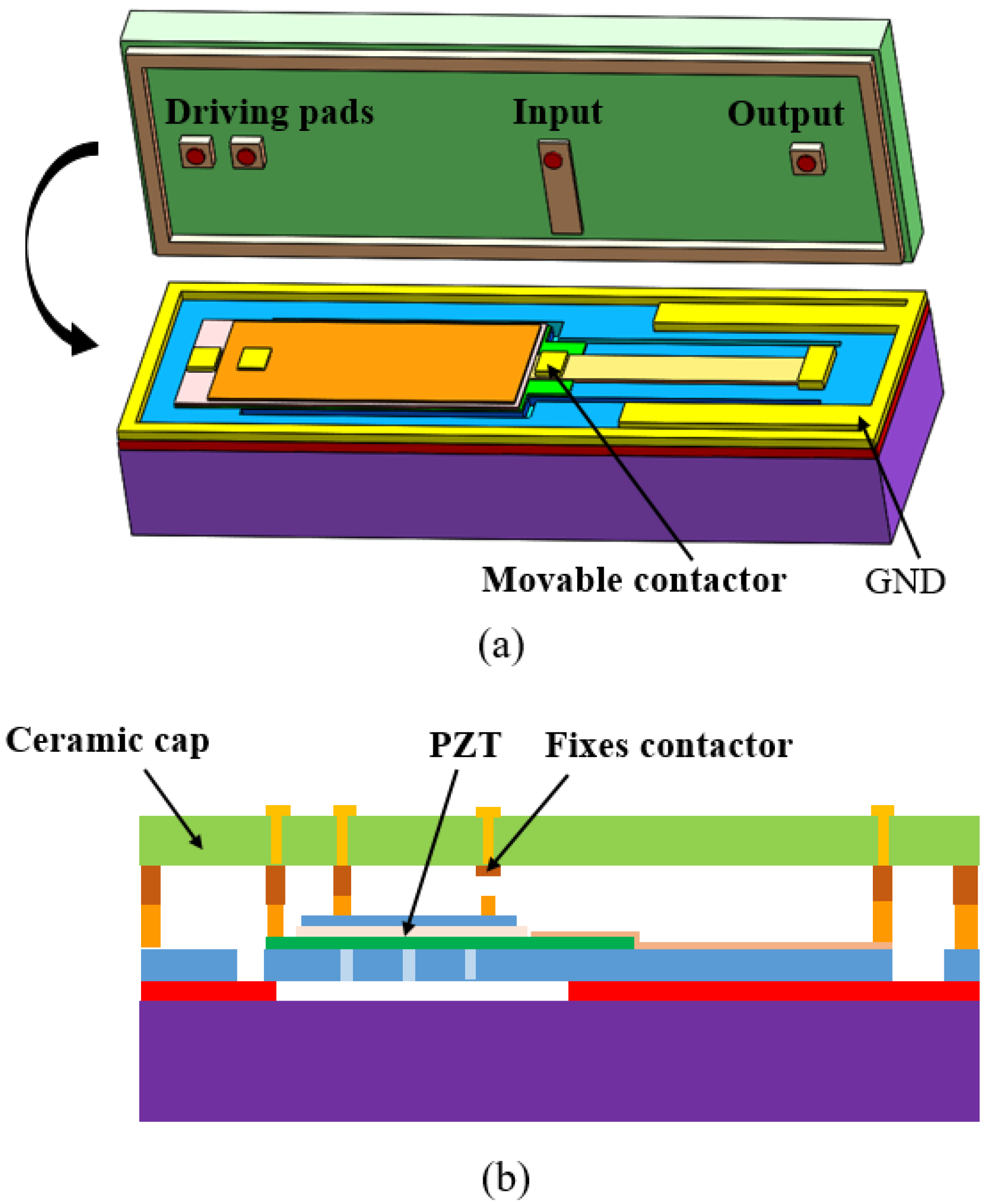
3.4. Piezoelectric Switch

As for piezoelectric switches, switching between on and off is achieved by the converse piezoelectric effect of piezoelectric materials [129]. Piezoelectric strains can be either positive or negative, therefore this kind of switch can be used actively to turn the switch off as well as on. Widely used piezoelectric materials include aluminum nitride (AlN), lead zirconate titanate (PZT) and so on.
R. Mahameed et al. [11] firstly proposed a laminated double-beam RF MEMS switch based on AlN (see Figure 9). Compared with PZT, the fabrication process of AlN is compatible with a CMOS (complementary metal-oxide-semiconductor transistor). The dual-beam design is adopted to essentially compensate for the residual stress in the deposited films, where the bottom layer of AlN is used for driving. The switch can be used actively to turn the switch off as well as on by reversing the polarity of driven voltage. The drive pads are utilized to drive both beams at the same time. In this way, the drive voltage is reduced to no more than 20 V, the contact force doubled, and the switching time reduced by half.
Nakatani et al. [130] developed a compact resistive piezoelectric actuated switch, as shown in Figure 10. The silicon beam of the switch was fabricated by opening a window on the device layer of the SOI wafer and then etching the buried silicon dioxide layer with hydrofluoric acid. The PZT film actuator and movable electrode were in turn prepared on the device layer. The ceramic cover plate with a fixed electrode was finally bonded to the SOI wafer to form the initial gap and tightly package the switch at the same time. In the initial state, the uniform 0.5 μm gap between the electrodes makes the structure compact. The fabricated switch can produce a contact force of 1 mN at a driving voltage of 20 V. In this way, the high restoring forces prevent adhesion, and this sealing solution prevents also the organic contamination of the contact surface. These design details help to make the service life of the switch up to 1 billion.
The well-known bistable mechanism is also used in piezoelectric actuation. Manuel Dorfmeister et al. [131] proposed a piezoelectric actuator with a bistable membrane. An SOI wafer with a 2 μm thick device layer was used as the substrate and the AlN layer was deposited as the piezoelectric layer. Si 3 N 4 was sandwiched between them as the insulating layer. When the internal stress exceeds the critical value, the film will deflect and remain in its stable state. The film can be converted between two ground states by applying impulse currents in reverse. The AlN bistable piezoelectric film produced a displacement of 10 μm. The bistable membrane design is expected to be applied to piezoelectric MEMS switches to reduce power consumption.
Piezoelectric drive has the advantages of fast response speed (<300 μs) [11] and stable output, even for small displacements (0.5–2 μm). Piezoelectric actuation is the most suitable technique for the biomedical devices of all actuation types [132]. PZT has a high value of the piezoelectric coefficient d33 > 100 pC/N, while this of AIN is d33 = 5 pC/N, so PZT is most commonly used in the research of piezoelectric switches. In order to reduce the power consumption of piezoelectric switches, bistable mechanisms such as bistable curved microplates can be adopted [133]. The fabrication of piezoelectric materials by the MEMS process is a concern.

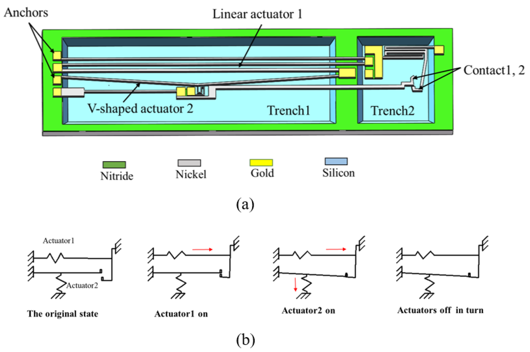
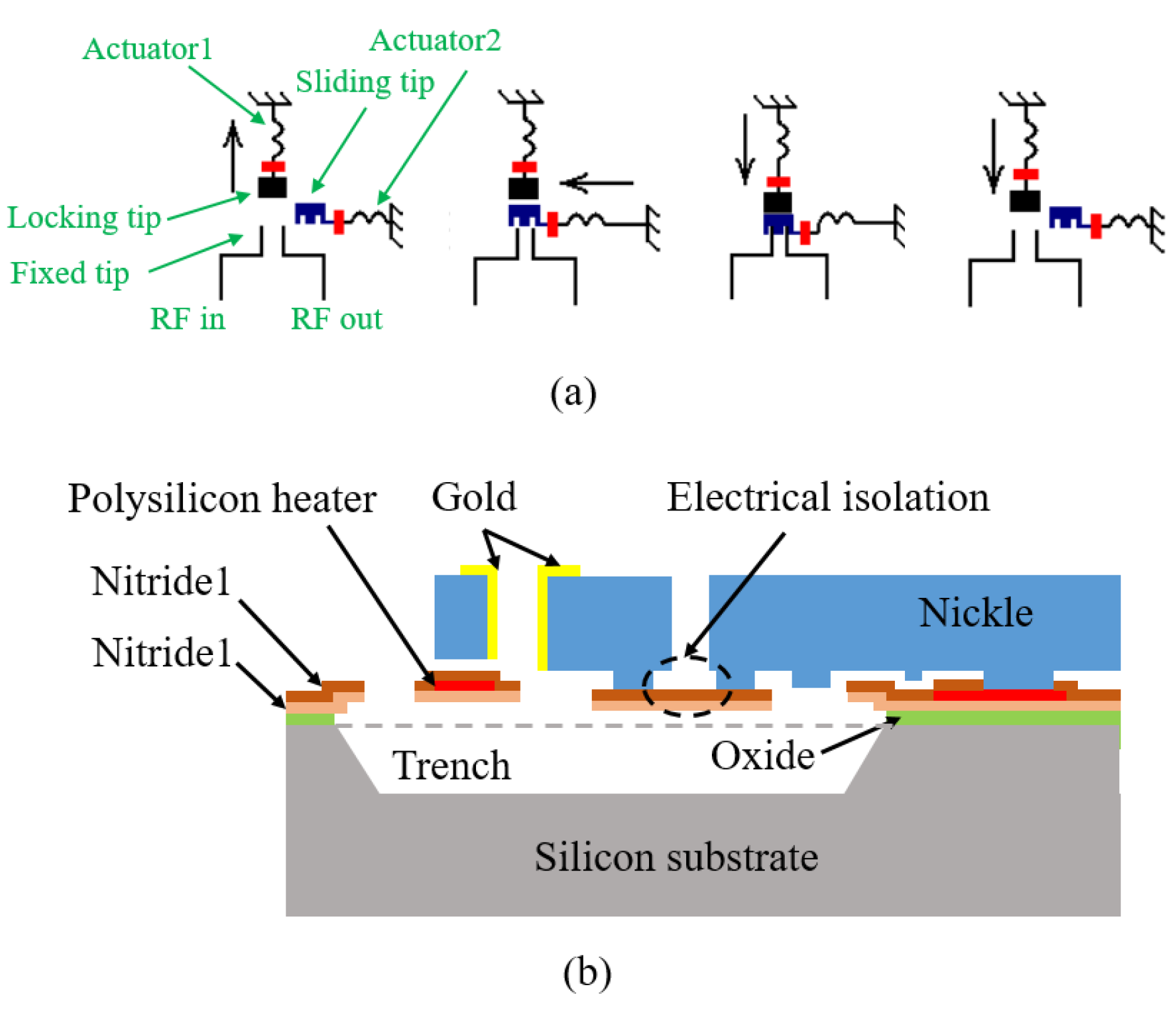
3.5. Electrothermal Switch

The common thermal-actuated structures are the bimorph structure and bending beam structure (including V-shaped and U-shaped beams). The principle of the bimorph actuator is similar to that of piezoelectric actuators [134,135]. Electrothermal switches based on bending beam actuators, especially V-shaped actuators, have been studied extensively.
Dellaert D et al. [40] proposed a compact thermal driven latched MEMS switch, as shown in Figure 11. The main structure of the switch is composed of a linear actuator, a V-shaped actuator, a pair of vertically placed contacts and two levers. The two actuators drive the contactors respectively, and the contactors realize a bistable state by means of mechanical self-locking. The levers are used to slightly amplify the displacement. The combination of the two actuators makes the switch produce a high execution force of 1.33 mN at a small displacement. The use of MetalMUMPs (metal multi-user MEMS processes) technology allows the patterned S i 3 N 4 layer to be suspended on the etched trench and to support the 20-μm nickel structure layer. In addition to mechanical support, the silicon nitride layer acts as an insulator to separate the drive current from the switch signal. Au is sputtering on the sidewall of the contactors to lower the contact resistance, which is 0.6 Ω at 10 mA. The prominent features of the switch are to save the chip area through reasonable placement and to reduce the contact resistance through using a metal structure, sputtering Au on the sidewall of the contacts as well as high contact force of 1.33 mN at the switch area of 2020 × 330 μm².
Bakrikassem, M. et al. [41,42] proposed an electrothermal mechanical latching switch. Its working principle is shown in Figure 12a. The switch closure and latch are realized through the sequential actions of two sets of electrothermal actuators. The switch is fabricated using the MetalMUMPS process, as shown in Figure 12b. The polysilicon layer acts as a heating resistor. When a current is applied to the polysilicon resistor through the DC pads, the heat generated is transferred to the V-shaped metal actuator structure through the Si 3 N 4 layer that wraps it. When the groove on the sliding tip moves to the top of the fixed tips, the latch tip presses the sliding tip down by restoring force and latches the position. The sliding tip acts as a bridge connecting the two fixed tips and closing the circuit. On the one hand, Si 3 N 4 protects polysilicon from corrosion by KOH solution used to etch the trench; on the other hand, it separates the drive signal from the switch signal to avoid signal coupling (between the locking tip and the actuator, and between the sliding end and the actuator). The reaction force on the sliding tip produces vertical strain inside the locking tip, which affects the service life of the Si s N 4 layer below the locking layer. The actuator is fabricated by 20 μm thick Ni connected with an Au-plated tip to enhance the contact effect. The DC power consumption is 250 mW for a displacement of 32 μm in 14 ms.
Zolfaghari P et al. [13] have studied a kind of electrothermally driven bistable RF MEMS switch with low power consumption, as shown in Figure 13. The MetalMUMPs technology was also adopted and the structure layer was made of Ni. The switch structure has a symmetrical distribution, with U-shaped actuators linked with movable contacts on either hand and a V-shaped actuator with a movable contactor on the top. The S i 3 N 4 layer not only connects the contactors to the U-shaped actuators or the V-shaped actuator, but also insulates the drive signal from the switch signal. U-shaped actuators are used to pull apart the two lower contactors, and V-shaped actuators are used to push the upper contactor forward. Pulse voltages are applied sequentially to the U-shaped and V-shaped actuators, and the switch can be on or off. When the sidewall of the three wedge-shaped contacts fit together, the mechanical forces they generate latch the position of the switch. Au film of 1–3 μm is deposited on the surface of the contactors by electroplating to reduce contact resistance. The driving voltages are no more than 1 V, and the contact resistance is 0.028 Ω.
There are also some structural variants of actuators for electrothermal switches. For instance, Kim et al. [136] proposed an actuator with stepped beams fabricated on an SOI wafer in 2013 (see Figure 14). When current is applied from the anchors of the beam array, the difference in section thickness of the beams causes a bending motion in the vertical direction. This actuator can be used for vertically actuated switches.
The thermal actuation overcomes the weakness of a great dependence on the gap compared with electrostatic and electromagnetic actuation, and has large output displacement (laterally actuated >30 μm) [137] and output force (>500 μN) [138]. The main disadvantages of thermal switches are slow response (a few thousand μs) and high power consumption (a few hundred mW). A great deal of effort has been made to address the shortcomings of electrothermal switches. Similar to switches with other driving principles, bistable systems are frequently used for their low power consumption [13,40,41,42,139,140]. The response speed of MEMS switches can be improved by the actuator optimization of geometry, material properties and driven voltage. Electrothermal switches are basically resistive switches. Thus, low contact resistance is the key performance of this type of switches. In the switch fabricated by MetalMUMPS process, 2–3 μm Au layers can be electroplated by sputtering the seed layer first. Alternatively, in the case of SOI wafers, the non-perpendicularity of sputtering can be used to sputter the Au directly on the contact surface of the structural layer. Oh C [141] mentioned that: firstly, the sample is fixed and the contact surface on one side is sputtered Au, and then the side wall of the other contact surface is coated by rotating the sample 180° along the normal direction of the substrate. In this way, the metal layer sputtering of the two contact surfaces can be better realized. Signal interference occurs if the drive signal and the switch signal are not isolated. Generally, an electrical isolation layer is sandwiched between two layers of the driving structure and contact. The electric isolation layer is usually the Si 3 N 4 layer [40,41], or the SiO 2 layer which is formed by plasma-enhanced chemical vapor deposition (PECVD) [142] and then patterned.

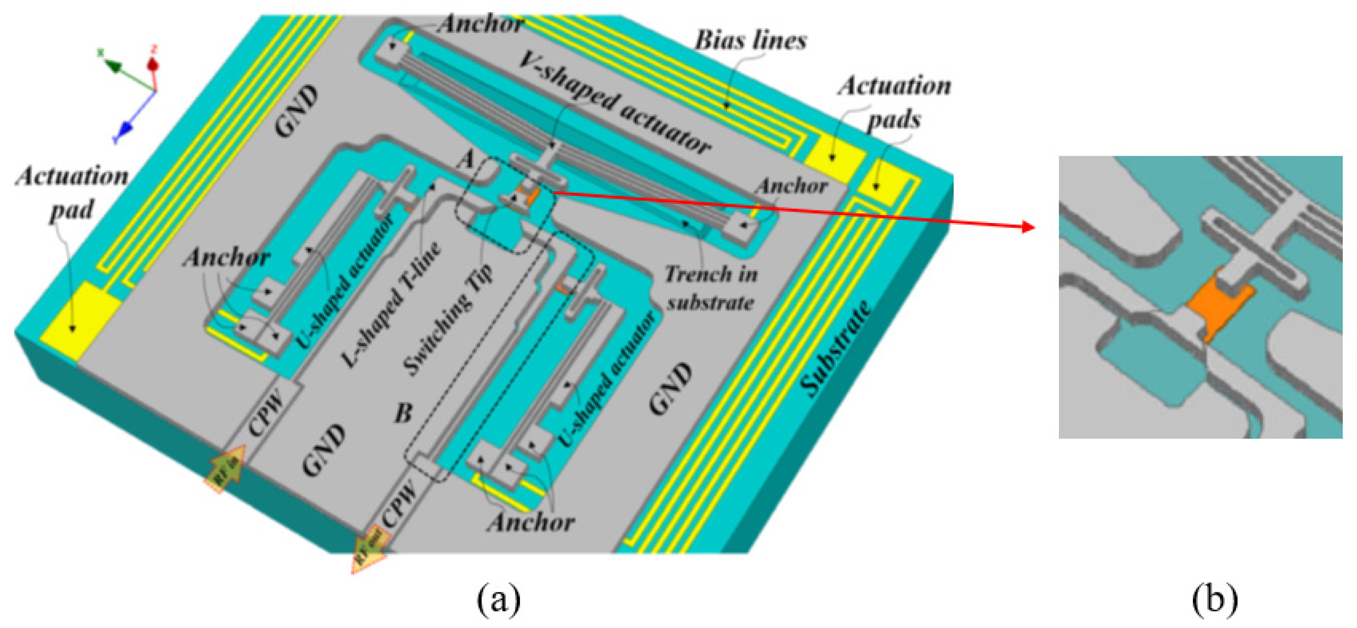
3.6. Multiple-Actuation Switch

All of the above drive switches have their advantages and disadvantages. For example, the electrostatic drive consumes extremely low power and has a simple fabrication process, but the electrostatic actuation requires 20–100 V or even higher driving voltage, which is not conducive to system integration and long-term reliability. Thermal actuation and electromagnetic actuation can generate greater force and output displacement than electrostatic actuation, and the required voltage generally does not exceed 10 V. However, continuous power supply results in large power consumption. In this case, various improvements have been discussed, including reducing the voltage of the electrostatic drive, increasing the switching speed and the displacement of the capacitor switch by employing a bistable film, and reducing the power consumption of the electrothermal and electromagnetic actuation by latching mechanisms. In addition to these, there are some efforts to combine multiple drivers and leverage their strengths while avoiding their weaknesses.
Cho [143] reported a MEMS switch that combines electrostatic and electromagnetic actuations, which means using electromagnetic force for switching and electrostatic force for state retention. Driven by the electromagnetic force, the displacement is linearly related to the applied current. The initial gap of the two contacts is 10 μm, the driving voltage is 2 V and the holding voltage is 3.7 V. The transient response indicates that the switching time from off to on is less than 110 μs, while the switching time from on to off is about less than 380 μs. The power consumption is only 40.3 μJ. Chae et al. [144] proposed an RF MEMS switch that takes advantages of electrostatic and electrothermal drives. The driving voltage is 0.3 V and the holding voltage is 15.4 V. The switching time from off state to on state is 47 μs, while the switching time from on to off is 4.5 μs. The power consumption is 3.24 μJ. Similar work can be found in [144,145,146,147,148]. The actuation voltage and power consumption of these multi-drive switches are both decreased. The downside, of course, is the increased chip area and complexity.

3.7. MOEMS Optical Switch

The MOEMS optical switch is not a kind of conventional MEMS mechanical switch, so this review only mentions it in passing. It is actually a technology of optical path switching employing MEMS components such as movable micromirrors and movable resonators [149,150]. Typical MOEMS optical switches consist of input/output optical fibers, movable micromirrors and actuators. By apply the appropriate driving voltage, the micromirror array can move along a straight line or twist at an angle so as to realize on and off of the optical path. The driving principle of MOEMS optical switches can be electrostatic, electro-thermal or other actuations as mentioned above. For instance, Sun et al. [151] proposed a 2 × 2 electrostatic-driven optical switch with a torsion beam. The upper and lower electrodes form a flat capacitive structure with an electrical isolation layer between the two and a micromirror on the upper electrode. When no voltage is applied, light beams are reflected by the micromirror. When the driving voltage is applied, the upper plate bends, thus changing light beams from a reflected state to a transmitted state. The optical switch is processed by MEMS switch technology, which has the advantages of miniaturization, mass quantization and compatibility with large-scale integrated circuits. It plays an important role in optical fiber communication.

4. The Development Trend of MEMS Switches

For a more intuitive view of the development direction of MEMS switches over the past 20 years, the switches and their characteristics in some representative articles are listed in the following Table 3 in chronological order.
As can be seen from Table 3, passive inertia switches remain a research hotspot benefiting from their particular application market. As for active switches, electrostatic and electrothermal switches have developed more rapidly in recent years. In the choice of contact mode, the resistive switch is the mainstream relative to the capacitive switch. For resistive switches, Au-Au contact is mainly selected from the point of view of reducing contact resistance. Further from the point of view of reliability, there are but few switches using other contact materials. The performance optimization of various switches mainly focuses on the following aspects: (1) Reduced power consumption. Of all, electromagnetic and electrothermal actuation require relatively high power consumption. At present, the main method to reduce power consumption is to use a bistable mechanism due to their ultra-low power consumption, as both ground states remain stable without any energy supply [13,93,95,122]. (2) Enhanced contact performance. For resistive switches, switches need to have good contact effect to accurately identify switch signals. The extension of contact duration can be achieved by decreasing the stiffness of electrodes; utilizing latching mechanisms including mechanical self-locking, a bistable mechanism and a wedge-shaped channel, etc. [4,5,6,7,8,74,77,80]. The contact resistance can be reduced by using the contact materials with low resistivity [13,57] and increasing the contact force [80,165]. (3) Process technology. The current fabrication technologies of MEMS switches are mainly divided into SOI bulk micromachining and metal surface micromachining. The excellent mechanical and electrical properties of metals facilitate the transfer of switch signals, which leads to the wider application of MetalMUMPs technology in the fabrication of MEMS switches [8]. However, silicon-based MEMS switches are also being studied persistently due to their unsurmountable merits, that is, high shape precision and simple and mature processes, which are more suitable for mass production. (4) Impact resistance. This specification, especially for inertial switches, can be met by optimizing the structure and substrate materials [59]. (5) Miniaturization. One of the reasons passive switches stay hot is their smaller size when compared to active inertial switches. The thermal actuator can achieve a large displacement output, but its slender shape takes up a large chip area. Therefore, novel designs tend to be developed to make the structure more compact [80]. (6) Improved durability. The long-term lifetime of MEMS switches has been improved in many ways, such as by adopting dielectric-free switches to avoid dielectric charging, choosing gold alloys or contact materials combining gold with other materials to reduce contact degradation, enhancement of heat dissipation of devices, reducing residual stress in structural design and process technology, and strengthening seals to prevent moisture and pollution.
Through the above analysis, it can be found that MEMS switches are distinguished by miniaturization, low power consumption and intelligence, but there are still some problems that need to be urgently solved. Typical problems include: (1) Complex processing technology. There are manifold MEMS processing steps, and some still need to be manually completed, where subjective error is big and quality consistency is difficult to guarantee. (2) Lower reliability [166]. Reliability is a key performance in switch alignment applications. Due to the repeated use of switches and environmental factors, MEMS switches are prone to failure. Although MEMS switches are increasingly needed in civil and military applications, their reliability is often neglected in design. To date, the related failure modes and mechanisms have not been fully explored. In addition, there is also a lack of unified standards to check the reliability of switches, such as lifetime, mechanical properties and so on. (3) High packaging cost. The packing of the switch has always been a conundrum [167,168]. The packaging cost of switches is often much higher than the manufacturing cost, which restricts their mass quantification.

5. Summary and Outlook

Over the past decades, various MEMS switches have been designed and fabricated. In this paper, the structural characteristics, relative strengths and weaknesses of switches based on different actuation principles are reviewed. We have also discussed the efforts of various groups to improve the performance of MEMS switches using different techniques. Inertial switches have a significant number of application requirements, and their future development is mainly in the direction of multi-axis sensitivity, high reliability, high impact and load resistance. In terms of active switches, electrostatic and electrothermal switches are more widely used at present on account of their excellent performance. For better use, the optimization of these two type of switches will remain an interesting topic. Furthermore, with the discovery of new materials and the maturity of technology, it is believed that piezoelectric switches will win a place in the field of MEMS switches. Each switch has its advantages and disadvantages, so the choice of driving principle and structure of the switch should be combined with its application requirements. As researchers gradually shift their attention concerned with performance optimization to the improvement of reliability, MEMS switches will gain significant development.

Funding

This research was funded by China Postdoctoral Science Foundation (2018M640977); the Fundamental Research Funds for the Central Universities (xzy012019004). The APC was funded by China Postdoctoral Science Foundation (2018M640977).

Conflicts of Interest

The authors declare no conflict of interest.

References

  1. Lucyszyn, S. Advanced RF MEMS; Cambridge University Press: Cambridge, UK, 2012. [Google Scholar]
  2. Huang, C.; Zhang, B.; Duan, J. Research Progresses and Applications of RF MEMS Switches. Micronanoelectron. Technol. 2018, 55, 652–659. [Google Scholar]
  3. Mafinejad, Y.; Ansari, H.R.; Khosroabadi, S. Development and optimization of RF MEMS switch. Microsyst. Technol. 2019, 26, 1253–1263. [Google Scholar] [CrossRef]
  4. Xi, Z.; Zhang, P.; Nie, W.; Du, L.; Cao, Y. A novel MEMS omnidirectional inertial switch with flexible electrodes. Sens. Actuators A Phys. 2014, 212, 93–101. [Google Scholar] [CrossRef]
  5. Yoo, K.; Kim, J. A Novel Configurable MEMS Inertial Switch using Microscale Liquid-Metal Droplet. In Proceedings of the 2009 IEEE 22nd International Conference on Micro Electro Mechanical Systems, Sorrento, Italy, 25–29 January 2009; Institute of Electrical and Electronics Engineers (IEEE): Piscataway, NJ, USA, 2009; pp. 793–796. [Google Scholar]
  6. Huang, Y.-C.; Sung, W.-L.; Lai, W.-C.; Liu, C.-Y.; Fang, W. Design and implementation of time-delay switch triggered by inertia load. In Proceedings of the 2013 IEEE 26th International Conference on Micro Electro Mechanical Systems (MEMS), Taipei, Taiwan, 20–24 January 2013; Institute of Electrical and Electronics Engineers (IEEE): Piscataway, NJ, USA, 2013; pp. 729–732. [Google Scholar]
  7. Li, L.; Nie, W.; Xi, Z.; Huang, L. Structure Design and Simulation of a New Microfluidic Inertia Switch. Micronanoelectron. Technol. 2015, 52, 289–293. [Google Scholar]
  8. Du, L.; Wang, W.; Du, C.; Zhao, J.; Zhao, M.; Liu, X. A novel contact-enhanced low-g inertial switch with low-stiffness fixed electrode. Microsyst. Technol. 2019, 26, 395–404. [Google Scholar] [CrossRef]
  9. Lee, J.-I.; Song, Y.; Jung, H.; Choi, J.; Eun, Y.; Kim, J. Deformable Carbon Nanotube-Contact Pads for Inertial Microswitch to Extend Contact Time. IEEE Trans. Ind. Electron. 2011, 59, 4914–4920. [Google Scholar] [CrossRef]
  10. Park, J.Y.; Kim, G.H.; Chung, K.W.; Bu, J.U. Monolithically integrated micromachined RF MEMS capacitive switches. Sens. Actuators A Phys. 2001, 89, 88–94. [Google Scholar] [CrossRef]
  11. Mahameed, R.; Sinha, N.; Pisani, M.B.; Piazza, G. Dual-beam actuation of piezoelectric AlN RF MEMS switches monolithically integrated with AlN contour-mode resonators. J. Micromech. Microeng. 2008, 18, 105011. [Google Scholar] [CrossRef] [Green Version]
  12. Kundu, A.; Sethi, S.; Mondal, N.; Gupta, B.; Lahiri, S.; Saha, H. Analysis and optimization of two movable plates RF MEMS switch for simultaneous improvement in actuation voltage and switching time. Microelectron. J. 2010, 41, 257–265. [Google Scholar] [CrossRef]
  13. Zolfaghari, P.; Arzhang, V.; Zolfaghari, M. A low loss and power efficient micro-electro-thermally actuated RF MEMS switch for low power and low loss applications. Microsyst. Technol. 2018, 24, 3019–3032. [Google Scholar] [CrossRef]
  14. Liu, L.; Hu, L.; Chou, X. Development of RF MEMS switch technology. Appl. Electron. Tech. 2016, 11, 20–23. [Google Scholar]
  15. Xu, Y.; Tian, Y.; Zhang, B.; Duan, J.; Yan, L. A novel RF MEMS switch on frequency reconfigurable antenna application. Microsyst. Technol. 2018, 24, 3833–3841. [Google Scholar] [CrossRef]
  16. Ongkodjojo, A.; Tay, F.E.H. Optimized design of a micromachined G-switch based on contactless configuration for health care applications. J. Phys. Conf. Ser. 2006, 34, 1044–1052. [Google Scholar] [CrossRef]
  17. Tsai, C.-H.; Tsai, J.-C. MEMS optical switches and interconnects. Displays 2015, 37, 33–40. [Google Scholar] [CrossRef]
  18. Mellette, W.M.; Schuster, G.M.; Porter, G.; Papen, G.; Ford, J.E. A Scalable, Partially Configurable Optical Switch for Data Center Networks. J. Light. Technol. 2017, 35, 136–144. [Google Scholar] [CrossRef]
  19. Gadalla, M.; François, V.; Ung, B. VCSELs to Multicore Fiber Reconfigurable Optical Switch Based on Diffractive MEMS mirrors. In Proceedings of the Optical Fiber Communication Conference, Los Angeles, CA, USA, 19–23 March 2017; The Optical Society: Washington, DC, USA, 2017. [Google Scholar]
  20. Gopalan, A.; Kommuri, U.K. Design and development of miniaturized low voltage triangular RF MEMS switch for phased array application. Appl. Surf. Sci. 2018, 449, 340–345. [Google Scholar] [CrossRef]
  21. Xi, Z.; Kong, N.; Nie, W.; Cao, Y.; Zheng, C. High g MEMS inertial switch capable of direction detection. Sens. Actuators A Phys. 2019, 296, 7–16. [Google Scholar] [CrossRef]
  22. Du, L.; Li, Y.; Zhao, J.; Wang, W.; Zhao, W.; Zhao, W.; Zhu, H. A low-g MEMS inertial switch with a novel radial electrode for uniform omnidirectional sensitivity. Sens. Actuators A Phys. 2018, 270, 214–222. [Google Scholar] [CrossRef]
  23. Li, J.; Sun, Y.; Wang, Y.; Yang, Z.; Ding, G.; Wang, H.; Zhao, X. A MEMS inertial switch with electrostatic force assistance and multi-step pull-in for eliminating bounce and prolonging contact time. In Proceedings of the 2017 19th International Conference on Solid-State Sensor, Actuators and Microsystems (TRANSDUCERS), Kaohsiung, Taiwan, 18–22 June 2017; Institute of Electrical and Electronics Engineers (IEEE): Piscataway, NJ, USA, 2017; pp. 183–186. [Google Scholar]
  24. Yang, S.; Xu, Q. A review on actuation and sensing techniques for MEMS-based microgrippers. J. Micro-Bio Robot. 2017, 13, 1–14. [Google Scholar] [CrossRef]
  25. Li, T.; Li, L.; Zhang, G.; Zhou, D.; Chang, X. Propulsion mechanisms and applications of multiphysics- driven micro- and nanomotors. Chin. Sci. Bull. 2016, 62, 122–135. [Google Scholar] [CrossRef] [Green Version]
  26. Cai, W.; Li, C.; Luan, S. SOI RF Switch for Wireless Sensor Network. arXiv 2017, arXiv:1701.01763. [Google Scholar]
  27. Kageyama, T.; Shinozaki, K.; Zhang, L.; Lu, J.; Takaki, H.; Lee, S.-S. An ohmic contact type RF-MEMS switch having Au-Au/CNTs contacts. In Proceedings of the 2017 IEEE 12th International Conference on Nano/Micro Engineered and Molecular Systems (NEMS), Los Angeles, CA, USA, 9–12 April 2017; Institute of Electrical and Electronics Engineers (IEEE): Piscataway, NJ, USA, 2017; pp. 287–290. [Google Scholar]
  28. Joshitha, C.; Sreeja, B.S.; Princy, S.S.; Radha, S. Fabrication and investigation of low actuation voltage curved beam bistable MEMS switch. Microsyst. Technol. 2016, 23, 4553–4566. [Google Scholar] [CrossRef]
  29. Xiong, Z.; Zhang, F.; Pu, Y.; Tang, B.; Yang, J.; Wang, C. A silicon based low-g MEMS inertial switch for linear acceleration sensing application. In Proceedings of the 2015 International Conference on Manipulation, Manufacturing and Measurement on the Nanoscale (3M-NANO), Changchun, China, 5–9 October 2015; Institute of Electrical and Electronics Engineers (IEEE): Piscataway, NJ, USA, 2015; pp. 302–305. [Google Scholar]
  30. Nie, W.; Zhou, Z.; Xi, Z.; Bu, C.; Luo, Q. A novel dual-threshold MEMS acceleration latching switch. In Proceedings of the 2017 IEEE International Symposium on Inertial Sensors and Systems (INERTIAL), Kauai, HI, USA, 27–30 March 2017; Institute of Electrical and Electronics Engineers (IEEE): Piscataway, NJ, USA, 2017; pp. 54–57. [Google Scholar] [CrossRef]
  31. Ma, Y.; Liu, W.; Liu, C. Research on the process of fabricating a multi-layer metal micro-structure based on UV-LIGA overlay technology. Nanotechnol. Precis. Eng. 2019, 2, 83–88. [Google Scholar] [CrossRef]
  32. Shojaei-Asanjan, D.; Bakri-Kassem, M.; Mansour, R.R. Analysis of Thermally Actuated RF-MEMS Switches for Power Limiter Applications. J. Microelectromech. Syst. 2019, 28, 107–113. [Google Scholar] [CrossRef]
  33. Verma, P.; Khan, K.Z.; Fomchenkov, S.; Gopal, R. SU-8 Based UV-LIGA Fabrication Process for Realization of Nickel Based MEMS Inertial Sensor; Samara State National Research University: Samara, Russia, 2016; pp. 149–158. [Google Scholar]
  34. Saha, R.; Maity, S.; Devi, N.M.; Bhunia, C.T. Analysis of Pull-in-Voltage and Figure-of-Merit of Capacitive MEMS Switch. Trans. Electr. Electron. Mater. 2016, 17, 129–133. [Google Scholar] [CrossRef] [Green Version]
  35. Angira, M.; Bansal, D.; Kumar, P.; Mehta, K.; Rangra, K. A novel capacitive RF-MEMS switch for multi-frequency operation. Superlattices Microstruct. 2019, 133. [Google Scholar] [CrossRef]
  36. Ansari, H.; Taghaddosi, M.B. Optimization and development of the RF MEMS structures for low voltage, high isolation and low stress. Analog. Integr. Circuits Signal Process. 2019, 101, 659–668. [Google Scholar] [CrossRef]
  37. Ilkhechi, A.K.; Mirzajani, H.; Aghdam, E.N.; Ghavifekr, H.B. A new electrostatically actuated rotary three-state DC-contact RF MEMS switch for antenna switch applications. Microsyst. Technol. 2015, 23, 231–243. [Google Scholar] [CrossRef]
  38. Sawant, V.; Mohite, S.; Cheulkar, L.N. Comprehensive contact material selection approach for RF MEMS switch. Mater. Today Proc. 2018, 5, 10704–10711. [Google Scholar] [CrossRef]
  39. Almeida, L.V.; Ramadoss, R.; Jackson, R.L.; Ishikawa, K.; Yu, Q. Laterally actuated multicontact MEMS relay fabricated using MetalMUMPS process: Experimental characterization and multiscale contact modeling. J. Micro/Nanolithogr. Mems Moems 2007, 6, 023009. [Google Scholar] [CrossRef]
  40. Dellaert, D.; Doutreloigne, J. Compact thermally actuated latching MEMS switch with large contact force. Electron. Lett. 2015, 51, 80–81. [Google Scholar] [CrossRef]
  41. Bakri-Kassem, M.; Mansour, R.R. A Novel Latching RF MEMS SPST Switch. In Proceedings of the European Microwave Integrated Circuits Conference, Amsterdam, The Netherlands, 29–30 October 2012; Institute of Electrical and Electronics Engineers (IEEE): Piscataway, NJ, USA, 2012. [Google Scholar]
  42. Bakri-Kassem, M.; Mansour, R.R. High Power Latching RF MEMS Switches. IEEE Trans. Microw. Theory Tech. 2014, 63, 222–232. [Google Scholar] [CrossRef]
  43. Ouakad, H. Structural Behavior of Microbeams Actuated by Out-of-Plane Electrostatic Fringing-Fields. In Proceedings of the ASME International Mechanical Engineering Congress & Exposition, San Diego, CA, USA, 15–21 November 2013; ASME: New York, NY, USA, 2013; Volume 10. [Google Scholar] [CrossRef]
  44. Krylov, S.; Ilic, B.R.; Lulinsky, S. Bistability of curved microbeams actuated by fringing electrostatic fields. Nonlinear Dyn. 2011, 66, 403–426. [Google Scholar] [CrossRef]
  45. Pustan, M.; Birleanu, C.; Dudescu, C.; Muller, R.; Baracu, A. Integrated thermally actuated MEMS switch with the signal line for the out-of-plane actuation. In Proceedings of the 2018 Symposium on Design, Test, Integration & Packaging of MEMS and MOEMS (DTIP), Roma, Italy, 22–25 May 2018; Institute of Electrical and Electronics Engineers (IEEE): Piscataway, NJ, USA, 2018; pp. 1–4. [Google Scholar] [CrossRef]
  46. Reid, J.R. Simulation and measurement of dielectric charging in electrostatically actuated capacitive microwave switches. In Proceedings of the 2002 International Conference on Modeling and Simulation of Microsystems, Technical Proceedings, San Juan, PR, USA, 22–25 April 2002; pp. 250–253. [Google Scholar]
  47. Van Spengen, W.M.; Puers, R.; Mertens, R.; De Wolf, I. A comprehensive model to predict the charging and reliability of capacitive RF MEMS switches. J. Micromech. Microeng. 2004, 14, 514–521. [Google Scholar] [CrossRef]
  48. Zaghloul, U.; Bhushan, B.; Coccetti, F.; Pons, P.; Plana, R. Kelvin probe force microscopy-based characterization techniques applied for electrostatic MEMS/NEMS devices and bare dielectric films to investigate the dielectric and substrate charging phenomena. J. Vac. Sci. Technol. A 2011, 29, 51101. [Google Scholar] [CrossRef]
  49. Bordas, C.; Grenier, K.; Dubuc, D.; Flahaut, E.; Pacchini, S.; Paillard, M.; Cazaux, J.-L. Carbon Nanotube Based Dielectric for Enhanced RF MEMS Reliability. In Proceedings of the 2007 IEEE/MTT-S International Microwave Symposium, Honolulu, HI, USA, 3–8 June 2007; Institute of Electrical and Electronics Engineers (IEEE): Piscataway, NJ, USA, 2007; pp. 375–378. [Google Scholar] [CrossRef]
  50. Goldsmith, C.; Forehand, D.; Scarbrough, D.; Peng, Z.; Palego, C.; Hwang, J.; Clevenger, J. Understanding and improving longevity in RF MEMS capacitive switches. In Proceedings of the MOEMS-MEMS 2008 Micro and Nanofabrication, San Jose, CA, USA, 21–22 January 2008. [Google Scholar]
  51. Zhang, Y.; Lu, J.; Onodera, K.; Maeda, R. Development of hafnium oxynitride dielectrics for radio-frequency-microelectromechanical system capacitive switches. Sens. Actuators A Phys. 2007, 139, 337–342. [Google Scholar] [CrossRef]
  52. Daigler, R.; Papaioannou, G.; Papandreou, E.; Papapolymerou, J. Effect of dielectric film thickness on dielectric charging of RF MEMS capacitive switches. In Proceedings of the 2008 IEEE MTT-S International Microwave Symposium Digest, Atlanta, GA, USA, 15–20 June 2008; Institute of Electrical and Electronics Engineers (IEEE): Piscataway, NJ, USA, 2008; pp. 1275–1278. [Google Scholar] [CrossRef]
  53. Giacomozzi, F.; Mulloni, V.; Colpo, S.; Iannacci, J.; Margesin, B.; Fondazione, A.F.; Kessler, B. A flexible fabrication process for RF MEMS devices. Rom. J. Inf. Ence Technol. 2011, 14, 259–268. [Google Scholar]
  54. Wong, W.; Lai, C.H. Longer MEMS Switch Lifetime Using Novel Dual-Pulse Actuation Voltage. IEEE Trans. Device Mater. Reliab. 2009, 9, 569–575. [Google Scholar] [CrossRef]
  55. Peng, Z.; Yuan, X.; Hwang, J.C.M.; Forehand, D.I.; Goldsmith, C.L. Superposition Model for Dielectric Charging of RF MEMS Capacitive Switches Under Bipolar Control-Voltage Waveforms. IEEE Trans. Microw. Theory Tech. 2007, 55, 2911–2918. [Google Scholar] [CrossRef]
  56. Toler, B.F.; A Coutu, R.; McBride, J.W. A review of micro-contact physics for microelectromechanical systems (MEMS) metal contact switches. J. Micromech. Microeng. 2013, 23, 103001. [Google Scholar] [CrossRef] [Green Version]
  57. Basu, A.; Adams, G.G.; E McGruer, N. A review of micro-contact physics, materials, and failure mechanisms in direct-contact RF MEMS switches. J. Micromech. Microeng. 2016, 26, 104004. [Google Scholar] [CrossRef]
  58. Ke, F.; Miao, J.; Oberhammer, J. A Ruthenium-Based Multimetal-Contact RF MEMS Switch with a Corrugated Diaphragm. J. Microelectromech. Syst. 2008, 17, 1447–1459. [Google Scholar] [CrossRef]
  59. Yang, Z.; Lichtenwalner, D.; Morris, A.; Krim, J.; Kingon, A. Comparison of Au and Au–Ni Alloys as Contact Materials for MEMS Switches. J. Microelectromech. Syst. 2009, 18, 287–295. [Google Scholar] [CrossRef]
  60. Yaglioglu, O.; Hart, A.J.; Martens, R.; Slocum, A.H. Method of characterizing electrical contact properties of carbon nanotube coated surfaces. Rev. Sci. Instrum. 2006, 77, 95105. [Google Scholar] [CrossRef] [Green Version]
  61. Wan, B.; Fu, G.; Li, Y.; Zhao, Y.; Jia, M. Failure analysis of the electromagnetic relay contacts. Eng. Fail. Anal. 2016, 59, 304–313. [Google Scholar] [CrossRef]
  62. Xi, W.; ElSinawi, A.; Guha, K.; Karumuri, S.R.; Shaikh-Ahmad, J. A study of the effect of transient stresses on the fatigue life of RF MEMS switches. Int. J. Numer. Model. Electron. Netw. Devices Fields 2019, 32, e2570. [Google Scholar] [CrossRef]
  63. Denhoff, M.; Grant, P.; Harry, M.; Yu, M. Fabrication of a microwave MEMS switch. In Proceedings of the Symposium on Antenna Technology and Applied Electromagnetics [ANTEM 2000], Winnipeg, MB, Canada, 30 July–2 August 2000; Institute of Electrical and Electronics Engineers (IEEE): Piscataway, NJ, USA, 2000; pp. 79–82. [Google Scholar] [CrossRef]
  64. Younis, S.; Khan, F.; Saleem, M.M.; Zaidi, S.M.T. Effect of residual stress on electromagnetic characteristics of capacitive RFMEMS Switch. In Proceedings of the 2017 4th International Conference on Electrical and Electronic Engineering (ICEEE), Dhaka, Bangladesh, 28–30 September 2017; Institute of Electrical and Electronics Engineers (IEEE): Piscataway, NJ, USA, 2017; pp. 130–134. [Google Scholar]
  65. Dutta, S.; Imran, M.; Pal, R.; Jain, K.K.; Chatterjee, R. Effect of residual stress on RF MEMS switch. Microsyst. Technol. 2011, 17, 1739–1745. [Google Scholar] [CrossRef]
  66. Mulloni, V.; Barbato, M.; Meneghesso, G. Long-term lifetime prediction for RF-MEMS switches. J. Micromech. Microeng. 2016, 26, 74004. [Google Scholar] [CrossRef]
  67. Shivhare, P.; Gandhi, U.; Umapathy, M. Design enhancement of a chevron electrothermally actuated microgripper for improved gripping performance. Microsyst. Technol. 2015, 22, 2623–2631. [Google Scholar] [CrossRef]
  68. Knick, C.R.; Sharar, D.J.; Wilson, A.; Smith, G.L.; Morris, C.J.; A Bruck, H. High frequency, low power, electrically actuated shape memory alloy MEMS bimorph thermal actuators. J. Micromech. Microeng. 2019, 29, 075005. [Google Scholar] [CrossRef]
  69. Cao, Y.; Xi, Z. A review of MEMS inertial switches. Microsyst. Technol. 2019, 25, 4405–4425. [Google Scholar] [CrossRef]
  70. Younis, M.I.; Alsaleem, F.M.; Miles, R.; Su, Q. Characterization of the performance of capacitive switches activated by mechanical shock. J. Micromech. Microeng. 2007, 17, 1360–1370. [Google Scholar] [CrossRef] [PubMed] [Green Version]
  71. Available online: http://www.sensata.com (accessed on 18 June 2020).
  72. Selvakumar, A.; Yazdi, N.; Najafi, K. A wide-range micromachined threshold accelerometer array and interface circuit. J. Micromech. Microeng. 2001, 11, 118–125. [Google Scholar] [CrossRef]
  73. Yang, Z.; Ding, G.; Cai, H.; Wang, H.; Chen, W.; Zhao, X. Development of a shock acceleration microswitch with enhanced-contact and low off-axis sensitivity. In Proceedings of the TRANSDUCERS 2009—2009 International Solid-State Sensors, Actuators and Microsystems Conference, Denver, CO, USA, 21–25 June 2009; Institute of Electrical and Electronics Engineers (IEEE): Piscataway, NJ, USA, 2009; pp. 1940–1943. [Google Scholar] [CrossRef]
  74. Gerson, Y.; Schreiber, D.; Grau, H.; Krylov, S. Meso scale MEMS inertial switch fabricated using an electroplated metal-on-insulator process. J. Micromech. Microeng. 2014, 24, 25008. [Google Scholar] [CrossRef]
  75. Zhang, Q.; Yang, Z.; Xu, Q.; Wang, Y.; Ding, G.; Zhao, X. Design and fabrication of a laterally-driven inertial micro-switch with multi-directional constraint structures for lowering off-axis sensitivity. J. Micromech. Microeng. 2016, 26, 55008. [Google Scholar] [CrossRef]
  76. Lin, L.; Zhao, Q.; Yang, Z.; Zhang, D.; Yan, G. Design and simulation of a 2-axis low g acceleration switch with multi-folded beams. In Proceedings of the 12th IEEE International Conference on Solid-State and Integrated Circuit Technology (ICSICT), Guilin, China, 28–31 October 2014 2014; Institute of Electrical and Electronics Engineers (IEEE): Piscataway, NJ, USA, 2014; pp. 1–3. [Google Scholar] [CrossRef]
  77. Liu, S.-J.; Hao, Y. Annular passive universal MEMS inertial switch. J. Chin. Inert. Technol. 2013, 21, 240–244. [Google Scholar]
  78. Liu, S.J.; Hao, Y.P.; Liu, F.L. Design and Fabrication of Universal Inertial Switch Based on MEMS Technology. Key Eng. Mater. 2014, 609, 689–695. [Google Scholar] [CrossRef]
  79. Churaman, W.; Currano, L.J.; Gee, D.; Zakar, E. Three-Axis MEMS Threshold Accelerometer Switch for Enhanced Power Conservation of MEMS Sensors. Adv. Sci. Technol. 2008, 54, 384–389. [Google Scholar] [CrossRef]
  80. Chen, W.; Wang, Y.; Ding, G.; Wang, H.; Zhao, X.; Yang, Z. Simulation, fabrication and characterization of an all-metal contact-enhanced triaxial inertial microswitch with low axial disturbance. Sens. Actuators A-Phys. 2014, 220, 194–203. [Google Scholar] [CrossRef]
  81. Currano, L.J.; Becker, C.R.; Lunking, D.; Smith, G.L.; Isaacson, B.; Thomas, L. Triaxial inertial switch with multiple thresholds and resistive ladder readout. Sens. Actuators A-Phys. 2013, 195, 191–197. [Google Scholar] [CrossRef]
  82. Chen, W.; Zhao, X.; Wang, H.; Yang, Z.; Ding, G.; Wang, Y.; Wang, Z. Tri-axial all-metal inertial microswitch with compliant stationary electrodes to prolong contact time. Micro Nano Lett. 2014, 9, 514–518. [Google Scholar] [CrossRef]
  83. Xu, Q.; Yang, Z.; Sun, Y.; Lai, L.; Jin, Z.; Ding, G.; Zhao, X.; Yao, J.; Wang, J. Shock-Resistibility of MEMS-Based Inertial Microswitch under Reverse Directional Ultra-High g Acceleration for IoT Applications. Sci. Rep. 2017, 7, 45512. [Google Scholar] [CrossRef] [PubMed] [Green Version]
  84. Medina, L.; Gilat, R.; Krylov, S. Sub g Threshold Acceleration Sensor Incorporating Latched Bistable Beam. In Proceedings of the12th International Conference on Micro- and Nanosystems, Quebec City, QC, Canada, 26–29 August 2018; ASME International: New York, NY, USA, 2018; Volume 4. [Google Scholar] [CrossRef]
  85. Lee, H.-N.; Jang, S.-G.; Lee, S.; Lee, J.-S.; Hwang, Y.-S. MEMS Inertial Switch for Military Applications. Proceedings 2017, 1, 343. [Google Scholar] [CrossRef] [Green Version]
  86. Liu, T.; Su, W.; Yang, T.; Xu, Y. Vibration interference analysis and verification of micro-fluidic inertial switch. AIP Adv. 2014, 4, 31313. [Google Scholar] [CrossRef] [Green Version]
  87. Xu, Q.; Yang, Z.-Q.; Fu, B.; Bao, Y.-P.; Wu, H.; Sun, Y.-N.; Zhao, M.-Y.; Li, J.; Ding, G.; Zhao, X.-L. Design and Optimization of a Stationary Electrode in a Vertically-Driven MEMS Inertial Switch for Extending Contact Duration. Sensors 2017, 17, 527. [Google Scholar] [CrossRef] [PubMed] [Green Version]
  88. Kuo, J.; Kuo, P.; Lai, Y.; Ma, C.; Lu, S.; Yang, Y. A Passive Inertial Switch Using MWCNT–Hydrogel Composite with Wireless Interrogation Capability. J. Microelectromech. Syst. 2013, 22, 646–654. [Google Scholar] [CrossRef]
  89. Kuo, J.-C.; Yang, Y.-J. A passive hydrogel-based inertial switch integrated with micromachined L-C resonator. In Proceedings of the 2012 IEEE 25th International Conference on Micro Electro Mechanical Systems (MEMS), Paris, France, 29 January–2 February 2012; Institute of Electrical and Electronics Engineers (IEEE): Piscataway, NJ, USA, 2012; pp. 515–518. [Google Scholar] [CrossRef]
  90. Lee, Y.; Sim, S.-M.; Kim, H.; Kim, Y.-K.; Kim, J.-M. Silicon MEMS acceleration switch with high reliability using hooked latch. Microelectron. Eng. 2016, 152, 10–19. [Google Scholar] [CrossRef]
  91. Ma, C.-W.; Huang, P.-C.; Kuo, J.-C.; Kuo, W.-C.; Yang, Y.-J. A novel inertial switch with an adjustable acceleration threshold using an MEMS digital-to-analog converter. Microelectron. Eng. 2013, 110, 374–380. [Google Scholar] [CrossRef]
  92. Nistor, M.; Wiebe, R.; Stanciulescu, I. Relationship between Euler buckling and unstable equilibria of buckled beams. Int. J. Non-Linear Mech. 2017, 95, 151–161. [Google Scholar] [CrossRef]
  93. Medina, L.; Gilat, R.; Krylov, S. Latching in bistable electrostatically actuated curved micro beams. Int. J. Eng. Sci. 2017, 110, 15–34. [Google Scholar] [CrossRef]
  94. Zhao, J.; Liu, P.; Tang, Z.; Fan, K.; Ma, X.; Gao, R.; Bao, J. A Wireless MEMS Inertial Switch for Measuring Both Threshold Triggering Acceleration and Response Time. IEEE Trans. Instrum. Meas. 2014, 63, 3152–3161. [Google Scholar] [CrossRef]
  95. Go, J.S.; Cho, Y.-H.; Kwak, B.M.; Park, K. Snapping microswitches with adjustable acceleration threshold. Sensors Actuators A: Phys. 1996, 54, 579–583. [Google Scholar] [CrossRef]
  96. Frangi, A.A.; De Masi, B.; Confalonieri, F.; Baldasarre, L. Threshold shock sensor based on a bi-stable mechanism. In Proceedings of the 2013 Transducers & Eurosensors XXVII: The 17th International Conference on Solid-State Sensors, Actuators and Microsystems (TRANSDUCERS & EUROSENSORS XXVII), Barcelona, Spain, 16–20 June 2013; Institute of Electrical and Electronics Engineers (IEEE): Piscataway, NJ, USA, 2013; pp. 626–629. [Google Scholar] [CrossRef]
  97. Goldsmith, C.; Ehmke, J.; Malczewski, A.; Pillans, B.; Eshelman, S.; Yao, Z.; Brank, J.; Eberly, M. Lifetime characterization of capacitive RF MEMS switches. In Proceedings of the 2001 IEEE MTT-S International Microwave Sympsoium Digest (Cat. No.01CH37157), Phoenix, AZ, USA, 20–24 May 2001; Institute of Electrical and Electronics Engineers (IEEE): Piscataway, NJ, USA, 2002; Volume 1, pp. 227–230. [Google Scholar]
  98. Peroulis, D.; Pacheco, S.; Sarabandi, K.; Katehi, L. Electromechanical considerations in developing low-voltage RF MEMS switches. IEEE Trans. Microw. Theory Tech. 2003, 51, 259–270. [Google Scholar] [CrossRef] [Green Version]
  99. Das, K.; Batra, R.C. Pull-in and snap-through instabilities in transient deformations of microelectromechanical systems. J. Micromech. Microeng. 2009, 19, 35008. [Google Scholar] [CrossRef]
  100. Ya, M.L.; Nordin, A.N.; Soin, N. Design and analysis of a low-voltage electrostatic actuated RF CMOS-MEMS switch. In Proceedings of the RSM 2013 IEEE Regional Symposium on Micro and Nanoelectronics, Langkawi, Malaysia, 25–27 September 2013; Institute of Electrical and Electronics Engineers (IEEE): Piscataway, NJ, USA, 2013; pp. 626–629. [Google Scholar] [CrossRef]
  101. Zhang, Y.; Cao, R.; Lai, Z. Reliability of Electrostatic RF MEMS Switches. Micronanoelectron. Technol. 2010, 47, 701–707. [Google Scholar]
  102. Mafinejad, Y.; Kouzani, A.; Mafinezhad, K. Review of low actuation voltage RF MEMS electrostatic switches based on metallic and carbon alloys. Informacije Midem 2013, 43, 85–96. [Google Scholar]
  103. Yamaletdinov, R.D.; Ivakhnenko, O.V.; Sedelnikova, O.V.; Shevchenko, S.N.; Pershin, Y.V. Snap-through transition of buckled graphene membranes for memcapacitor applications. Sci. Rep. 2018, 8, 1–13. [Google Scholar] [CrossRef]
  104. Asher, A.; Benjamin, E.; Medina, L.; Gilat, R.; Krylov, S. Bistable Micro Caps Fabricated by Sheet Metal Forming. J. Micromech. Microeng. 2020, 30, 065002. [Google Scholar] [CrossRef]
  105. Irthiea, I.K.; Green, G. Evaluation of micro deep drawing technique using soft die-simulation and experiments. Int. J. Adv. Manuf. Technol. 2016, 89, 2363–2374. [Google Scholar] [CrossRef]
  106. Medina, L.; Gilat, R.; Krylov, S. Bistability criterion for electrostatically actuated initially curved micro plates. Int. J. Eng. Sci. 2018, 130, 75–92. [Google Scholar] [CrossRef]
  107. Medina, L.; Gilat, R.; Krylov, S. Bistable behavior of electrostatically actuated initially curved micro plate. Sens. Actuators A: Phys. 2016, 248, 193–198. [Google Scholar] [CrossRef]
  108. Delijani, F.; Fard, A. Improve the Reliability and Increased Lifetime of Comb Drive Structure in RF MEMS Switch. In Proceedings of the First International Conference on Fundamental Research in Electrical Engineering, Tehran, Iran, July 2017; Springer: Singapore, 2019; pp. 473–482. [Google Scholar]
  109. Khodadady, K.; Ganji, B.A. Design and modeling of a novel RF MEMS series switch with low actuation voltage. Microsyst. Technol. 2015, 22, 2921–2929. [Google Scholar] [CrossRef]
  110. Younis, S.; Saleem, M.M.; Zubair, M.; Zaidi, S.M.T. Multiphysics design optimization of RF-MEMS switch using response surface methodology. Microelectron. J. 2018, 71, 47–60. [Google Scholar] [CrossRef]
  111. Zhao, J.; Gao, Y. Electrostatic Comb-Drived Actuator for MEMS Relay/Switch. In Micro/Nano Technologies; Springer: Singapore, 2018; pp. 907–927. [Google Scholar]
  112. Naito, Y.; Nakamura, K.; Uenishi, K. Laterally Movable Triple Electrodes Actuator toward Low Voltage and Fast Response RF-MEMS Switches. Sensors 2019, 19, 864. [Google Scholar] [CrossRef] [PubMed] [Green Version]
  113. Park, J.; Shim, E.S.; Choi, W.; Kim, Y.; Kwon, Y.-S.; Cho, D.-I.D. A Non-Contact-Type RF MEMS Switch for 24-GHz Radar Applications. J. Microelectromech. Syst. 2009, 18, 163–173. [Google Scholar] [CrossRef]
  114. Chu, C.-H.; Shih, W.-P.; Chung, S.-Y.; Tsai, H.-C.; Shing, T.-K.; Chang, P.-Z. A low actuation voltage electrostatic actuator for RF MEMS switch applications. J. Micromech. Microeng. 2007, 17, 1649–1656. [Google Scholar] [CrossRef]
  115. Agrawal, V.; Mitra, B. Study and Analysis of Hollow Bistable MEMS Switch. In Proceedings of the 2018 IEEE Sensors Applications Symposium (SAS), Seoul, Korea, 12–14 March 2018; Institute of Electrical and Electronics Engineers (IEEE): Piscataway, NJ, USA, 2018; pp. 1–4. [Google Scholar] [CrossRef]
  116. Charlot, B.; Sun, W.; Yamashita, K.; Fujita, H.; Toshiyoshi, H. Bistable nanowire for micromechanical memory. J. Micromech. Microeng. 2008, 18, 45005. [Google Scholar] [CrossRef]
  117. Choi, W.Y.; Kam, H.; Lee, D.; Lai, J.; Liu, T.-J.K. Compact Nano-Electro-Mechanical Non-Volatile Memory (NEMory) for 3D Integration. In Proceedings of the 2007 IEEE International Electron Devices Meeting, Washington, DC, USA, 10–12 December 2007; Institute of Electrical and Electronics Engineers (IEEE): Piscataway, NJ, USA, 2007; pp. 603–606. [Google Scholar] [CrossRef]
  118. Roodenburg, D.; Spronck, J.W.; Van Der Zant, H.S.J.; Venstra, W.J. Buckling beam micromechanical memory with on-chip readout. Appl. Phys. Lett. 2009, 94, 183501. [Google Scholar] [CrossRef] [Green Version]
  119. Kwon, H.N.; Hwang, I.-H.; Lee, J.-H. A pulse-operating electrostatic microactuator for bi-stable latching. J. Micromech. Microeng. 2005, 15, 1511–1516. [Google Scholar] [CrossRef]
  120. Medina, L.; Gilat, R.; Ilic, B.R.; Krylov, S. Two-Directional Operation of Bistable Latchable Micro Switch Actuated by a Single Electrode. Proceedings 2017, 1, 277. [Google Scholar] [CrossRef] [Green Version]
  121. Medina, L.; Gilat, R.; Krylov, S. Enhanced efficiency of electrostatically actuated bistable micro switches using bow-like operation. IEEE/ASME Trans. Mechatron. 2020, 1. [Google Scholar] [CrossRef]
  122. Kalafut, D.; Bajaj, A.; Raman, A. Tristable capacitive microcantilever switches: Measurements and simulations. Int. J. Non-Linear Mech. 2020, 119, 103304. [Google Scholar] [CrossRef]
  123. Medina, L.; Gilat, R.; Krylov, S. Symmetry breaking in an initially curved micro beam loaded by a distributed electrostatic force. Int. J. Solids Struct. 2012, 49, 1864–1876. [Google Scholar] [CrossRef] [Green Version]
  124. Das, K.; Batra, R.C. Symmetry breaking, snap-through and pull-in instabilities under dynamic loading of microelectromechanical shallow arches. Smart Mater. Struct. 2009, 18, 115008. [Google Scholar] [CrossRef] [Green Version]
  125. Kang, S.; Kim, H.C.; Chun, K. Single pole four throw RF MEMS switch with double stop comb drive. In Proceedings of the 2008 IEEE 21st International Conference on Micro Electro Mechanical Systems, Wuhan, China, 13–17 January 2008; Institute of Electrical and Electronics Engineers (IEEE): Piscataway, NJ, USA, 2008; pp. 1036–1039. [Google Scholar]
  126. Han, N.; Shinshi, T.; Azuma, N.; Kadota, S. An in-plane, large-stroke, multipole electromagnetic microactuator realized by guideways stacking mechanism. Sens. Actuators A Phys. 2019, 298, 11563. [Google Scholar] [CrossRef]
  127. Zhang, Y.-H.; Ding, G.; Shun, X.; Gu, D.; Cai, B.; Lai, Z. Preparing of a high speed bistable electromagnetic RF MEMS switch. Sens. Actuators A Phys. 2007, 134, 532–537. [Google Scholar] [CrossRef]
  128. Miao, X.; Dai, X.; Wang, P.; Ding, G.; Zhao, X. Design, fabrication and characterization of a bistable electromagnetic microrelay with large displacement. Microelectron. J. 2011, 42, 992–998. [Google Scholar] [CrossRef]
  129. York, P.; Jafferis, N.; Wood, R. Millimeter-sized piezoelectric flextensional actuators with improved mechanical efficiency. Sens. Actuators A Phys. 2020, 311, 112066. [Google Scholar] [CrossRef]
  130. Nakatani, T.; Katsuki, T.; Okuda, H.; Toyoda, O.; Ueda, S.; Nakazawa, F. Piezoelectric reliable RF-MEMS switch with narrow contact-gap using wafer-bond packaging. In Proceedings of the 2013 IEEE MTT-S International Microwave Symposium Digest (MTT), Seattle, WA, USA, 2–7 June 2013; Institute of Electrical and Electronics Engineers (IEEE): Piscataway, NJ, USA, 2013; pp. 1–3. [Google Scholar] [CrossRef]
  131. Dorfmeister, M.; Kössl, B.; Schneider, M.; Schmid, U. A Novel Bi-Stable MEMS Membrane Concept Based on a Piezoelectric Thin Film Actuator for Integrated Switching. Proceedings 2019, 2, 912. [Google Scholar] [CrossRef] [Green Version]
  132. Tian, Y.; Ma, Y.; Wang, F.; Lu, K.; Zhang, D. A novel XYZ micro/nano positioner with an amplifier based on L-shape levers and half-bridge structure. Sens. Actuators A Phys. 2020, 302. [Google Scholar] [CrossRef]
  133. Dorfmeister, M.; Schneider, M.; Schmid, U. 3D characterisation of piezoelectric bistable MEMS membranes during switching. Sens. Actuators A Phys. 2019, 298, 111576. [Google Scholar] [CrossRef]
  134. Yang, C.; Liu, S.; Xie, X.; Livermore, C. Compact, planar, translational piezoelectric bimorph actuator with Archimedes’ spiral actuating tethers. J. Micromech. Microeng. 2016, 26, 124005. [Google Scholar] [CrossRef]
  135. Shirasu, K.; Yamamoto, G.; Inoue, Y.; Ogasawara, T.; Shimamura, Y.; Hashida, T. Development of large-movements and high-force electrothermal bimorph actuators based on aligned carbon nanotube reinforced epoxy composites. Sens. Actuators A Phys. 2017, 267, 455–463. [Google Scholar] [CrossRef]
  136. Kim, Y.-S.; Dagalakis, N.G.; Gupta, S.K. Creating large out-of-plane displacement electrothermal motion stage by incorporating beams with step features. J. Micromech. Microeng. 2013, 23, 55008. [Google Scholar] [CrossRef]
  137. Hu, T.; Fang, K.; Zhang, Z.; Jiang, X.; Zhao, Y.-L. Design and research on large displacement bidirectional MEMS stage with interlock mechanism. Sens. Actuators A Phys. 2018, 283, 26–33. [Google Scholar] [CrossRef]
  138. Hsieh, J.-C.; Lin, D.T.W.; Suen, M.-S. The design of high strength electro-thermal micro-actuator based on the genetic algorithm. Microsyst. Technol. 2019, 26, 1113–1119. [Google Scholar] [CrossRef]
  139. Dellaert, D.; Doutreloigne, J. A thermally-actuated latching MEMS switch matrix and driver chip for an automated distribution frame. Mechatronics 2016, 40, 287–292. [Google Scholar] [CrossRef]
  140. Pirmoradi, E.; Mirzajani, H.; Ghavifekr, H.B. Design and simulation of a novel electro-thermally actuated lateral RF MEMS latching switch for low power applications. Microsyst. Technol. 2014, 21, 465–475. [Google Scholar] [CrossRef]
  141. Oh, C.; Stovall, C.B.; Dhaouadi, W.; Carpick, R.W.; De Boer, M.P. The strong effect on MEMS switch reliability of film deposition conditions and electrode geometry. Microelectron. Reliab. 2019, 98, 131–143. [Google Scholar] [CrossRef]
  142. Mehta, K.; Bansal, D.; Bajpai, A.; Kumar, P.; Kumar, A.; Rangra, K. Improved isolation RF MEMS switch with post release ashing. Microsyst. Technol. 2018, 24, 3863–3866. [Google Scholar] [CrossRef]
  143. Cho, I.-J.; Song, T.; Baek, S.-H.; Yoon, E. A low-voltage and low-power RF MEMS series and shunt switches actuated by combination of electromagnetic and electrostatic forces. IEEE Trans. Microw. Theory Tech. 2005, 53, 2450–2457. [Google Scholar] [CrossRef]
  144. Chae, U.; Yu, H.; Lee, C.; Cho, I. A Hybrid RF MEMS Switch Actuated by the Combination of Bidirectional Thermal Actuations and Electrostatic Holding. IEEE Trans. Microw. Theory Tech. 2020. [Google Scholar] [CrossRef]
  145. Lee, C.-I.; Ko, C.-H.; Huang, T.-C. Design of Multi-actuation RF MEMS Switch Using CMOS Process. In Proceedings of the 2008 3rd International Microsystems, Packaging, Assembly & Circuits Technology Conference, Taipei, Taiwan, 22–24 October 2008; Institute of Electrical and Electronics Engineers (IEEE): Piscataway, NJ, USA, 2008; pp. 141–144. [Google Scholar]
  146. Robert, P.; Saias, D.; Billard, C.; Boret, S.; Sillon, N.; Maeder-Pachurka, C.; Charvet, P.; Bouche, G.; Ancey, P.; Berruyer, P. Integrated RF-MEMS switch based on a combination of thermal and electrostatic actuation. In Proceedings of the TRANSDUCERS ’03: 12th International Conference on Solid-State Sensors, Actuators and Microsystems; Digest of Technical Papers (Cat. No.03TH8664), Boston, MA, USA, 8–12 June 2003; Institute of Electrical and Electronics Engineers (IEEE): Piscataway, NJ, USA, 2004. [Google Scholar]
  147. Ikehashi, T.; Ohguro, T.; Ogawa, E.; Yamazaki, H.; Kojima, K.; Matsuo, M.; Ishimaru, K.; Ishiuchi, H. A Robust RF MEMS Variable Capacitor with Piezoelectric and Electrostatic Actuation. In Proceedings of the 2006 IEEE MTT-S International Microwave Symposium Digest, San Francisco, CA, USA, 11–16 June 2006; Institute of Electrical and Electronics Engineers (IEEE): Piscataway, NJ, USA, 2006; pp. 39–42. [Google Scholar] [CrossRef]
  148. Cho, I.-J.; Yoon, E. Design and fabrication of a single membrane push-pull SPDT RF MEMS switch operated by electromagnetic actuation and electrostatic hold. J. Micromech. Microeng. 2010, 20. [Google Scholar] [CrossRef] [Green Version]
  149. Plander, I.; Štepanovský, M. MEMS technology in optical switching. In Proceedings of the 2017 IEEE 14th International Scientific Conference on Informatics, Poprad, Slovakia, 14–16 November 2017; Institute of Electrical and Electronics Engineers (IEEE): Piscataway, NJ, USA, 2017; pp. 299–305. [Google Scholar]
  150. Plander, I.; Stepanovsky, M. MEMS optical switch: Switching time reduction. Open Comput. Sci. 2016, 6. [Google Scholar] [CrossRef]
  151. Sun, D.; Dong, W.; Wang, G.; Liu, C.; Yan, X.; Xu, B.; Chen, W. Study of a 2 × 2 MOEMS optical switch with electrostatic actuating. Sens. Actuators A-Phys. 2005, 120, 249–256. [Google Scholar] [CrossRef]
  152. Wang, Y.; Li, Z.; McCormick, D.; Tien, N. A Low-Voltage Lateral MEMS Switch with High RF Performance. J. Microelectromech. Syst. 2004, 13, 902–911. [Google Scholar] [CrossRef]
  153. Patel, C.D.; Rebeiz, G.M. An RF-MEMS switch with mN contact forces. In Proceedings of the 2010 IEEE MTT-S International Microwave Symposium, Anaheim, CA, USA, 23–28 May 2010; Institute of Electrical and Electronics Engineers (IEEE): Piscataway, NJ, USA, 2010. [Google Scholar]
  154. Patel, C.D.; Rebeiz, G.M. A High-Reliability High-Linearity High-Power RF MEMS Metal-Contact Switch for DC–40-GHz Applications. IEEE Trans. Microw. Theory Tech. 2012, 60, 3096–3112. [Google Scholar] [CrossRef]
  155. Song, Y.-H.; Han, C.-H.; Kim, M.-W.; Lee, J.O.; Yoon, J.-B. An Electrostatically Actuated Stacked-Electrode MEMS Relay with a Levering and Torsional Spring for Power Applications. J. Microelectromech. Syst. 2012, 21, 1209–1217. [Google Scholar] [CrossRef]
  156. A Czaplewski, D.; Nordquist, C.D.; Dyck, C.W.; A Patrizi, G.; Kraus, G.M.; Cowan, W.D. Lifetime limitations of ohmic, contacting RF MEMS switches with Au, Pt and Ir contact materials due to accumulation of ‘friction polymer’ on the contacts. J. Micromech. Microeng. 2012, 22, 105005. [Google Scholar] [CrossRef]
  157. Czaplewski, D.A.; Nordquist, C.D.; Patrizi, G.A.; Kraus, G.M.; Cowan, W.D. RF MEMS Switches with—Contacts Cycled to 10 Billion Cycles. J. Microelectromech. Syst. 2013, 22, 655–661. [Google Scholar] [CrossRef]
  158. Zhou, Z.; Nie, W.; Xi, Z.; Wang, X. A High-Electrical-Reliability MEMS Inertial Switch Based on Latching Mechanism and Debounce Circuit. IEEE Sens. J. 2015, 16, 1918–1925. [Google Scholar] [CrossRef]
  159. Angira, M.; Rangra, K. A novel design for low insertion loss, multi-band RF-MEMS switch with low pull-in voltage. Eng. Sci. Technol. Int. J. 2016, 19, 171–177. [Google Scholar] [CrossRef] [Green Version]
  160. Liu, Y.; Bey, Y.; Liu, X. High-Power High-Isolation RF-MEMS Switches with Enhanced Hot-Switching Reliability Using a Shunt Protection Technique. IEEE Trans. Microw. Theory Tech. 2017, 65, 3188–3199. [Google Scholar] [CrossRef]
  161. Shekhar, S.; Vinoy, K.J.; Ananthasuresh, G.K.; Anathasuresh, G.K. Low-voltage high-reliability MEMS switch for millimeter wave 5G applications. J. Micromech. Microeng. 2018, 28, 075012. [Google Scholar] [CrossRef]
  162. Krakover, N.; Maimon, R.; Tepper-Faran, T.; Yitzhak, N.; Krylov, S. Reliability of an 1000 G Range Vertically Integrated Silicon on Insulator (SOI) Impact Switch. In Proceedings of the 2020 IEEE International Symposium on Inertial Sensors and Systems (INERTIAL), Hiroshima, Japan, 23–26 March 2020; Institute of Electrical and Electronics Engineers (IEEE): Piscataway, NJ, USA, 2020; pp. 1–3. [Google Scholar]
  163. Li, H.; Ruan, Y.; You, Z.; Song, Z. Design and Fabrication of a Novel MEMS Relay with Low Actuation Voltage. Micromachines 2020, 11, 171. [Google Scholar] [CrossRef] [Green Version]
  164. Bale, A.S.; Reddy, S.V.; Huddar, S.A. Electromechanical Characterization of Nitinol Based RF MEMS Switch; Elsevier BV: Amsterdam, The Netherlands, 2020; Volume 27, pp. 443–445. [Google Scholar]
  165. Seo, M.-H.; Jo, E.; Ko, S.-D.; Choi, J.; Yoon, Y.-H.; Kwon, D.-S.; Kim, J.; Yoon, J.-B. Carbon nanotubes network contact lubrication for highly reliable MEMS switch. In Proceedings of the 2017 IEEE 30th International Conference on Micro Electro Mechanical Systems (MEMS), Las Vegas, NV, USA, 22–26 January 2017; Institute of Electrical and Electronics Engineers (IEEE): Piscataway, NJ, USA, 2017. [Google Scholar]
  166. Uvarov, I.V.; Marukhin, N.V.; Naumov, V. Contact resistance and lifecycle of a single- and multiple-contact MEMS switch. Microsyst. Technol. 2019, 25, 4135–4141. [Google Scholar] [CrossRef]
  167. Iannotti, J.A.; Fiveland, F.E.; Platt, W.C. Optically Controlled MEMS Switch and Method of Using the Same. U.S. Patent 9676613, 13 June 2017. [Google Scholar]
  168. Gong, Z.; Zhang, Y.; Guo, X.; Liu, Z. Wafer-Level Packaging Method for RF MEMS Applications Using Pre-Patterned BCB Polymer. Micromachines 2018, 9, 93. [Google Scholar] [CrossRef] [Green Version]
Figure 1. (a) The spring-mass -damping system model of inertial switches; (b) pictures of a capacitive accelerometer fabricated and its experimental setup built by Younis (2007 [70]).
Micromachines 11 00694 g001
Figure 2. The tri-axial MEMS inertial switch with shock-resistibility (Xu 2016 [83]): (a) the working principle; (b) the photo; (c) the schematic of the test circuit.
Micromachines 11 00694 g002
Figure 3. The schematic of a micro-drop inertial switch (Huang et al. 2013 [6]): (a) the overview; (b) the packing.
Micromachines 11 00694 g003
Figure 4. The contact-enhance inertial switch (Du et al. 2020 [8]): (a) the cross section of the switch model; (b) the SEM image of the switches.
Micromachines 11 00694 g004
Figure 5. (a) The schematic of electrostatic capacitive MEMS switches; (b) The SEM image of a radio frequency (RF) MEMS capacitive switch fabricated by J.Y.Park et al. (2001 [10]).
Micromachines 11 00694 g005
Figure 6. The electrostatic comb-driven multi-contactor MEMES switch (Almeida et al. 2007 [39]): (a) the schematic; (b) the SEM image.
Micromachines 11 00694 g006
Figure 7. Schematic view of the electromagnetic switch (Zhang 2007 [127]).
Micromachines 11 00694 g007
Figure 8. The bistable electromagnetic switch proposed by Miao et al. (2011 [128]): (a) the schematic; (b) the pictures of the prototype.
Micromachines 11 00694 g008
Figure 9. The piezoelectric AlN RF MEMS switches of dual-beam actuation proposed by R. Mahameed et al. (2008 [11]): (a) the model; (b) the working principle.
Micromachines 11 00694 g009
Figure 10. A compact piezoelectric-actuated MEMS switch (Nakatani et al. 2013 [130]): (a) the schematic view; (b) the photo of the fabricated switch.
Micromachines 11 00694 g010
Figure 11. A compact thermal driven MEMS bistable switch (Dellaert D et al. 2015 [40]): (a) the schematic; (b) the working process.
Micromachines 11 00694 g011
Figure 12. A latching MEMS electrothermal switch (BakriKassem M 2015 [41,42]): (a) the working principle; (b) the diagram of processing.
Micromachines 11 00694 g012
Figure 13. The electrothermal actuated bistable MEMS switch (Zolfaghari P et al. 2018 [13]): (a) the schematic view; (b) the close-up of the switching tip.
Micromachines 11 00694 g013
Figure 14. An electrothermal actuator with stepped beams (Kim 2013 [136]).
Micromachines 11 00694 g014
Table 1. Failure mode analysis of MEMS switches.
Failure ModeFailure FactorsImprovement Methods
CreepTemperature, power, interior stressCreep resistant alloy;
improving heat dissipation;
StictionHumidity, adhesion force, powerReducing contact area;
choosing harder contact materials;
reducing the power
Dielectric chargingElectric field intensity, temperature, humidityLower actuation voltage;
signal isolation;
changing the dielectric
FractureRepeated loading, shockReducing stress;
change the composition of alloys;
shock absorption
WearRepeated contactIncreasing the hardness of the contact material
LayeredTemperature change, residual stress, microparticlesImproving temperature stability;
transition layer to increase adhesion
Failure of packageTemperature change, impactShock absorption;
heat dissipation
Table 2. Performance comparison of MEMS switches with different driven actuation.
MechanismInertialElectro-StaticElectro-MagneticPiezo-ElectricElectro-Thermal
Size (μm)~ 3000 2 100 2 2000 2 2000 2 6000 2 200 2 2000 2 300 2 2000 2
Fabrication processSimpleSimpleComplexComplexMedium
Actuation voltage (V)/20–200<103–20 <15
Power consumption (mW)NZ 1NZ100–200NZ 60–250
Switch speed (μs)300–1000<20020–100010–300300–10,000
The output force (μN)Uncertain 250–100050–20050–800500–4000
Durability> 10 6 10 8 10 9 ~ 10 8 ~ 10 8 10 6
1 NZ: near zero; 2 Uncertain: related to structure and acceleration.
Table 3. Trait comparison of MEMS switches in different periods.
Authors [Ref] (year)Driving PrincipleContact FormProcessing TechnologyStroke (μm)Contact Force (μN)/AccelerationContact Resistance
(Ω)
Size
(μm²)
Driving Voltage
(V)
Power Consumption (μJ/mW)Switching Time (OFF–ON)
(μs)
Reliability
(Cycles)
Application
Park, J. [10] (2001)ElectrostaticCapacitiveMetal surface micro-machining_//>400 × 40080//RF MEMS
Robert, P. [147] (2003)Thermal + electrostaticContact____400 × 50108200> 10 9 RF MEMS
Wang, Y. [152] 2004ElectrothermalContactSilicon surface-micromachining_725.7_300 × 100360–100300 10 6 Microrelay
Almeida, L. [39] (2007)ElectrostaticContactMetal-MUMPs10_0.95–1.93000 × 3000172–220__ 8 × 10 5 RF MEMS
Zhang, Y.H. [127] (2007)ElectromagneticContactNon-silicon surface micro-machining17__2000 × 2200 _20__
Mahameed [11] (2008)PiezoelectricContactNon-silicon surface micro-machining_0–325.4200 × 2005–20_1–2_RF MEMS
Park, J. [129] 2009ElectrostaticNon-contactSOI bulk micromachining_25_4000 × 500025.00_300 10 9 RF MEMS
Patel, C.D. [153] (2010)ElectrostaticContact (Au-Ru)Silicon surface-micromachining0.85800–18001.5155 × 13075–90_6_RF MEMS
Cho [143] (2010)Electromagnetic + electrostaticContactNon-silicon surface micro-machining_46.20.42400 × 250<4.315.4 μJ4471.66 × 10 8 RF MEMS
Miao [128] (2011)ElectromagneticContactNon-silicon surface micro-machining380__6000 × 6000525 mJ4960_Communication facilities
Patel, C.D. [154] (2012)ElectrostaticContactAll-metal surface micromachining0.551200–15001–2250 × 250100_5.5> 10 8 RF MEMS
Lee [9] 2012InertialContactSOI bulk micromachining1633 g~185_/__>5.7 × 10 5 Commercial applications e.g., geriatric health care system
Song [155] (2012)ElectrostaticContactSilicon surface-micromachining12.5_0.005_40_2304.9 × 10 5 Power-switching application
Czaplewski [156] (2012)ElectrostaticContactNon-silicon surface micro-machining_3.5 140 × 15080__ 10 8 _
Huang [6] (2013)InertialCapacitiveSilicon bulk micromachining_44–263 g/_/___Safety and arming system
Czaplewski [157] 2013 ElectrostaticContact (RuO2–Au)Non-silicon surface micro-machining335<4228 × 85120__ 10 9 RF MEMS
Zhanwen, X. [4] (2014)InertialContactNon-silicon surface micro-machining8–40350 g–500 g_2800 × 2800/___Military weapons and industrial applications
Gerson, Y. [74] (2014)InertialContactSilicon bulk micromachining ~300 g1.7–2.62600 × 2600/_<120_-
Nakatani, T. [130] (2014)PiezoelectricContactSOI bulk micromachining0.51000 1600 × 110020__ 10 8 -
Xu, Y. [15] (2015)ElectrostaticCapacitiveSilicon surface-micromachining1//320 × 12014___Frequency reconfigurable antenna application
BakriKassem, M. [42] (2015)ElectrothermalContactMetal-MUMPs3232002.42000 × 110012250 mW14,000_Latching RF MEMS
Pirmoradi, E. [140] (2015)ElectrothermalContactSilicon surface-micromachining>5___698.78 mW700_RF tuning and switching applications
Zhou [158] (2015)InertialContactMetal surface micro-machining110________
Zhang, Q. [75] 2016InertialContactNon-silicon surface micro-machining20150–350 g2.35_/_300–600_Remote detection of vibration shock
Angira, M. [159] (2016)ElectrostaticCapacitiveSilicon surface-micromachining2//310 × 906___RF MEMS
Lee, Y. [90] (2016)InertialContactSilicon surface-micromachining943.7 g/1800 × 3200/___Airbags, parachutes, military devices, etc.
Khadeijeh K [109] (2016)ElectrostaticContactSilicon surface-micromachining0.820,0000.0018120 × 606.27___RF MEMS
Dellaert, D. [139] (2016)ElectrothermalContactMetal-MUMPs41–71__2000 × 200020–24___Automated distribution frame
Xu [83] (2017)InertialContactNon-silicon surface micro-machining_>10,000 g9.09_/_<1000_Shock vibration monitoring sensor for IoT
Tomoaki Kageyama [27] (2017)ElectrostaticContact (Au-Au/CNTs)Silicon surface-micromachining____90__9100RF MEMS
Joshitha, C. [28] (2017)ElectrothermalContactSOI bulk micromachining20.7157_200 × 20014____
Kashani Ilkhechi, A. [37] (2017)ElectrostaticContactMetal-MUMPs3.7107__50_79_Antenna switch applications
Liu [160] (2017)ElectrostaticContactSilicon surface-micromachining_/5400 × 300 _30.4 10 8 RF MEMS
Lee, H.N. [85] (2017)InertialContactNon-silicon surface micro-machining6.2110 g______Military applications
Zolfaghari [13] (2018)ElectrothermalContactMetal-MUMPs12–329500.028_0.5–0.90.56mW500_RF MEMS
Du [22] (2018)InertialContactNon-silicon surface micro-machining>3840 g_3870 × 3870____Automotive airbags
Pustan, M. [45] (2018)ElectrothermalContactSilicon surface-micromachining0.6__1200 × 1000__490__
Shekhar, S. [161] (2018)ElectrostaticCapacitiveNon-silicon surface micro-machining_//_4.8<1 mW33 10 7 5G applications
Xi [21] (2019)InertialContactNon-silicon surface micro-machining_400 g–700 g__/___Direction detection
Desireh [32] (2019)ElectrothermalContactMetal-MUMPs2.6___11___Power Limiter Applications
Ansari [36] (2019)ElectrostaticCapacitiveSilicon surface-micromachining///_2.4_~10_Communication facilities
Du [8] (2020)InertialContactMetal surface micro-machining5026 g_3850 × 3850/_<2240_Airbag restraint system
Chea [144] (2020)Electrothermal + electrostaticContactSilicon surface-micromachining4.7_1300 × 16015.43.24 μJ472.1 × 10 7 RF MEMS
Krakover, N. [162] (2020)InertialContactSOI bulk micromachining_1000 g1020_/_300__
H Li [163] (2020)ElectrostaticContactSilicon bulk micromachining0.7_0.41000 × 3307.50755 × 10 6 MEMS relay
A S Bale [164] (2020)ElectrostaticCapacitive_2.5//_5_35_RF MEMS

