1. Introduction
The permeability,
µ, of soft ferromagnetic materials is influenced by perturbations, such as magnetic field, temperature and strain. The change in permeability can be understood by the resulting change in impedance,
Z, which is measured with an alternating current. This is due to the skin effect. An alternating current in a conductor creates an alternating magnetic field. Due to the change in the magnetic field, an electric field that opposes the change in current intensity is created. Thus, the electrons of the current are forced out of the center of the conductor, where the field is strongest [
1]. The current density
J in the conductor follows this distribution:
The current density at the surface of the conductor is
JS,
z is the distance from the surface and
δ is the skin depth.
δ is defined as the depth at which
J has reached 1/e of
JS and can be approximated as follows:
where
ρ is the resistivity of the conductor,
ω is the angular frequency of the current, and
where
µr is the relative permeability of the conductor material, and
µ0 is the permeability in a vacuum.
δ can be understood as the effective conductive thickness. A low permeability results in a large skin depth, resulting in low impedance; a high permeability yields high impedance accordingly.
The dependence of the complex impedance of a magnetic conductor on the magnetic field is called the magneto-impedance (MI) effect [
2,
3,
4,
5]. This effect is strong and is widely used to create highly sensitive magnetic field sensors [
6,
7,
8,
9]. It was discovered that the MI effect in particular, and the magneto-elastic properties in general, depended on the strain (stress) of the material [
10,
11]. The inverse magnetostrictive effect, also known as the Villari effect, is responsible for a change in the magnetic anisotropy that influences the permeability by applied stress [
12]. There are several models to describe this stress-impedance (SI) effect [
13,
14]. This effect has been used to create strain gauges based on wires, ribbons, and thin films [
15,
16,
17,
18,
19,
20]. One way to characterize such sensors is the gauge factor (
GF):
where
∆Z is the impedance change induced by strain
ε. It is possible to achieve gauge factors of more than 1000 [
20]. In a configuration where a high-permeability material surrounds a non-magnetic conductor, the transducer effect is large [
21]. In the case of a thin-film device, typically a sandwich of a non-magnetic highly conductive layer between soft ferromagnetic layers, e.g., FeSiB/Cu/FeSiB or CoSiB/Cu/CoSiB, with a total thickness in the range of several µm is used [
22,
23]. As for applications other than as a strain gauge, the possibility of using it as a force sensor, for structural health monitoring, or a pressure sensor has been mentioned [
24,
25]. Nevertheless, no actual pressure measuring device, using this effect, has been presented yet. Here, we present a study of a simple micro-fabricated pressure sensor using thin-film technology based on the SI effect. It demonstrates the first practical use of the SI effect in a pressure sensor. In contrast to conventional piezoresistive pressure sensors, its fabrication technology is very simple.
2. Experimental Section
Most of the traditional micro-fabricated pressure sensors consist of a diaphragm with integrated semiconductor piezoresistive strain gauges that are arranged in, for example, a Wheatstone bridge configuration. Although a similar setup can be constructed by replacing the semiconductor strain gauges with SI thin-film strain gauges, we wanted to demonstrate the feasibility of a sensor with a very simple fabrication and design and without the need for many process steps.
The device was designed as a circle diaphragm with a diameter of 1 mm on a silicon substrate. The whole diaphragm was constituted of FeSiB that had no additional structure on it. Electric contacts were made at the sides of the diaphragm to allow the impedance across the whole diaphragm to be measured. A schematic of the fabrication process is summarized in
Figure 1.
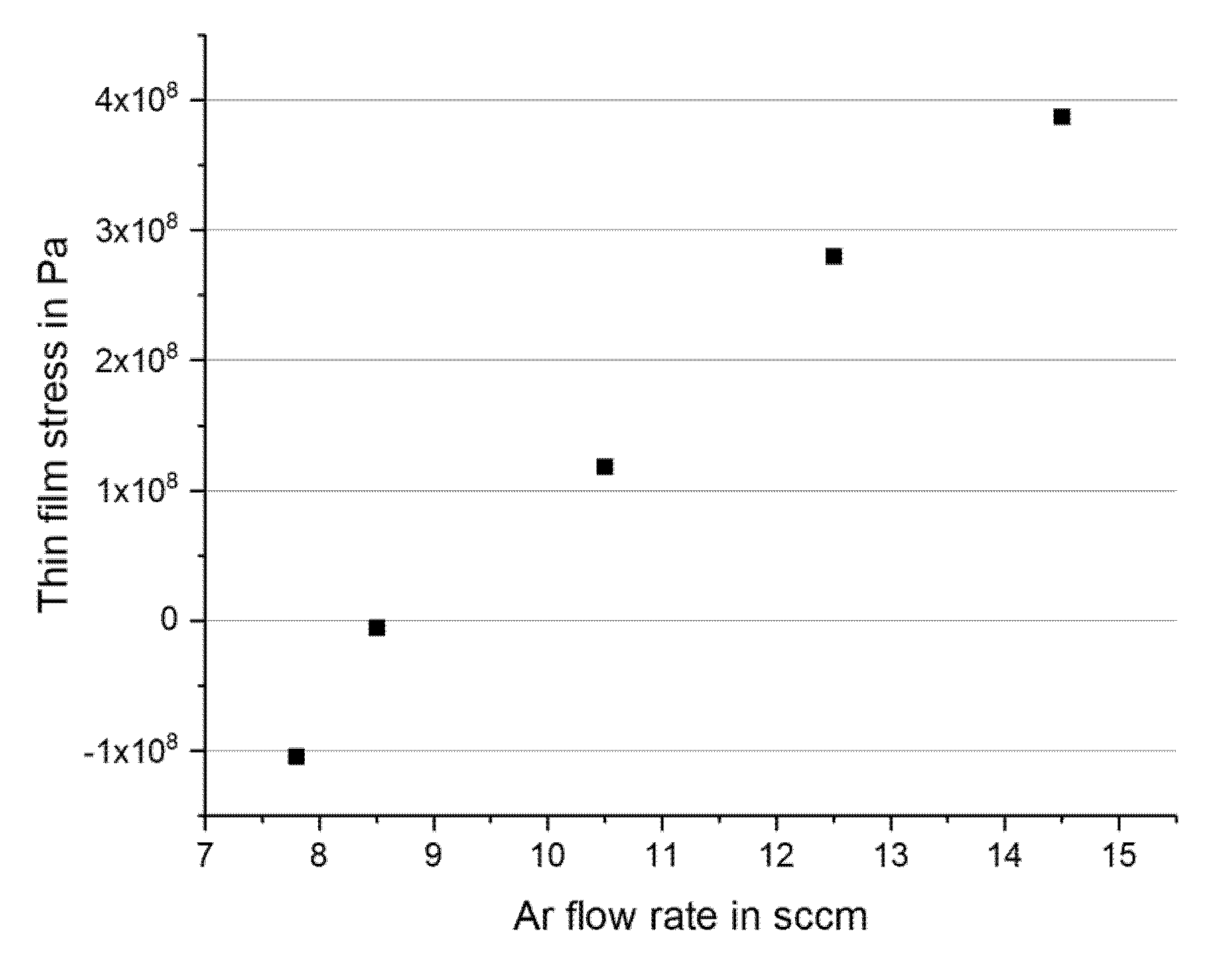
A 100-mm double-sided polished Si wafer (300 µm thick) was used as a substrate. The process began with the deposition of 1-µm-thick thermal SiO2. This layer worked as an electrical insulator and a mask for silicon backside etching. A functional layer of FeSiB was formed with a thickness of 1 µm after a Ti adhesion layer with a 20-nm thickness had been deposited by sputtering. Instead of sputtering from an alloy target, the equipment allowed for the simultaneous sputtering from the four targets used (ULVAC, QAM-4-S). By choosing the power of each target’s magnetron, the composition of the sputtered film could be precisely controlled. After measuring the sputter rate of each target, the sputter power was individually adjusted. The composition was confirmed by inductively coupled plasma mass spectrometry (ICP–MS). To achieve the desired composition of Fe79Si7B14, three targets—Fe, FeB (50:50 at%), and Si—were sputtered at 150, 75, and 150 W, respectively. The total deposition rate of the obtained film was 9.3 nm/min, and the ICP–MS measurement showed a composition of Fe78.88Si6.54B14.58. To reduce the intrinsic stress of the non-deflected diaphragm as much as possible, the sputter process was optimized. The stress of a sputtered thin film depends on many parameters, such as film thickness, substrate temperature, and sputter rate. In this case, the Ar flow rate was chosen as the optimization parameter, and all other conditions left unchanged.
The lowest stress was obtained as −5 MPa at an Ar flow rate of 8.5 sccm (
Figure 2). Below 7.8 sccm and above 15.5 sccm, no stable plasma could be maintained at the Fe target. The amorphous nature of the film was confirmed using X-ray diffraction (XRD D8 Advance, Bruker, Billerica, MA, USA). The metal film was etched by ion-beam milling. OFPR-800 200cp (Tokyo Ohka Kogyo, Tokyo, Japan) with a thickness of 3 µm was used as a photoresist mask. Next, Au electrodes were deposited. RF magnetron sputtering (CSF-4ES-232, Shibaura Mechatronics, Yokohama, Japan) was employed to deposit a 300-nm-thick blanket Au layer, with a 20-nm-thick Cr adhesion layer. Cr was used because it has good adhesion to both SiO
2 and FeSiB. Photolithography using OFPR-800 was again conducted on the blanket Au layer. The electrodes were then patterned by wet etching using aqueous iodine solution (KI + I
2). The photoresist was stripped after the etching process. Next, the SiO
2 on the backside was etched to form a mask for the Si reactive ion etching (RIE). Through the Bosch process (MUC-21, SPT, Tokyo, Japan), the diaphragm, which formed the core part of the pressure sensor, was opened from the backside. After that, the mask material on the backside and the isolation layer below the diaphragm, both of which were thermal SiO
2, were etched by RIE. During the etching, the front side was protected by photoresist. We observed no distortion of the membrane after completing the fabrication process. XRD analysis also showed that the amorphous nature of the FeSiB metal did not change as a result of the fabrication steps.
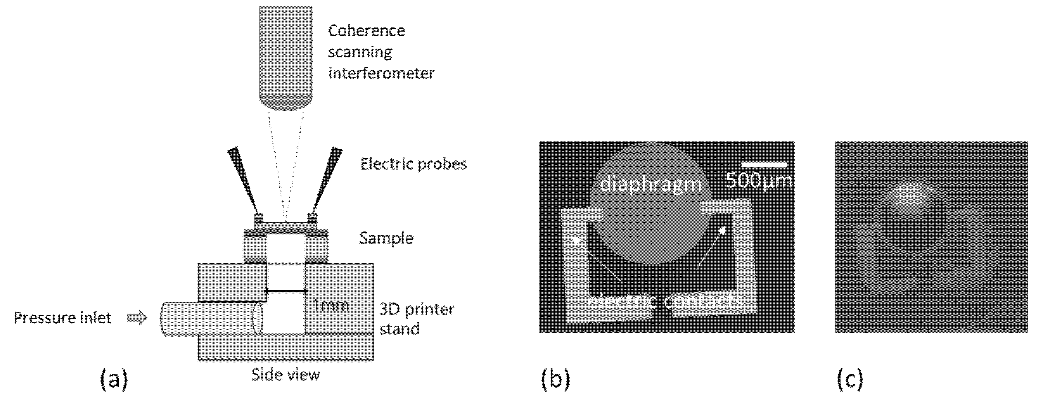
To characterize the diaphragm, the setup shown in
Figure 3 was prepared. It consisted of a 3D-printed stand where the demonstrator was mounted on top and an Ar gas source was connected via a tube. The pressure in the device was controlled by a PC via a microcontroller. The setup allowed for the observation of the device under test conditions from the top using a coherence scanning interferometer (Nexview, Zygo, Middlefield, CT, USA).
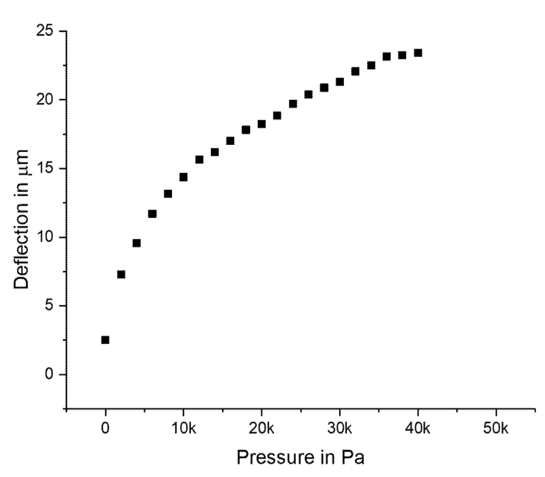
The deformation of the device was observed upon application of different pressures from the backside of the diaphragm—From 0 to 40 kPa in steps of 2000 Pa.
Figure 4 shows the deflection vs. pressure. It followed the expected nonlinear behavior for a fully clamped circular diaphragm with large deflection according to [
26]. The setup allowed for a maximum of 40 kPa to be applied. The diaphragm did not break in a test at maximum pressure.
The impedance of the device was measured by a network analyzer (E5071B, Agilent, Santa Clara, CA, USA) using a high-frequency (HF) probe station in the range from 5 to 500 MHz.
3. Results
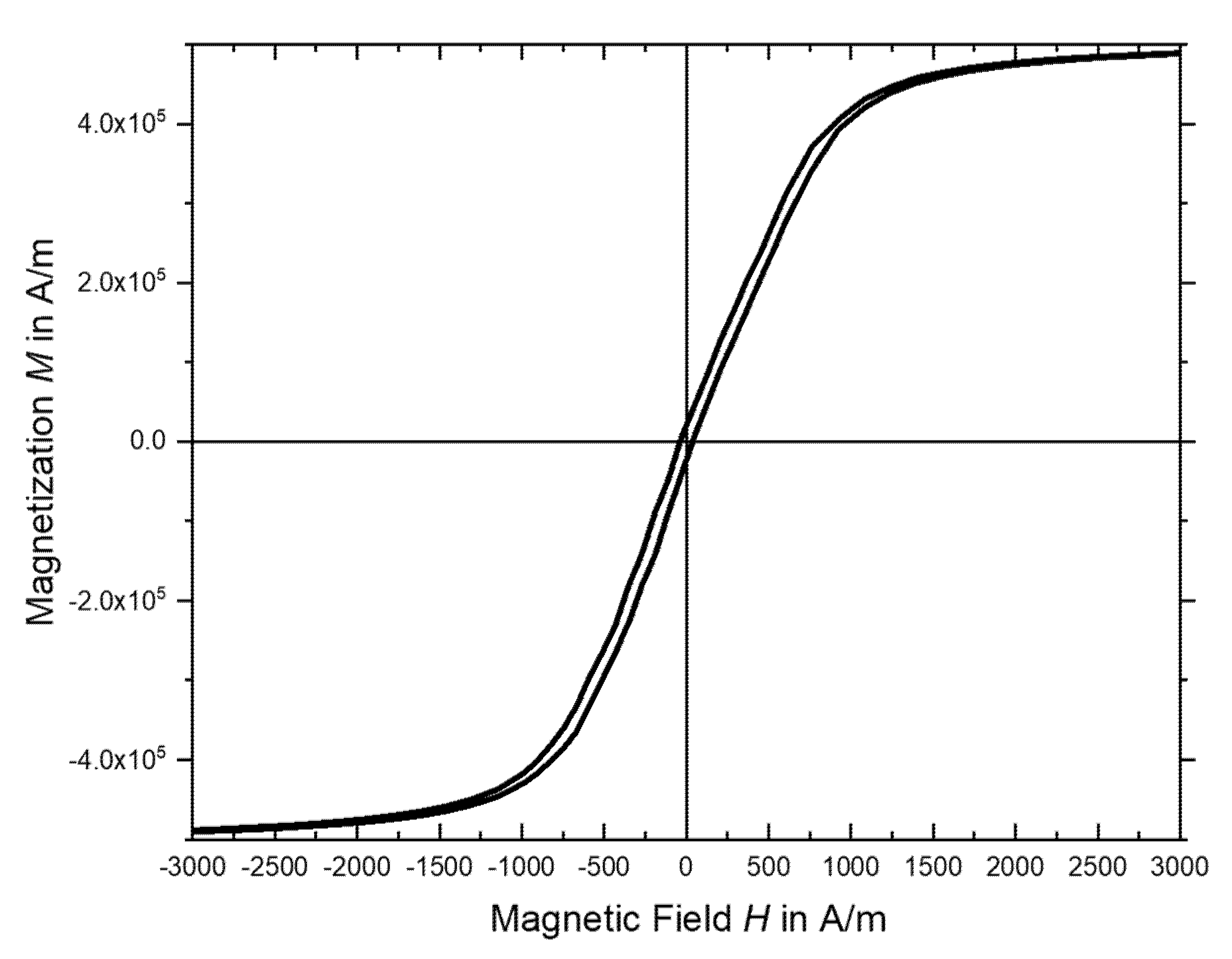
The basic electric and magnetic properties of the sputtered FeSiB film were measured. I-V characteristics were linear and the resistivity was determined by the 4-point probe method to be 1.65 µΩm. A superconducting quantum interference device (SQUID) was used to measure the in-plane direction magnetic hysteresis curve of the thin film at room temperature (
Figure 5). The parameters derived from the measurements are summarized in
Table 1.
The sputtered material clearly showed soft magnetic characteristics. The values were comparable with the films obtained by other groups [
2,
27].
A simple lumped equivalent circuit was used to model the electrical properties of the device. This model was useful to separate the effect of the parasitic elements of the device under test from the effect caused by stress that was induced in the diaphragm due to deformation by the pressure difference. The equivalent circuit consists of two serial branches, one of which consists of two parallel branches, as shown in
Figure 6.
The series branch of
L1 and
R1 represents the parasitic effect of the contact paths to the diaphragm.
C1 is caused by the capacitive feedthrough via the substrate, and
R2 represents the resistance of the substrate and non-moveable FeSiB. The soft magnetic transducer consists of
RSI and
LSI.
RSI is determined by considering the skin effect, and, in the case of a wide, very thin strip, it can be approximated as:
where
RDC is the
DC resistance and
t is the thickness of the film [
28]. The skin depth
δ is given by Equation (2).
LSI is caused by the self-inductance of the transducer material. In the case of a thin strip with a length
l and width
w >> thickness, it can be calculated as follows:
The impedance
ZSI is the impedance of the diaphragm metal:
Per Equations (2), (5), and (6) [
29], it can be seen that
RSI and
LSI, and therefore
ZSI, depend on the relative magnetic permeability
µr of the transducer metal.
To obtain the values of
R1,
R2,
L1, and
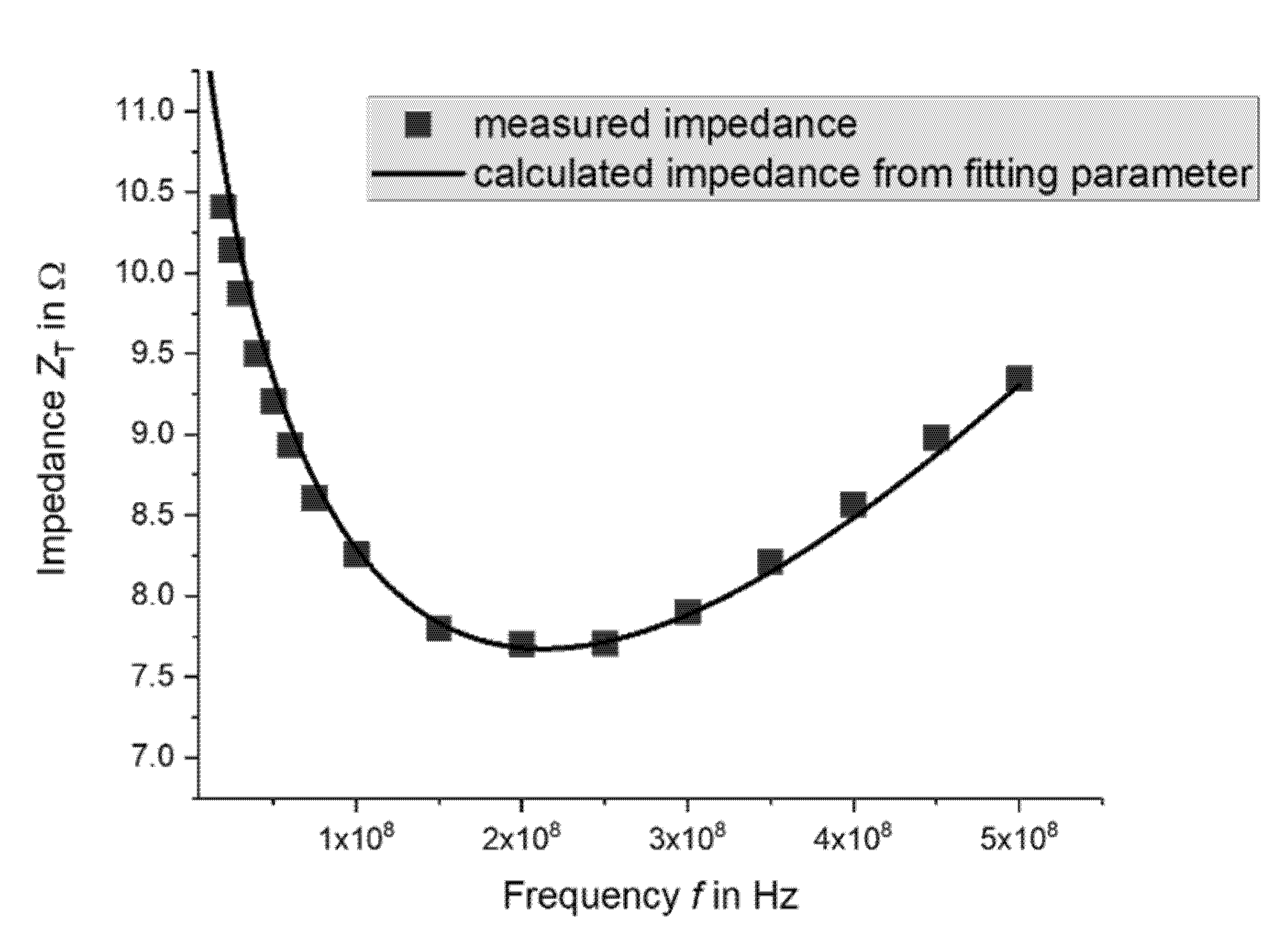
C1, the total impedance
ZT of the device was measured between 5 and 500 MHz, without inducing any deformation of the diaphragm using pressure. The total impedance
ZT of the device varied between 7.7 and 10.4 Ω, as shown in
Figure 7.
The values of the equivalent circuit elements were determined by fitting them with the target of minimizing the error Δ between the measured impedance
ZT and the calculated impedance
ZCalc, which is given as follows:
As the starting values of the fitting, the values estimated from the dimensions of the device were used. The Levenberg–Marquart method was employed as an algorithm to minimize Δ. The results with the best fitting are shown in
Table 2. The obtained values are reasonable for the parasitics of a device of this size. A comparison between the frequency characteristics of
ZT and the frequency characteristics obtained by calculation with the equivalent circuit shows a good agreement (
Figure 7).
The relative permeability µr of the soft magnetic film under this condition was also obtained as 2306 through fitting.
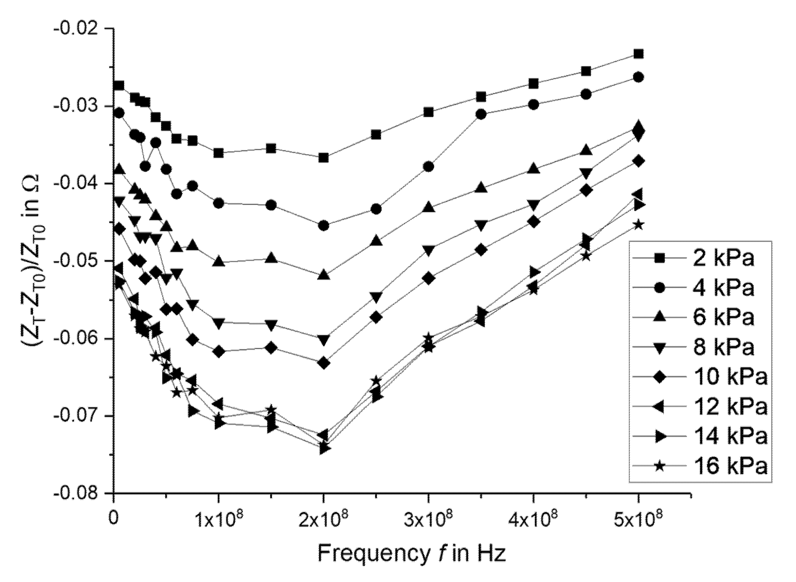
Figure 8 shows the change in the impedance of the device under different applied pressures. Over the entire frequency range, the impedance decreased with increasing pressure. The effect was the strongest at 200 MHz.
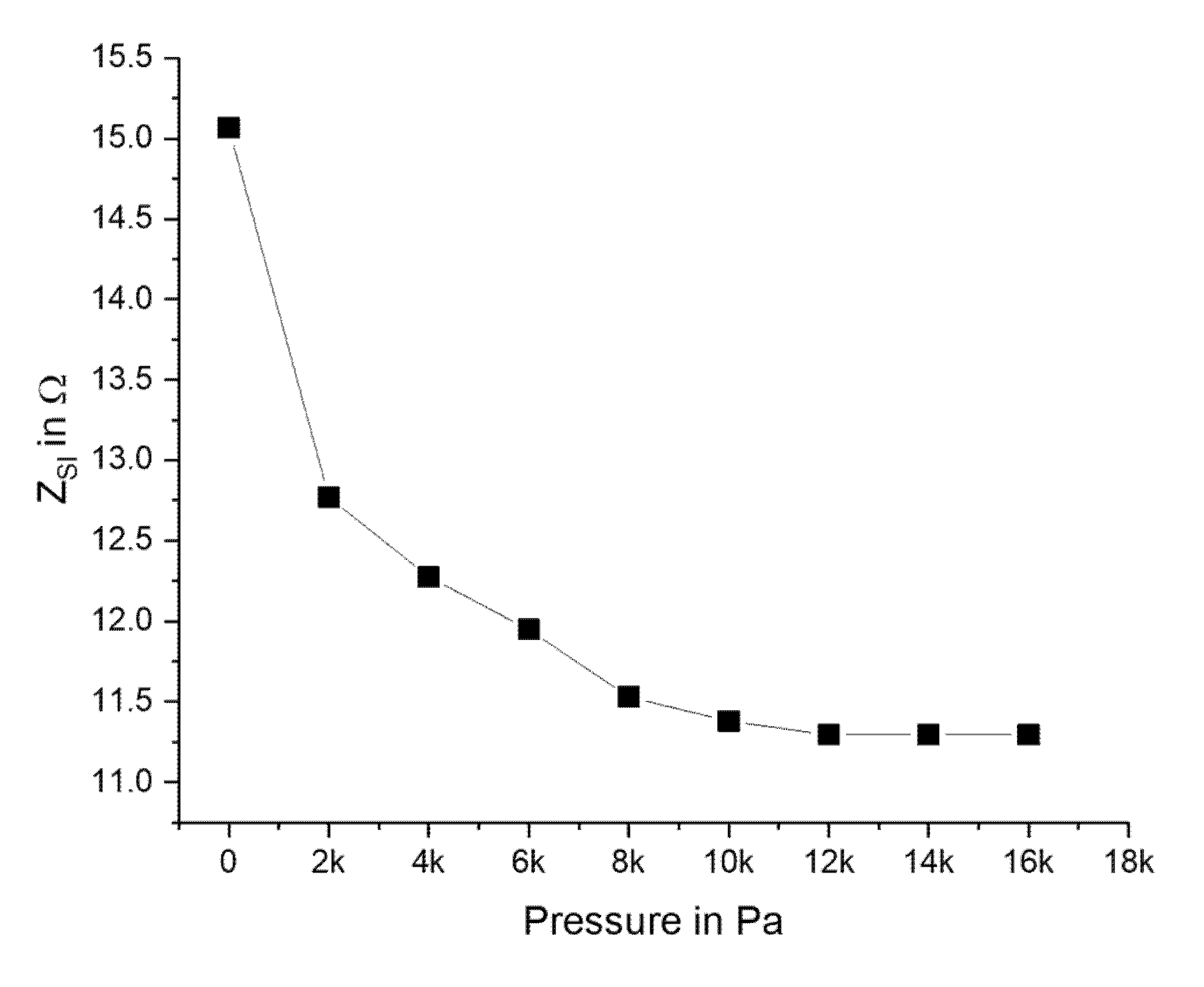
By applying the lumped element equivalent circuit, which was described earlier, it was possible to separate the impedance change of the diaphragm metallization (FeSiB)
ZSI from the total
ZT. The relation between
ZSI and the applied pressure is shown in
Figure 9. It decreased until 12 kPa, and after that, higher pressures did not lead to a further change in impedance.
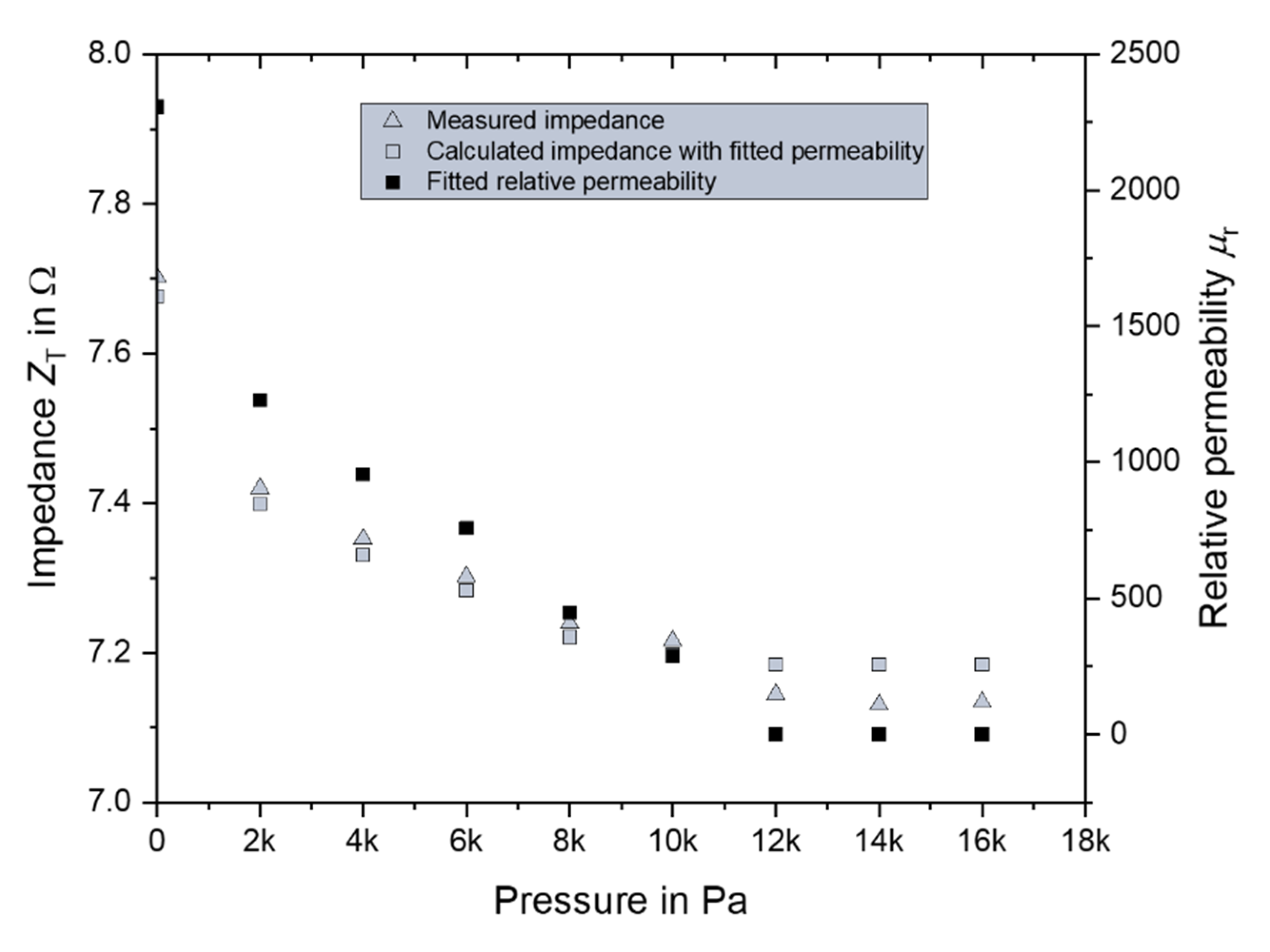
By using this result and Equations (5)–(7), the permeability of the FeSiB for each pressure step was obtained by fitting with the Levenberg–Marquart method, as shown in
Figure 10. The impedance was recalculated from the obtained permeability and was plotted on the same figure. It showed a good fitting with the measured impedance, indicating that the results were reasonable. At a pressure of 12 kPa, the relative permeability approached a value of 1, and the impedance did not vary greatly. The relationship between impedance and pressure was non-linear.
4. Discussion and Conclusions
The measurement results show a clear dependence of the impedance on the applied pressure. Additionally, it could be shown that the change in impedance can be observed by a change in the permeability of the soft magnetic FeSiB material. The applied pressure deforms the diaphragm and stress is created in the diaphragm. The stress causes a change in the magnetic anisotropy of the diaphragm material and, as a result, the permeability changes. The mechanical energy overcomes the domain wall energy and the domain wall moves. The measurement results show that, at a certain pressure, the impedance remains constant and the relative permeability approaches 1. We believe that this is because the magnetic material reached its saturation magnetization when its magnetic domain structure changed from multi domain to single domain under the induced stress. This is a limitation of the device.
To evaluate the usefulness of such a simple structure as a pressure sensor, we calculated the gauge factor
GF, as in Equation (4). For this, the strain must be obtained. As the diaphragm is much thinner than its radius, the stress is approximated as being constant over the entire diaphragm. If the bending moments are small, the deflection is a function of the intrinsic stress and the elastic straining of the membrane. If the radial strain
εr is assumed as being constant over the entire membrane, it can be estimated from the difference in the length of the diameter (2
r) of an undeflected membrane and the segment of a parabola, corresponding to the cross-section of a membrane with a center deflection of
w0, as follows:
The strongest change in impedance was observed at 200 MHz. It is close to the electric resonance of the device where the reactance is at its minimum, reducing the influence of the parasitic elements. At 12 kPa pressure, the center deflection of the diaphragm
w0 was 15.6 µm, and the transducer impedance
ZSI was 11.29 Ω. In the initial state (0 Pa), the impedance of the transducer was 15.07 Ω. By using Equations (4) and (9) [
30], the result of
GF = 385.7 could be obtained. The gauge factor was much higher than that of metal strain gauges (<10) and slightly higher than that of silicon strain gauges (~200). Although it was much lower than the optimized SI effect strain gauges, this very simple pressure sensor still demonstrates good potential for application. The sensitivity of the device is determined by the mechanical compliance of the diaphragm and the relationship between induced stress and impedance change. Mechanical compliance of a fully clamped circle diaphragm is defined as:
where
E is the Young’s modulus,
ϑ is the Poisson’s ratio, and
P is the applied pressure. It can be seen that a thinner and larger diaphragm results in larger deflection at the same pressure. As a result, the strain and stress in the diaphragm are larger and the gauge factor should be higher. On the other hand, as shown in Equation (5), the impedance change of the diaphragm will be larger with higher
t at the same
∆δ, and if
t <<
δ, the impedance change will be too small. Additionally,
t and
r of the diaphragm are also important for the maximum sustainable pressure. A diaphragm design should be optimized based on the sensor requirements.
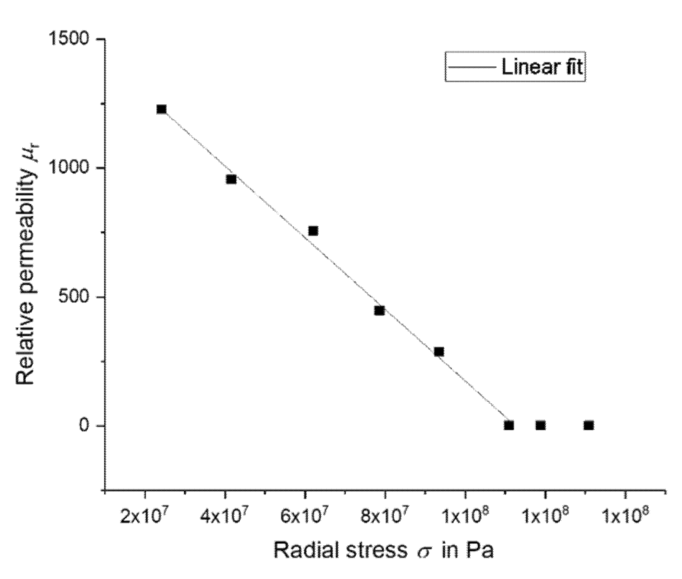
Under the assumption of Young’s modulus
E = 170 GPa [
31] and the strain obtained by Equation (9), it is possible to calculate the radial stress
σ and to plot it against the relative permeability.
Figure 11 shows this relationship.
Up to a relative permeability value approaching 1, it appeared to have a linear relation with the radial stress in the diaphragm. To confirm this relation,
µr should be obtained directly by measurement in a vibrating-sample magnetometer (VSM) under different applied stresses in future experiments. In the related theory, it is known that magnetic permeability depends on the magnetic field acting on it [
32]. However, a complete quantitative model of permeability as a function of mechanical stress has not yet been published. An advanced solution was proposed in reference [
13]. The effective magnetic field in the material
Heff also considers the influence of mechanical stresses as linear:
H is the applied magnetic field,
M is the magnetization of the material, and
α is a dimensionless parameter representing interdomain coupling. The saturation magnetostriction
λS may also depend on stress [
33].
The impedance change of the diaphragm vs. the pressure change ( ) was nonlinear, with a larger change at lower pressures. The reason is the also nonlinear mechanical behavior of the diaphragm at large deflections, as well as the complex relationship between µ and ZSI, as shown in Equations (2) and (5)–(7).
In this investigation, at a relative pressure of 40 kPa, a maximum stress of 250 MPa was applied to the diaphragm. It did not break or show any kind of damage. To obtain information about the structural stability of the diaphragm, its XRD pattern was recorded just after sputtering, after device fabrication, and after 10 times of applying of the maximum pressure to the device.
Figure 12 shows the results. Beside the peaks resulting from the silicon substrate, Ti from the adhesion layer was detected after sputtering. There were no other sharp peaks detected, confirming that the FeSiB was in an amorphous state. After device fabrication and after applying the maximum possible pressure of 40 kPa, no apparent change in the diffraction pattern was observed. The impedance of the device also did not change. It can be concluded that the amorphous structure did not change during fabrication or under load.
It is known that amorphous FeSiB can have an extremely high tensile strength of more than 3.5 GPa [
34]. This can sustain much larger strains than conventional strain transducers or fabricate very thin diaphragms with high mechanical compliance. Additionally, the transducer is just a simple diaphragm without structure or additional layers and can be fabricated easily. Typical micro machined pressure sensors using piezoresistive strain gauges, integrated into a silicon diaphragm. Beside the processes to fabricate the diaphragm itself, silicon piezoresistive strain gauges require several process steps, such as ion implantation and thermal diffusion, to create different doped regions in the semiconductor material of the diaphragm. By contrast, our proposed device only needs magnetron sputtering to form the diaphragm, as the diaphragm itself is already the transducer. Several lithography mask layers (to form the piezoresistive transducers in the diaphragm) are not needed. Furthermore, FeSiB, the material for the diaphragm, is not expensive and used for thin-film magnetic field sensors [
2,
7]. We believe that the proposed simple device has a good potential for use as a cheap sensor, with
GF being at least as good as piezoresistive sensors. The influence of external electro-magnetic fields and other noise sources should be investigated in future work. To increase the magnetic anisotropy, permeability, and ultimately the
GF, thermal annealing of the transducer metal, preferably in an external magnetic field, should be carried out in an attempt to improve the performance [
35]. Another method is to apply a constant magnetic field during the deposition process.


