Thin-Film MEMS Resistors with Enhanced Lifetime for Thermal Inkjet

Abstract
1. Introduction
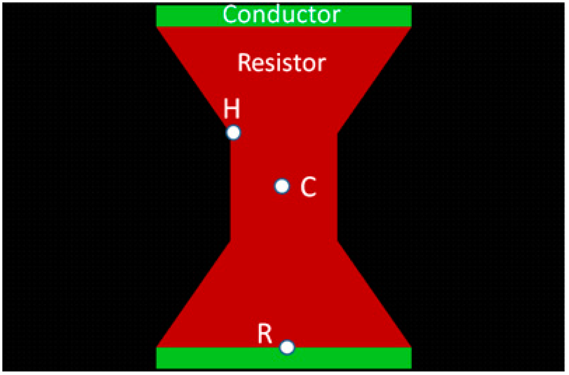
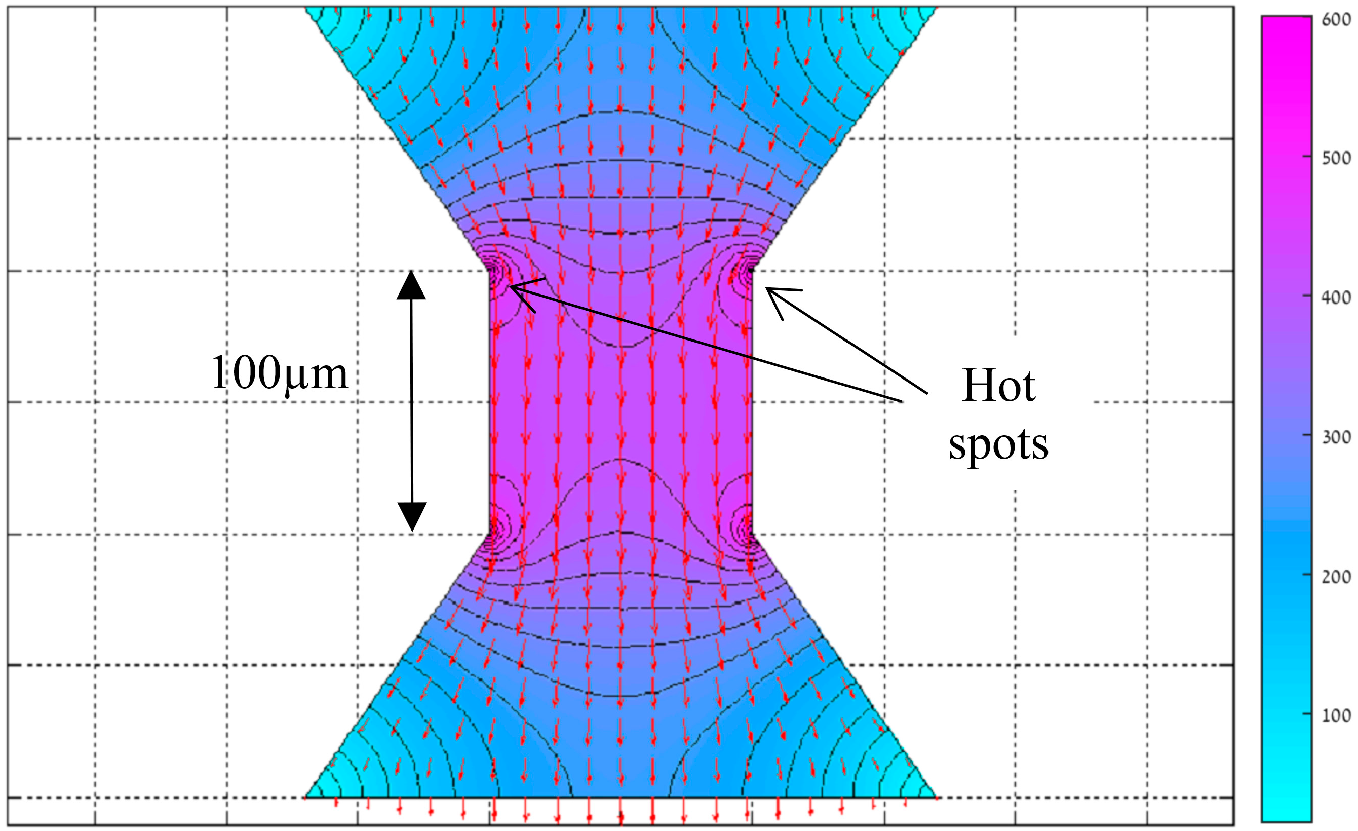
2. Thermal Gradients in Resistors
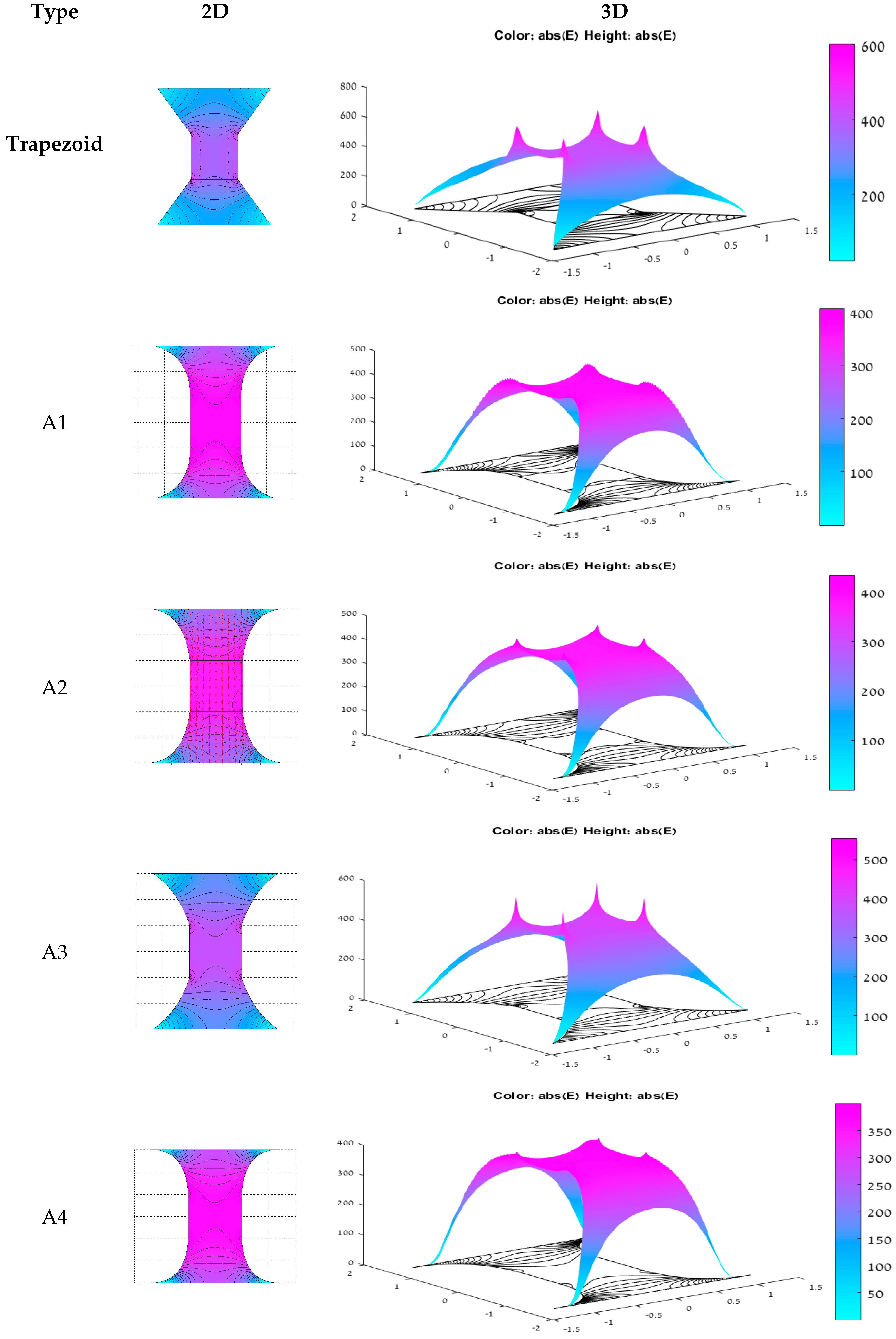
3. Resistors Simulation
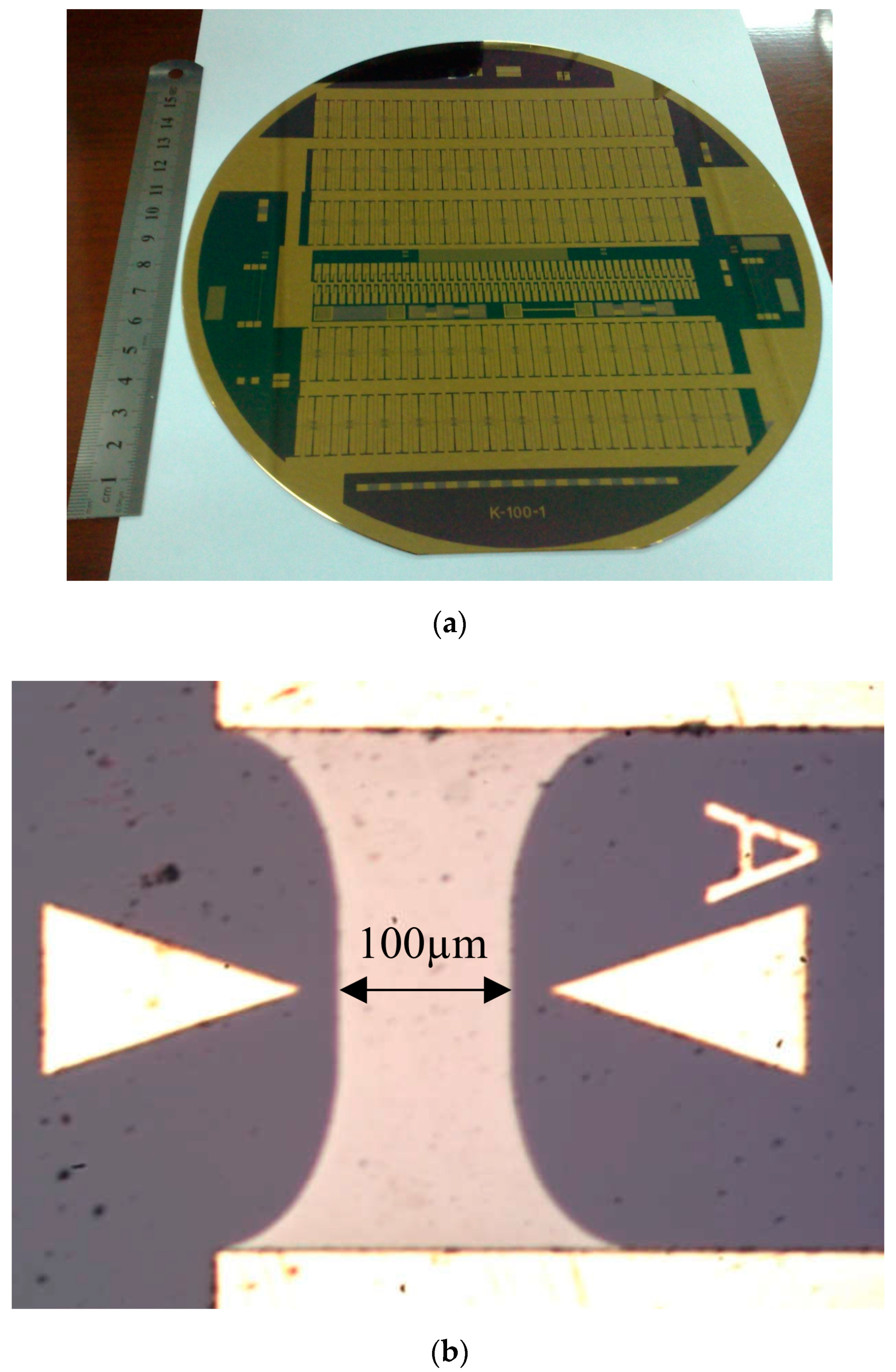
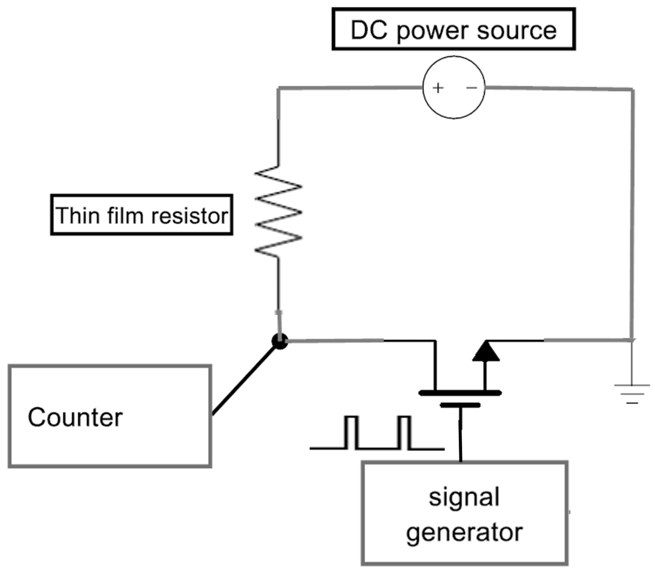
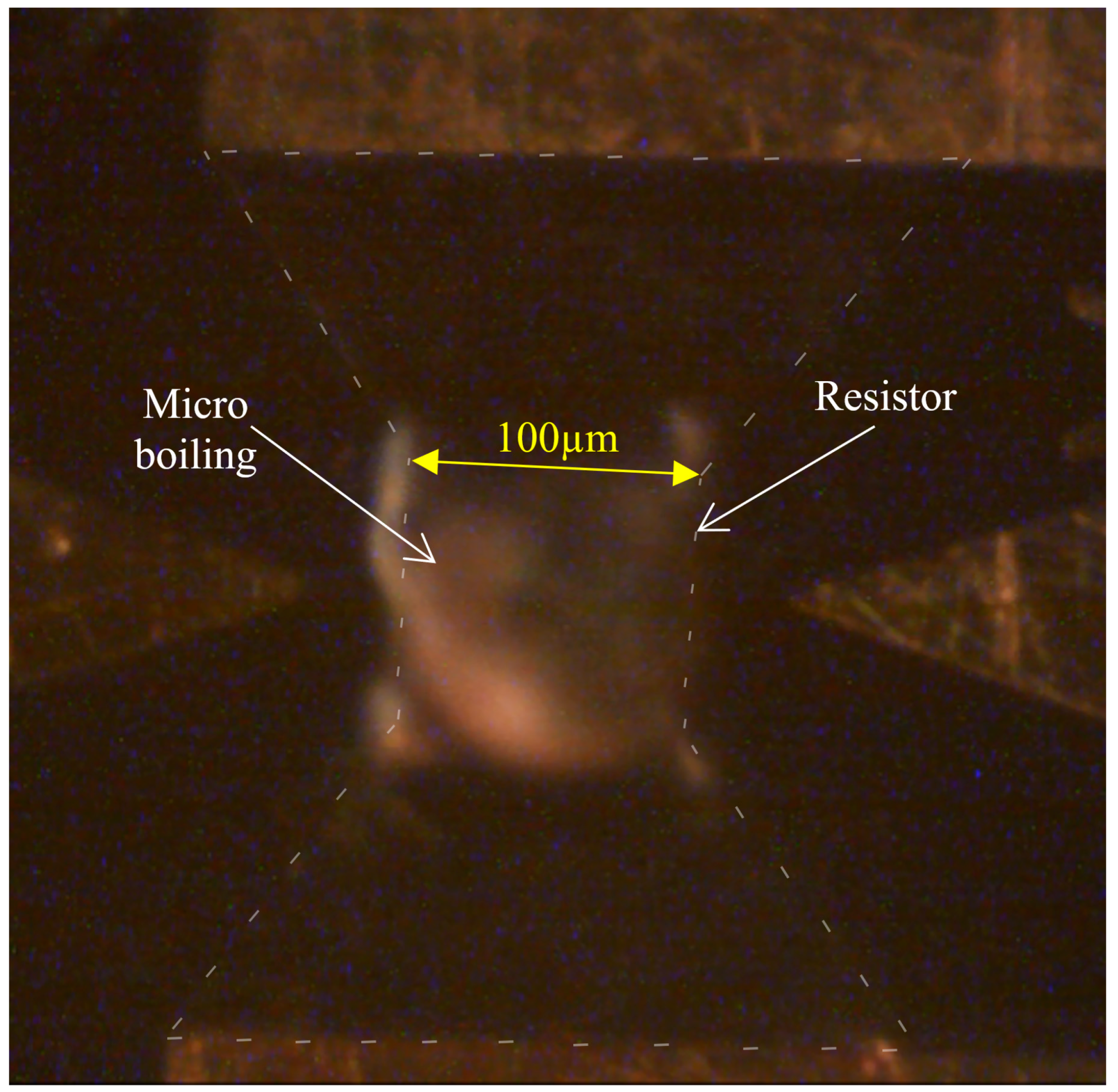
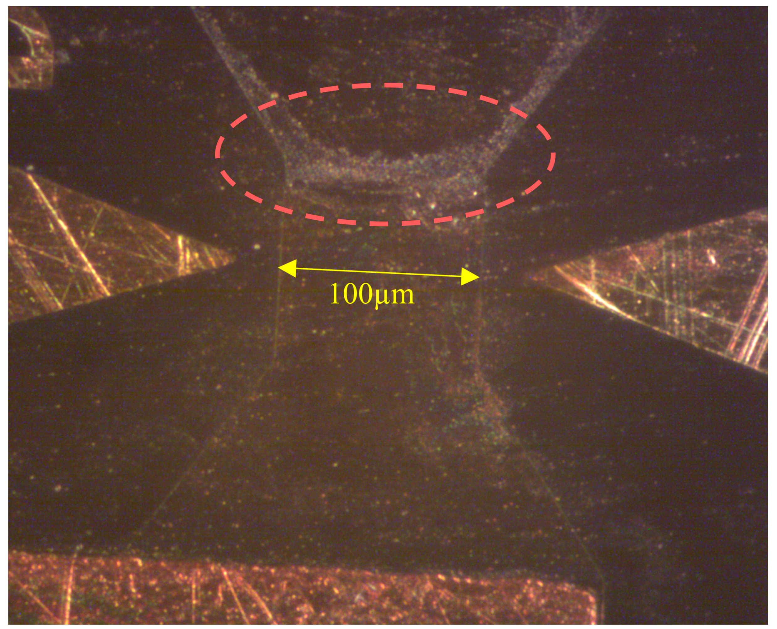
4. Experiment and Results
5. Discussion and Conclusions
Author Contributions
Funding
Conflicts of Interest
References
- Hoath, S.D. (Ed.) Fundamentals of Inkjet Printing: The Science of Inkjet and Droplets; Wiley-VCH Verlag GmbH & Co. KGaA: Weinheim, Germany, 2016. [Google Scholar]
- Zapka, W. (Ed.) Handbook of Industrial Inkjet Printing: A Full System Approach; Wiley-VCH Verlag GmbH & Co. KGaA: Weinheim, Germany, 2018. [Google Scholar]
- Hutchings, I.M.; Martin, G.D. (Eds.) Inkjet Technology for Digital Fabrication; John Wiley & Sons, Ltd.: Chichester, UK, 2013. [Google Scholar]
- Le, H.P. Progress and trends in ink-jet printing technology. J. Imaging Sci. Technol. 1998, 42, 49–62. [Google Scholar]
- Hoefemann, H.; Wadle, S.; Bakhtina, N.; Kondrashov, V.; Wangler, N.; Zengerle, R. Sorting and lysis of single cells by BubbleJet technology. Sens. Actuators B Chem. 2012, 168, 442–445. [Google Scholar] [CrossRef]
- De Wijs, K.; Liu, C.; Dusa, A.; Vercruysse, D.; Majeed, B.; Tezcan, D.S.; Blaszkiewicz, K.; Loo, J.; Lagae, L. Micro vapor bubble jet flow for safe and high-rate fluorescence-activated cell sorting. Lab Chip 2017, 17, 1287–1296. [Google Scholar] [CrossRef] [PubMed]
- Majeed, B.; Liu, C.; Van Acker, L.; Daily, R.; Miyazaki, T.; Sabuncuoglu, D.; Lagae, L.; Miyazaki, T. Fabrication of silicon-based microfluidics device for cell sorting application. In Proceedings of the 2014 IEEE 64th Electronic Components and Technology Conference (ECTC), Orlando, FL, USA, 27–30 May 2014; pp. 165–169. [Google Scholar]
- Scoutaris, N.; Ross, S.; Douroumis, D. Current Trends on Medical and Pharmaceutical Applications of Inkjet Printing Technology. Pharm. Res. 2016, 33, 1799–1816. [Google Scholar] [CrossRef] [PubMed]
- Tan, H. Numerical study of a bubble driven micromixer based on thermal inkjet technology. Phys. Fluids 2019, 31, 062006. [Google Scholar] [CrossRef]
- Liou, J.-C.; Wu, C.-C. Design and fabrication of microfluidic inkjet chip with high voltage ESD protection system for DNA droplets arrangement and detection. Microsyst. Technol. 2015, 23, 199–213. [Google Scholar] [CrossRef]
- Mattana, G.; Loi, A.; Woytasik, M.; Barbaro, M.; Noël, V.; Piro, B. Inkjet-Printing: A New Fabrication Technology for Organic Transistors. Adv. Mater. Technol. 2017, 2, 1700063. [Google Scholar] [CrossRef]
- Khan, A.; Rahman, K.; Hyun, M.-T.; Kim, N.-S.; Choi, K.-H. Multi-nozzle electrohydrodynamic inkjet printing of silver colloidal solution for the fabrication of electrically functional microstructures. Appl. Phys. A 2011, 104, 1113–1120. [Google Scholar] [CrossRef]
- Huang, C.; Tsou, C. The implementation of a thermal bubble actuated microfluidic chip with microvalve, micropump and micromixer. Sens. Actuators A Phys. 2014, 210, 147–156. [Google Scholar] [CrossRef]
- Sourtiji, E.; Peles, Y. A micro-synthetic jet in a microchannel using bubble growth and collapse. Appl. Therm. Eng. 2019, 160, 114084. [Google Scholar] [CrossRef]
- Law, J.; Kong, K.W.; Chan, C.; Sun, W.; Li, W.J.; Chau, E.B.F.; Chan, G.K.M. Atomization of High-Viscosity Fluids for Aromatherapy Using Micro-heaters for Heterogeneous Bubble Nucleation. Sci. Rep. 2017, 7, 40289. [Google Scholar] [CrossRef] [PubMed]
- Bonfert, D.; Gieser, H.; Bock, K.; Svasta, P.; Ionescu, C. Electrical stress on thin film TaN resistive structures. In Proceedings of the IEEE 17th International Symposium for Design and Technology in Electronic Packaging (SIITME), Timisoara, Romania, 20–23 October 2011; pp. 313–318. [Google Scholar]
- Khalate, A.; Bombois, X.; Scorletti, G.; Babuska, R.; Koekebakker, S.; De Zeeuw, W. A Waveform Design Method for a Piezo Inkjet Printhead Based on Robust Feedforward Control. J. Microelectromech. Syst. 2012, 21, 1365–1374. [Google Scholar] [CrossRef]
- Singh, M.; Haverinen, H.M.; Dhagat, P.; Jabbour, G.E. Inkjet Printing-Process and Its Applications. Adv. Mater. 2010, 22, 673–685. [Google Scholar] [CrossRef] [PubMed]
- Khalate, A.; Bomboisa, X.; Babuškaa, R.; Wijshoffb, H.; Waarsingb, R. Performance improvement of a drop-on-demand inkjet printhead using an optimization-based feed forward control method. Control Eng. Pract. 2011, 19, 771–781. [Google Scholar] [CrossRef]
- Baca, A.G.; Overberg, M.E.; Wolfley, S.L.; Fortune, T.R. A thin film TaN resistor reliability evaluation. In Proceedings of the 2017 IEEE International Reliability Physics Symposium (IRPS), Monterey, CA, USA, 2–6 April 2017. [Google Scholar] [CrossRef]
- Lee, T.; Watson, K.; Chen, F.; Gill, J.; Harmon, D.; Sullivan, T.; Li, B. Characterization and reliability of TaN thin film resistors. In Proceedings of the 2004 IEEE International Reliability Physics Symposium, Phoenix, AZ, USA, 25–29 April 2004; pp. 502–508. [Google Scholar] [CrossRef]
- Dąbrowski, A.; Dziedzic, A. Stability of low ohmic thick-film resistors under pulsed operation. Microelectron. Reliab. 2018, 84, 95–104. [Google Scholar] [CrossRef]
- Liou, J.; Yang, C.; Gong, C. Design and Fabrication of Identification Inkjet Print Head Chip Fuse Sensors. Sens. Mater. 2016, 28, 493–501. [Google Scholar]
- Park, J.-H.; Oh, Y. Investigation to minimize heater burnout in thermal thin film print heads. Microsyst. Technol. 2005, 11, 16–22. [Google Scholar] [CrossRef]
- Lim, J.-H.; Kuk, K.-; Shin, S.-L.; Baek, S.-S.; Kim, Y.-L.; Oh, Y.-S. Investigation of reliability problems in thermal inkjet printhead. In Proceedings of the 2004 IEEE International Reliability Physics Symposium, Phoenix, AZ, USA, 25–29 April 2004; pp. 251–254. [Google Scholar]
- McGlone, J.M.; Pommerenck, J.; Graham, M.W.; Wager, J.F. Amorphous Metal Thin Films for Thermal Inkjet Printing. J. Microelectromech. Syst. 2018, 27, 289–295. [Google Scholar] [CrossRef]
- Liu, B.; Hou, Y.P.; Desheng, L.I.; Yang, J.H. A thermal bubble micro-actuator with induction heating. Sens. Actuators A Phys. 2015, 222, 8–14. [Google Scholar] [CrossRef]
- Einat, M.; Grajower, M. Microboiling Measurements of Thermal-Inkjet Heaters. J. Microelectromech. Syst. 2010, 19, 391–395. [Google Scholar] [CrossRef]
- Einat, M.; Einat, N. Two-dimension full array high-speed ink-jet print head. Appl. Phys. Lett. 2006, 89, 73505. [Google Scholar] [CrossRef]
- Einat, M.; Bar-Levav, E. 2D segmented large inkjet printhead for high speed 3D printers. J. Micromech. Microeng. 2015, 25, 5. [Google Scholar] [CrossRef]


| Shape | E(C) (v/m) | E(H) (v/m) | E(R) (v/m) | En(H) | En(R) |
|---|---|---|---|---|---|
| A1 | 371.3 | 397 | 274.2 | 107% | 74% |
| A2 | 377.3 | 443.3 | 273.2 | 117% | 72% |
| A3 | 397.9 | 587.3 | 256.6 | 148% | 64% |
| A4 | 368.4 | 404.7 | 278 | 110% | 75% |
| Trapezoid | 415.2 | 588.7 | 247.1 | 142% | 60% |
| Resistor Shape | En(R) | En(H) | Average Number of Pulses until Breakdown |
|---|---|---|---|
| Trapezoid | 60% | 142% | 2.02 × 10 8 |
| A3 | 64% | 148% | 2.75 × 10 8 |
| A2 | 72% | 117% | 1.88 × 10 9 |
| A4 | 75% | 110% | 2.35 × 10 9 |
| A1 | 74% | 107% | 2.49 × 10 9 |
© 2020 by the authors. Licensee MDPI, Basel, Switzerland. This article is an open access article distributed under the terms and conditions of the Creative Commons Attribution (CC BY) license (http://creativecommons.org/licenses/by/4.0/).
Share and Cite
Bar-Levav, E.; Witman, M.; Einat, M. Thin-Film MEMS Resistors with Enhanced Lifetime for Thermal Inkjet. Micromachines 2020, 11, 499. https://doi.org/10.3390/mi11050499
Bar-Levav E, Witman M, Einat M. Thin-Film MEMS Resistors with Enhanced Lifetime for Thermal Inkjet. Micromachines. 2020; 11(5):499. https://doi.org/10.3390/mi11050499
Chicago/Turabian StyleBar-Levav, Elkana, Moshe Witman, and Moshe Einat. 2020. "Thin-Film MEMS Resistors with Enhanced Lifetime for Thermal Inkjet" Micromachines 11, no. 5: 499. https://doi.org/10.3390/mi11050499
APA StyleBar-Levav, E., Witman, M., & Einat, M. (2020). Thin-Film MEMS Resistors with Enhanced Lifetime for Thermal Inkjet. Micromachines, 11(5), 499. https://doi.org/10.3390/mi11050499