Abstract
This review collates around 100 papers that developed micro-electro-mechanical system (MEMS) capacitive microphones. As far as we know, this is the first comprehensive archive from academia on this versatile device from 1989 to 2019. These works are tabulated in term of intended application, fabrication method, material, dimension, and performances. This is followed by discussions on diaphragm, backplate and chamber, and performance parameters. This review is beneficial for those who are interested with the evolutions of this acoustic sensor.
1. Introduction
Ever since the introduction of modern microphone back in the late 19th century, tremendous progress had been made due to its broad and evolving list of applications in consumer [1,2], medical [3,4], and automotive applications [5,6]. Johann Philipp Reis and Alexander Graham Bell are acknowledged as the inventors of the first microphones [7]. These early prototypes produced electrical signals with low amplitude and limited frequency ranges. As a result, the sound quality was so low that the devices were barely capable of reproducing intelligible speech. The development of the functioning microphones was credited to Thomas Edison, Emile Berliner, and David Edward Hughes [8]. Their carbon microphones later dominated the markets. Edison and Berliner separately announced their inventions (called transmitters back then) and fought over the patent right in the United States. In the United Kingdom, Hughes demonstrated similar device to the Royal Society in London and coined the term microphone, although he did not apply for a patent. The telecommunications industry quickly realized the potential of microphones in their systems and pushed for technological innovations. The variants of the carbon microphone were commonly used in telephone between 1920s and 1980s. Riding on the rapid growth of telecommunication and music industries, other forms of transduction mechanisms continue to be developed and employed in the telecommunication systems. A capacitive microphone was introduced in 1916 and currently dominates the markets. The newest kinds are the optical-based and spintronic microphones.
There are a variety of transduction mechanisms being used in microphones to convert acoustic waves to electrical signal, such as electromagnetic (electrodynamic), piezoresistive, piezoelectric, optical, spintronic, and capacitive. For the first mechanism, an electromagnetic microphone consists of a coil that moves through a fixed magnetic field to produce the alternate current, i.e., electrical output. The coil is attached to a thin diaphragm that vibrates according to the acoustical input. The carbon- and ribbon microphones are the variants of this type [9,10,11]. An electromagnetic microphone has a sensitivity issue due to the slow vibrating velocity of heavy diaphragm and coil [12]. The second mechanism is called piezoresistive microphone. It operates as follows. On top of an acoustic diaphragm, there are four resistors that are connected in a Wheatstone bridge. When the pressure is induced by the sound waves, the diaphragm deflects. Accordingly, the stress-dependent values of the four resistors changes, as well. The Wheatstone bridge produces an output voltage based on the difference between the values of these resistors. Piezoresistive microphone has the disadvantages of relatively low dynamic range and sensitivity [13] but is nevertheless being used in many applications. The third mechanism is called piezoelectric microphone. It uses the principle of piezoelectricity to convert mechanical vibrations from sound waves to electrical signals [14]. For this purpose, aluminum nitride and zinc oxide are the common piezoelectric materials that researchers used to fabricate the thin diaphragm. Due to the rigidity of this material, this type of microphone is originally used to amplify contact-based vibration from musical instruments. Due to its advanced performances today, it has more diverse applications. As for the fourth mechanism, an optical or fiber-optic microphone uses light source to illuminate the thin diaphragm. A photo detector is used to detect the light’s intensity and wavelength. When the diaphragm is vibrated by the acoustic waves, the difference between the original and the reflected sources is recorded and further converted to electrical signal. Optical microphone’s main strength is that it is not susceptible to electrical noise and electromagnetic interference. The disadvantage is the complexity of the detection system, which translate to higher cost. It has niche markets in medical applications and high-fidelity recordings. Spintronic microphone is the fifth mechanism, which is based on magneto-resistance transduction. It is proposed to solve the low sensitivity issue that haunts piezoresistive microphone. The spin strain gauge sensor (SGS) replaces resistors on top of the acoustic diaphragm. This spin SGS is highly sensitive as it is based on magnetic tunnel junction effect. This approach was recently proposed by the Japanese researchers [15,16,17,18]. The sixth mechanism is called condenser microphone or more commonly known as capacitive microphone. It functions via changes in capacitance between movable and fixed plates. The thin diaphragm represents the movable plate. Incoming sound waves vibrate it, thus proportionally varying the value of the capacitance. A voltage source is needed to bias the plates at a fix voltage. The electret microphone is a specific type of capacitive microphone that keeps a permanent bias between its plates by means of an electret material. Due to its good performance, low cost, and ease of manufacture, the electret microphone became the most commercially manufactured microphone type with over one billion units produced annually at the height of its production [19].
A micro-electro-mechanical system (MEMS) microphone, which is the micro-scale version of the microphone, gained its footing in the commercial mobile market in the early 2000s, mostly due to the cost and footprint. Since its inception into mobile devices, the market began to skyrocket. The main driver for its rapid growth is because major phone manufacturers are putting as many as eight MEMS microphones into a single mobile device. In addition to acoustical-to- electrical signal conversion, this device is very versatile and could be used to replace other expensive sensors. For example, an array of MEMS microphones can be programmed to map an acoustical image [20,21] and moving vehicle [22]. Another future application is as proximity sensor, by setting the MEMS microphone to operate in the ultrasonic range. It can sense finger movements hovering a few millimeters above the mobile phone’s touchscreen to avoid physical contact. As a result, the phone’s screen will not get dirty and greasy [23].
In addition to mobile phones, electronics manufacturers are integrating MEMS microphones and other sensors into various handheld devices, smart watches, tablets, medical devices, wearable electronics, and Internet of Things (IoT) devices. Jérémie Bouchaud and Marwan Boustany of IHS Markit analyzed consumer and mobile MEMS markets from 2010 to 2018 [24]. They highlighted three important trends. First, the growth of MEMS market has expanded from slightly below $2 billion USD in 2010 to over 5 billion USD in 2017. Second, the top three products that employ MEMS sensors are mobile handsets, media tablets and wearable electronics. Third, all these devices heavily employ MEMS microphones. This market push solidifies the importance of MEMS microphone for years to come.
One of the earlier adopters of MEMS microphone is Apple, Inc. This company has been rigorously incorporating MEMS capacitive microphones into their iPhone products since the development of the iPhone 4 [25]. Knowles Technology and Infineon Technologies won the design for the three MEMS microphones incorporated in the iPhone 4, two for primary audio sensing and one for background pickup for noise cancelation. Knowles’ S4.10 and S2.14 microphones have a circular top movable diaphragm diameter of approximately 0.5 mm. The size is sufficient to capture sound wavelength, which is approximately 34 mm at 10 kHz. Both have die area of less than 1.6 mm2, with either two or four leads for interconnections. Knowles microphones utilize damping holes that co-functions as etch release vents during the fabrication process. Besides Knowles, Infineon Technologies provided the E2002 MEMS microphone for the iPhone 4. It has circular diaphragm with the diameter of 1 mm. Since the iPhone 4, capacitive microphones from Knowles and Infineon, along with microphones from other key manufacturers, such as Analog Devices, have won design contracts for various subsequent Apple products, including later generation iPhones and the iPod Nano. For example, Analog Devices designed the ADMP 403 MEMS microphone for the 5th generation iPod Nano. They proposed a circular diaphragm with a diameter of 0.59 mm.
The basic structure of MEMS capacitive microphone is shown in Figure 1. It consists of two parallel plates, i.e., movable top diaphragm and fixed backplate. Both are separated by an air gap, and an insulator was used as the spacer. The top and bottom plates are connected to separate electrodes that measure the output signal. The diaphragm vibrates when acoustic pressure is applied onto it, hence producing variation in the air gap. The resulting parallel plate capacitance is given by Equation (1):
where , A, and g is capacitance, permittivity of the dielectric material, area of the plate, and air gap, respectively. The value of the measured capacitance is proportional and inversely proportional to the size of the diaphragm and air gap, respectively.
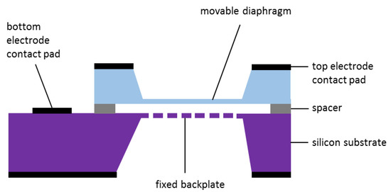
Figure 1.
Basic structure of a micro-electro-mechanical system (MEMS) capacitive microphone.
The perforated backplate is shown as a dashed line in Figure 1, of which the dashes represent acoustic holes. They enable air to stream in and out of the air gap when the diaphragm vibrates. Without these holes, the squeezed air between the diaphragm and backplate becomes a mechanical dampener. It reduces the ability of the diaphragm to vibrate, especially at higher frequency. In other words, the sensitivity of the microphone will be greatly reduced. The damping resistance can be expressed using Skvor’s formula [26,27] as:
where − (viscosity of air), hole length (backplate thickness), number of holes, air gap thickness, and is a coefficient of the effective backplate area. The latter is given as:
where is the ratio of hole area to non-hole area. Equation (3) reveals that by increasing air gap and number of perforated holes, the mechanical damping is reduced. The open circuit sensitivity of MEMS microphone is given by Equation (4) [28]:
where and are electrical and mechanical sensitivity, respectively, while , , and are bias voltage, air gap, change in air gap, and change in pressure, respectively. Three important relationships could be deduced from Equation (4). First, the electrical sensitivity depends on the value of the bias voltage and the thickness of the air gap. Second, the mechanical sensitivity depends on the changes in air gap and pressure. Third, the open circuit sensitivity is the product of and . It is important for the designer to tackle both in order to get higher sensitivity.
Finally, we should also observe the relationship between the dimension and stress of the diaphragm to the mechanical sensitivity ( of the microphone [29], as shown in Equation (5):
where R is the radius of the diaphragm (for circular shape), and and are the stress and the thickness of the diaphragm, respectively. It is clear from this equation that the designers must be careful with the choice of material and the size of the diaphragm to increase the performance of their devices.
The main purpose of this article is to provide a state-of-the-art review on advances in the MEMS capacitive microphone based on the academic papers that were published in open literature. The first review paper on MEMS microphone was written by Scheeper et al. in 1994 [29]. That highly cited article masterfully covered the theoretical parts, such as the sensor’s mechanical and electrical sensitivity, frequency responses, and electrical noise. The equations are still valid and being used today. Section 4.2 of that review discussed the design and fabrication of electret and capacitive microphones from 1984 to 1993. There have been a lot of new developments since then, but there has been no subsequent review until recently. In 2018, Ishfaque et al. [30] published their review paper on the silicon microphone. However, these authors only focused on the advances in directional microphones that are inspired by the parasitic fly called Ormia Ochrasia. It was pioneered by Miles et al. in 1995 [31] but has not been widely commercialized. We will not discuss that specific type of MEMS microphone in this review. In 2019, Shah et al. [32] presented a wide review of MEMS microphones, covering different types of transduction mechanisms and using data from academic papers and commercial products. In this paper, we offer a focused review on the MEMS capacitive microphone. It contains detailed summaries of all academic papers from 1989 to 2019. These are tabulated and organized in the form that is easily referred to by readers and future MEMS capacitive microphone designers. It should be noted that the design of the electrical amplifier is not covered in this review, as it is treated as separate module. Earlier works from Kuhnel et al. [33] and Graf et al. [34] attempted to integrate the microphone with an electrical amplifier made of a field effect transistor. They found that the noise floor level is much higher than microphone without the amplifier [35].
The rest of the paper is as follows. Section 2 compiles all the published articles that showcase significant developments in capacitive microphone. This is the “crown jewel” of this review. Section 3 and Section 4 discuss the details of diaphragm, backplate, and back chamber, respectively, while Section 5 discusses the parameters that limit microphones performances. Finally, Section 6 discusses the outlook on the development of MEMS capacitive microphones, and Section 7 conclude this paper.
2. Summary of Academic Papers on MEMS Capacitive Microphones
Table 1 lists the published papers on MEMS capacitive microphone in the past 30 years. Most of them have been published in leading journals and conferences. Each row in the table represents different papers in chronological order. The columns consists of five segments with the following parameters: Column 1 (author and year of publication); Column 2 (niche application and key fabrication method); Column 3 (diaphragm properties: material, geometry, size, thickness, air gap); Column 4 (backplate properties: electrode material, backplate material, and damping reduction mechanism); and Column 5 (performance of microphone: bias voltage, stray capacitance, input sound pressure level (SPL), open circuit sensitivity, and resonance frequency).

Table 1.
Summary of the published works on MEMS capacitive microphone. CMOS = complementary metal-oxide-semiconductor.
Based on the information from Table 1, the widely used fabrication method are bulk micromachining. This process produces structures inside a substrate, which can be patterned using anisotropic etching, isotropic etching, or reactive ion etching (RIE). The second method is surface micromachining, which produces structures by depositing layers on top of the substrate. This is more efficient method in comparison to bulk micromachining, but also more complex. The third option is using a complementary metal-oxide-semiconductor (CMOS) process, which was originally used for integrated circuits. In order to be used to make microphone, CMOS’s metal-dielectric layers are employed. This is perhaps the cheapest option among all three methods. able 1 showcases different materials, designs, and dimension that researchers employed to make diaphragms. Among the deciding factors are the ease of fabrication, management of residual stress, and performances. Furthermore, these authors differ on the materials of backplate and dimensions of the back chamber, as they play an important role as a damping reduction mechanism. Many researchers introduced acoustic holes on the backplate and varied the size of the back chamber to increase the sensitivity of their prototypes.
Table 1 serves as the main source of information for academic research in MEMS capacitive microphones. Readers could use the information that is collated to analyze the evolution of this device in the past 30 years. New researchers in this topic could predict the performances of their planned prototypes based on the closest design, material, bias voltage, and dimensions. The remaining sections of this review explain the design components and performance parameters that are listed in Table 1.
3. Acoustic Diaphragm
The diaphragm is the most important part of a MEMS capacitive microphone as it senses induced pressure from the sound waves. In Section 3.1, we highlight the groups that pioneered the use of these materials. They have different properties, such as Young’s Modulus, Poisson ratio, coefficient of thermal expansion, thermal conductivity, and density. Section 3.2 covers the design and fabrication of diaphragm’s geometry and surface topologies. Early MEMS microphones employed a square diaphragm with a flat surface, as they were easy to fabricate. We then narrate the efforts by later groups for circular diaphragms with corrugated topology. Finally, Section 3.3 covers several groups that attempted to control the residual stress of their diaphragms. This effort is importance for reliability and sensitivity of the device.
3.1. Materials
Hohm et al. was the first group that fabricated a MEMS capacitive microphone. Their first choice for diaphragm was actually mylar film [129]. However, they noted that it wrinkled under compressive stress. Then, they employed Si3N4 as a diaphragm material with better tensile stress [36]. Afterwards, other research groups followed in their footsteps by developing SiN diaphragms with various geometries and topologies. The most notable group is Scheeper et al. [39,43,69,130]. This is the one that authored the first review paper on silicon microphone in 1994 [29].
Some researchers employed Si or poly-Si as diaphragm materials because of ease of fabrication. Bergqvist et al. is the pioneer in utilizing the Si diaphragm. This group produced their first prototype in 1990 [37], with follow up works after few years [41,42]. Later, a group of Japanese researchers perfected their design of single crystal Si microphone [70,82,83]. Instead of pure Si, many researchers turned to poly-Si for cost and easier patterning. Zou et al. is one of the first that used poly-Si to make a corrugated diaphragm [48]. This complex geometry is said to reduce the built-in stress and mechanical stiffness. Two groups separately published their microphones using a poly-Si diaphragm in 2000. Buhrdorf et al. announced their ultrasonic transducer, which was an effect on a microphone that is capable of operating up to 500 kHz [55]. Torkkeli et al. [56] had a fancier perforated diaphragm, although both groups utilized square geometry. Brauer et al. came up with circular poly-Si diaphragm in 2001 [57].
There are several groups that employed metals as the diaphragm. These have low mechanical sensitivity but are easier to pattern. Lee et al. [93] employed a gold (Au) circular diaphragm for their electroacoustic transducers. This group attempted to demonstrate the feasibility of using standard CMOS process to make a microphone, where Au is one of the interconnect materials. Ganji et al. experimented with a square-shaped aluminum (Al) diaphragm. They choose Al to make the perforated diaphragm [91,131], as it has a low Young’s Modulus (70 GPa). The same group also patterned a slotted Al diaphragm [92,95]. Slot is defined as a long lines of emptied space, which achieved the same effects as perforated holes. In a follow up work from another group in Taiwan, Huang et al. developed a circular corrugated Al diaphragm fabricated from the CMOS 0.35 µm process [100]. The latest work on an Al-based diaphragm is by Sedaghat et al. [121], in which they attached a “frog arm” spring to it.
Finally, two groups had attempted to use polymer as diaphragm. Sim et al. [65] employed parylene-C and study the effect of stress on flat and corrugated diaphragms. In addition, Pedersen et al. [51] proposed a polyimide diaphragm made directly on the substrate by micromachining process. The main advantage of this material is the low temperature (<300 °C) needed in fabrication process. The main disadvantage is that polyimide is not a good conductor. Nevertheless, the group was able to develop their prototype, achieving open circuit sensitivity of 10 mV/Pa.
3.2. Geometry and Surface Topology
All MEMS microphone pioneers in 1980s and 1990s started with a flat diaphragm, despite using different materials, because of its simple fabrication processes. Later, researchers realized that their diaphragms had to be patterned to control the residual stress. The next evolution after the flat diaphragm is the corrugated diaphragm, as it can reduce the compressive stress, hence increasing the open circuit sensitivity. Scheeper et al. is the pioneer by making corrugated diaphragm from SiN in 1994 [130]. After that, other groups started to follow through. Zou et al. proposed their corrugated diaphragm using poly-Si in 1997 [48], which was followed by Kressmann et al. [64], Chen et al. [68], and Wang et al. [71,74,75]. Wang group must be credited for their thorough investigation of the sensitivity studies of single corrugated poly-Si diaphragm. Two key observations are as follows. First, circular corrugated diaphragm gives higher open circuit sensitivity compared to square corrugated diaphragm. Second, larger corrugation depth led to higher sensitivity. The designs for flat and corrugated diaphragms are shown in Figure 2.
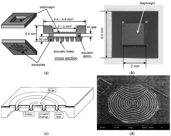
Figure 2.
(a,b) The schematic and top view of fabricated flat diaphragm, respectively, from Goto et al. [82]. (c,d) show the schematic and SEM image of corrugated diaphragm from Chen et al. [66].
3.3. Stress of the Diaphragm
In essence, the stress of the diaphragm depends on the choice of materials. Developers favor tensile over compressive stress for higher sensitivity. Miao et al. [67] suggested that it could be tuned by monitoring the process parameters during the fabrications of diaphragm, such as higher annealing temperature and lower base pressure. Some groups employed implantation method on the material, for example N2 ion [36], boron ion [42,56,73], and phosphorous ion [27,88]. These ion implantation changes the stress gradient of the diaphragm due to the mismatch between the coefficients of thermal expansions (CTE) of each material.
The second method to reduce stress is by patterning the diaphragm, as detailed in Section 3.2. The third method is by utilizing spring to suspend the acoustic diaphragm from the body. The conventional designers use edged-clamped diaphragms. The ability of the diaphragm to deflect is determined from its effective spring constant (k). The value of k can be determined from the deflection of the diaphragm using Equation (6) [56]:
where is tensile stress in Pascal (Pa), and is the diaphragm thickness in meter (m). Several groups attached spring(s) or hinge between their diaphragms and the backplates. It enables the diaphragm to have greater flexibility to release and absorb stress. This method were proposed by Weigold et al. [79], Kim et al. [81], and Mohammad et al. [97], among others.
4. Backplate and Back Chamber
The second most important parts of MEMS microphone are the backplate and back chamber. They determine the dimension of the prototype and the distance of air gap with the acoustic diaphragm. In addition, there must be outlet valve to control the air damping inside the chamber. It should be mentioned that the latest design from two groups, i.e., Lo et al. [113] and Mao et al. [118], introduced MEMS capacitive microphone without a backplate. In this structure, the perforated diaphragm and its substrate are the top and bottom plates, respectively.
Nevertheless, most groups follow the conventional structure, which necessitates this section. In Section 4.1, we describe the type of materials that are being used to make backplate and the justification for choosing them. Then, the next two sub-sections discuss the mechanisms to reduce the effect of air damping. Section 4.2 highlights works that etched acoustic holes onto their backplate, while Section 4.3 discusses two works that increased the volume of their back chambers. After that, Section 4.4 discusses air gap and efforts by several groups to study its effect to the sensitivity of their devices. We also highlight the initiative by one group that created “stopper” to avoid the diaphragm and backplate from touching each other. Finally, Section 4.5 briefly covers the materials that were chosen as the electrodes.
4.1. Backplate Materials
The capacitance of the microphone (C) is determined by the ratio of charge (Q) and bias voltage (V) being applied on both plates. Clearly, the types of material play an important role in order to produce sufficient Q. Metal is the best conductor, but semiconductor materials are an abundance in MEMS fabrication processes. The positively charged diaphragm (p-type semiconductor) and negatively charged backplate (n-type semiconductor) act as positive and negative terminals, respectively. Therefore, as can be seen from Table 1, most researchers employed Si and poly-Si as backplate material [39,43,47,67,88,95]. Few groups did opt for metals instead. For example, Buhrdorf et al. [55] employed perforated nickel (Ni), and Kabir et al. [54] proposed perforated gold (Au) for their backplates.
4.2. Acoustic Holes
Table 1 states that most research groups had perforated backplates to reduce the air-streaming resistance due to vibration being induced by the movable diaphragm. This is accomplished by etching acoustic holes on that plate. It should be mentioned that the same effect could be accomplished by etching the holes in the diaphragm. For example, Ganji et al. [91,131] did that on Al diaphragm. However, majority of groups prefer to etch backplate as it is thicker, and therefore easier to pattern. We would like to highlight one good design example from Iguchi et al. [83]. The optical microscope photograph of their backplate is shown in Figure 3. The dimension of the square backplate is 2 × 2 mm2, and it is 50 µm thick. It can be seen from the figure that 10 µm 10 µm2 acoustic holes were systematically etched on the Si backplate. A square, instead of circular, hole is patterned due to the ease of anisotropic etching.
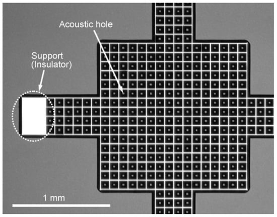
Figure 3.
Iguchi et al. [83] systematically etched 10 µm 10 µm2 acoustic holes on 2 2 mm2 Si (100) backplate.
Recent groups attempted to produce circular acoustic holes. For example, Lee et al. [116] employed a total of 1962 circular holes on the backplate that is 0.65 mm in diameter. Each hole has a radius of 4 µm.
4.3. Volume of Back Chamber
The volume of the back chamber is determined by the area of the backplate and the distance of the air gap. This space is unsealed and is filled with air. When the acoustic diaphragm vibrates due to induced pressure from the sound waves, the air inside the chamber acts as resistance and dampen the vibration, especially at high frequency. Equation (3) in Section 1 models it as mechanical resistance. One of the key parameters that determine the size of this resistance is the volume of the back chamber. As the size of back chamber increase, the effect of the air damping is reduced, as air has bigger space to travel. Few groups experimentally verified this relation. Torkkeli et al. [56] reported that, as the volume of the back chamber increased from 0.8 to 100 mm3, the sensitivity of microphone went up to 4 mV/Pa. The same effect has recently been observed by Grixti et al. [111].
4.4. Air Gap
Most of the works in Table 1 employed an insulator, such as SiO2, as an air gap. It was deposited as a sacrificial layer to form a cavity between the diaphragm and the backplate. One group did something different. Shin et al. [113] etched a Si substrate to create the air gap for their prototype. As stated by Equation (5) in Section 1, air gap between the top and bottom plates determines the open circuit sensitivity of the capacitive microphone. Table 1 shows that there is no magic number; all groups employed varying distances that suited the intended sensitivity of their prototypes. One group in particular, i.e., Tajima et al. [70], experimentally verified that air gap is inversely proportional to the sensitivity. They also found that at least 10 µm of air gap is required to achieve stable operating microphone, achieving 10 mV/Pa of sensitivity. Table 1 lists the distance of air gap for other works, as well.
If the amplitude of the induced pressure is very large, the diaphragm could touch the backplate, hence creating a short circuit between both electrodes. In order to mitigate this, Ko et al. [77] introduced stoppers on the backplate. The stopper design is shown in Figure 4.
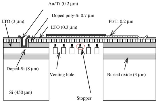
Figure 4.
Ko et al. [77] introduced a “stopper” that is attached to the backplate. In the event that the diaphragm vibrates at large amplitude, the stopper prevents it from touching the backplate.
4.5. Electrodes
The positive and negative electrodes play important role in connecting diaphragm and backplate to the output signal. Since both plates are normally made of semiconductor materials, bond pads are deposited to connect them to the electrodes. Table 1 list varieties of metals that had been chosen to function as the connector (or sometimes referred to as wire or interconnect). Al seems to be the favorite choices in majority of works, as it is in abundance and can be easily sputtered on top of the MEMS structure. Several groups opted for more expensive Au, or its variant of Ti/Au and Cr/Au, because it has higher conductivity.
5. Parameters that Determine Performances of MEMS Capacitive Microphones
The last columns in Table 1 list the key parameters that are used to measure the performances of the capacitive microphones, namely bias voltage, stray capacitance, input SPL, open circuit sensitivity, and resonant frequency. We describe them in separate sub-section here, as well as the impact that they impose on the microphone. Where possible, we give average values based on Table 1 and highlight the works of some groups that recorded extraordinary results.
5.1. Bias Voltage
The bias voltage is allegedly the easiest parameter to be modified, as Equation (5) dictates, that it is proportional to the electrical sensitivity. Unfortunately, this is not true, as increasing this parameter will eventually collapse the diaphragm to the backplate. The maximum voltage when this happens is called pull-in voltage, which is given by Equation (7):
where k is the effective spring constant of the diaphragm as given in Equation (6), is the air gap at bias voltage of zero, is the permittivity of air, and is the effective area of the diaphragm minus the acoustic holes. In order to avoid the collapse, the rule of thumb is to set the bias voltage to be one third of pull-in voltage. Two groups, i.e., Ganji et al. [87] and Kuntzman et al. [108], pushed the limit of their prototypes by using a bias voltage ≥100 V. The low values of open circuit sensitivity of 0.2 and 0.167 mV/Pa reveal their need for such high voltage. Otherwise, as can be seen in Table 1, most groups opted for more reasonable values below 20 V.
5.2. Stray Capacitance
Stray capacitance should not have been confused with the output capacitance (C) that is mentioned in Equation (1). The latter is the output that is measured from the diaphragm and backplate’s electrodes. The former is a parasitic capacitance that present between both plates to other conductive materials, such as bond pad and anchor. In the circuit model, stray capacitance is added to the measured output capacitance from the backplate, hence decreasing the accuracy of the output. Therefore, many groups attempted to minimize it. The guiding principle is to minimize the potential difference between these conductive materials and the diaphragm/backplate. As can be seen in Table 1, several groups managed to reduce the values as low as 0.2 pF [104], 0.7 pF [100], 2 pF [83], 2.12 pF [91] and 2.4 pF [106].
5.3. Input SPL
Input sound pressure level (input SPL) is the ratio between the surrounding audible sound (which is measured by sensing its pressure) and the lowest pressure that can be detected by human ears. It is given by the following equation:
where is a sound pressure, and is a reference sound pressure (20 µPa). The normal sound pressure for human speech is in the range of 60 dB SPL to 70 dB SPL, while the auditory threshold for human ears is 20 µPa (or 0 dB SPL). Researchers use input SPL to characterize the maximum pressure ( that their prototypes could detect. The input SPL column in Table 1 refers to this value. The highest recorded sound pressure was by Martin et al. [27] with the value of 164 dB SPL. The average values were around 120 dB SPL [51,52,57] and 122 dB SPL [82], while the lowest was 24 dB [60]. In some works, researchers use the standard reference input signal of 1 KHz sine wave at 94 dB input SPL (or pressure of 1 Pa) as to find the sensitivity of their microphone. For this case, 94 dB is recorded as input SPL.
5.4. Open Circuit Sensitivity
As stated by Equations (2) and (5), the open circuit sensitivity can be increased by modifying the following parameters: bias voltage, air gap, area of diaphragm, diaphragm thickness, and diaphragm stress. Looking at Table 1, the sensitivity of 10 mV/Pa seems to be a good benchmark. Section 3 and Section 4 already describe the efforts by many groups to increase the value this parameter in term of the material and topology of the diaphragm, as well as perforated backplate, volume of the back chamber, and reducing air gap. In order to avoid duplication, those strategies are not repeated here.
5.5. Resonant Frequency
The resonant frequency (fo) limits the upper bandwidth of the microphone. It is given as [132]:
where E, µ, and ρ are Young’s Modulus, Poisson’s ratio, and density of material, respectively, κ is compressibility of air, is air gap between the plates, and and a are thickness and side length of square diaphragm, respectively. Equation (8) shows that fo is affected by properties of the material and the dimension of the diaphragm. Although this equation is designed for square diaphragm, it can be used for circular diaphragm by assuming equal areas, given in Equation (9) [64]:
where a is a side length of square diaphragm, and R is a radius of circular diaphragm.
Table 1 shows the values of fo from all the works. Most researchers designed their capacitive microphone on human hearing range. Therefore, it is not surprising that most works had fo ≤ 20 kHz. For example, Martin et al. applied their microphone for aeroacoustic measurement with frequency range from 300 Hz to 20 kHz [27]. Several groups designed their prototypes as hearing aid devices with different fo, i.e., 4 kHz [80], 10 kHz [106] and 14 kHz [43].
However, several group custom-made their prototypes for different fo to cater for specific applications. For example, Hohm et al. developed their microphone to have a very low fo of 2 kHz for airborne sound detection [36]. On the other extreme, Hansen et al. proposed a capacitive micromachined ultrasonic transducers (CMUTs) at frequency range of 100 Hz to 100 kHz for the generation and reception of ultrasound in air and water [72].
5.6. Noise Floor
Another parameter that affect the performance is the noise floor. Not many groups reported this parameter in their articles, hence, it is not included in Table 1. The squeezed-film effect due to air damping is the dominant noise mechanism. For detailed explanation, readers are referred to author’ review paper on MEMS microphone [35]. The noise floor affects the minimum detectable level of induced pressure from the sound waves. The most recent technique to reduce it is by employing double diaphragms or double backplates to create a differential capacitive sensing scheme [27,46,53]. Other than that, several groups manage to reduce the noise floor with a single diaphragm and backplate by controlling the air damping. They manage to achieve the noise floor of 39 dB [64], 30.5 dB [83], 35 dB [88] and 33.5 dB [56].
6. Future Research Direction for MEMS Capacitive Microphone
What direction of research that should be pursued next? In order to answer this million-dollars question, let us take a closer look at Table 1, especially the articles that have been published in the last five years. Based on those works, we list the possibilities herein. It should be noted that the predictions are limited to MEMS-based research activities. There are other field of research that are closely related to the development of microphones, for example, signal processing and integrated circuit design. Those are not covered here.
The first direction is the employment of new materials to make the acoustic diaphragm. We have seen recent works that use graphene [115,119,125,126,128], silicon carbide (SiC) [120], and composite materials [116,127]. Graphene is employed as researchers are ‘riding on the wave’ of this material. while SiC and composite materials are chosen due to their superior mechanical properties over Si. While the employment of new materials is the easiest route for novelty in academic publishing, the high cost associated with the exotic fabrication processes discourage industries from following through. Our recommendation is for those researchers to find a niche application for their prototypes. For example, SiC could operate at higher temperature than Si. Hence, its application as an acoustic diaphragm could be targeted for an extreme environment.
The second direction is in term of design optimization. There are many recent examples. In one, Jantawong et al. [124] introduced a stepped cavity to increase the value of the output capacitance. In another, Ganji group are pursuing the hinge or spring design to reduce the residual stress of the diaphragm [121,123]. Gharaei et al. [26] proposed a fungous coupled diaphragm to decrease the dependence of sensitivity to the effective area. In addition, two groups reported the structure that did not need a dedicated backplate [113,118]. With the wider availability of design tools in universities, we expect this direction to flourish. It should be noted, however, that design optimization is considered to be of low impact, hence published works rarely appearing in top journals. There is a way to overcome this obstacle. If those researchers combine the design optimization with better and accurate modeling of the device [133,134], the impact of their works will be bigger.
For the third direction, we have seen attempts to integrate the mechanical and electrical modules together. At stated in Section 1, Kuhnel et al. [33] and Graf et al. [34] pioneered this in early 1990s. However, their works were not followed through due to the high noise floor. Recently, we have seen publications that attempted to solve this problem [114,135,136], with some groups promoting CMOS-MEMS process [134,136] as the best solution to accomplish this goal. If these solutions are practical and proven to reduce the level of noise floor, this direction of research will be a gold mine for industry, as it pushes the cost and footprint lower.
The fourth direction is on the comprehensive testing of the prototypes. In the past, academic researchers are less interested with this direction as it is considered to be of low novelty. In industry, however, it is the opposite, as they could not release the products without passing these mandatory test procedures. Recently, we have seen two groups that are pursuing this direction. Nicollini et al. [122] developed a MEMS microphone based on a poly-Si diaphragm. They conducted comprehensive acoustical, electrical, and thermal tests to demonstrate the capabilities of their prototype. In another work, Lu et al. [134] performed comprehensive thermal test on their CMOS-MEMS microphone. Their prototype was fabricated on the Taiwan Semiconductor Manufacturing Corporation (TSMC) 0.18u process, using three aluminum layers as the diaphragm, spring, and backplate. Both recent publications are an encouraging sign. We believe that future academic works should pay more attention to proper testing of their prototypes, in particular on the reliability and repeatability aspects.
Finally, one would wonder if academia and industry are sharing similar “wish lists” for the future directions of MEMS capacitive microphone’s research activities. Therefore, we refer to Wang et al. [136], in which they present an industry view on this subject during TRANSDUCERS 2015. It is not surprising that most of the points are similar to the ones that are covered in this review. Furthermore, they emphasized a few additional items. First, the fabrication strategies to deposit non-sticking and low residual stress diaphragm. Second, the development of on-die microphones arrays to increase the signal-to-noise ratio. Third, the design of the package with shutter to protect the microphone from shock, high pressure, ESD etc. As industry prefers to patent their inventions, academic researchers should take the opportunity to publish their works on these issues.
7. Conclusions
MEMS capacitive microphone has been developed since 1980s. After 30 years, it still garners considerable interests in academia. The continuing attention for this device is fueled by its commercial successes. The best success story is the integration of MEMS capacitive microphone inside smart phones, as well as other IoT devices for audio and other sensing applications. We recommend academic researchers to align their future works with industry’s requirement to further develop this versatile device.
Author Contributions
Conceptualization, F.M.-Y.; data curation, S.A.Z., formal analysis, S.A.Z. and F.M.-Y.; writing—original draft preparation, S.A.Z. and A.A.H.; writing—review and editing, F.M.-Y.; supervision, F.M.-Y., A.A.H. and B.Y.M.; project administration, F.M.-Y., A.A.H. and B.Y.M.; funding acquisition, F.M.-Y., A.A.H. and B.Y.M. All authors have read and agreed to the published version of the manuscript.
Funding
This research was funded by IRU-MRUN COLLABORATIVE RESEARCH PROGRAMME, grant numbers MRUN-2015-004 (Universiti Kebangsaan Malaysia) and 218997 (Griffith University).
Acknowledgments
This work was performed in part at the Queensland node of the Australian National Fabrication Facility, a company established under the National Collaborative Research Infrastructure Strategy to provide nano- and micro-fabrication facilities for Australia’s researchers.
Conflicts of Interest
The authors declare no conflict of interest.
References
- Arya, D.S.; Prasad, M.; Tripathi, C.C. Design and modeling of a ZnO-based MEMS acoustic sensor for aeroacoustic and audio applications. In Proceedings of the 2015 2nd International Symposium on Physics and Technology of Sensors (ISPTS), Pune, India, 7–10 March 2015; IEEE: Piscataway, NJ, USA, 2015. [Google Scholar]
- Loeppert, P.V.; Lee, S.B. A commercialized MEMS microphone for high-volume consumer electronics. J. Acoust. Soc. Am. 2004, 116, 2510. [Google Scholar] [CrossRef]
- Mallik, S.; Chowdhury, D.; Chattopadhyay, M. Development and performance analysis of a low-cost MEMS microphone-based hearing aid with three different audio amplifiers. Innov. Syst. Softw. Eng. 2019, 15, 17–25. [Google Scholar] [CrossRef]
- Zargarpour, N.; Zarifi, M.H. A piezoelectric micro-electromechanical microphone for implantable hearing aid applications. Microsyst. Technol. 2015, 21, 893–902. [Google Scholar] [CrossRef]
- Marek, J. MEMS for automotive and consumer electronics. In Proceedings of the 2010 IEEE International Solid-State Circuits Conference—(ISSCC), San Francisco, CA, USA, 7–11 February 2010; IEEE: Piscataway, NJ, USA, 2010. [Google Scholar]
- Zinserling, B. Silicon-based MEMS microphone for automotive applications. Micronano News. 2007. Available online: www.onboard-technology.com/pdf_febbraio2007/020705.pdf (accessed on 7 May 2020).
- MacLeod, E. Alexander Graham Bell: An Inventive Life; Kids Can Press: Toronto, ON, Canada, 1999. [Google Scholar]
- Huurdeman, A.A. The Worldwide History of Telecommunications; John Wiley & Sons: Hoboken, NJ, USA, 2003. [Google Scholar]
- Malcovati, P.; Grassi, M.; Baschirotto, A. Interface Circuits for MEMS Microphones. In Nyquist AD Converters, Sensor Interfaces, and Robustness: Advances in Analog Circuit Design, 2012; van Roermund, A.H.M., Baschirotto, A., Steyaert, M., Eds.; Springer: New York, NY, USA, 2013; pp. 149–174. [Google Scholar]
- Elko, G.W. Future Directions for Microphone Arrays. In Microphone Arrays: Signal Processing Techniques and Applications; Brandstein, M., Ward, D., Eds.; Springer: Berlin, Heidelberg, Germany, 2001; pp. 383–387. [Google Scholar]
- Eargle, J. The Microphone Book; Elsevier: Amsterdam, The Netherlands, 2005. [Google Scholar]
- Horng, R.-H.; Chen, K.-F.; Tsai, Y.-C.; Suen, C.-Y.; Chang, C.-C. Fabrication of a dual-planar-coil dynamic microphone by MEMS techniques. J. Micromech. Microeng. 2010, 20, 065004. [Google Scholar] [CrossRef]
- Lee, C.-I.; Chien, H.-T.; Liu, P.-T.; Chen, J.M. High sensitivity silicon-based condenser microphone design. In Proceedings of the 2007 International Microsystems, Packaging, Assembly and Circuits Technolog, Taipei, Taiwan, 1–3 October 2007; IEEE: Piscataway, NJ, USA, 2007. [Google Scholar]
- Ried, R.; Kim, E.S.; Hong, D.; Muller, R. Piezoelectric microphone with on-chip CMOS circuits. J. Microelectromech. Syst. 1993, 2, 111–120. [Google Scholar] [CrossRef]
- Fuji, Y.; Higashi, Y.; Masunishi, K.; Yuzawa, A.; Nagata, T.; Kaji, S.; Okamoto, K.; Baba, S.; Ono, T.; Hara, M. Spin-MEMS microphone integrating a series of magnetic tunnel junctions on a rectangular diaphragm. J. Appl. Phys. 2018, 123, 163901. [Google Scholar] [CrossRef]
- Fuji, Y.; Hara, M.; Higashi, Y.; Kaji, S.; Masunishi, K.; Nagata, T.; Yuzawa, A.; Otsu, K.; Okamoto, K.; Baba, S.; et al. An ultra-sensitive spintronic strain-gauge sensor with gauge factor of 5000 and demonstration of a Spin-MEMS Microphone. In Proceedings of the 2017 19th International Conference on Solid-State Sensors, Actuators and Microsystems (TRANSDUCERS), Kaohsiung, Taiwan, 18–22 June 2017; IEEE: Piscataway, NJ, USA, 2017. [Google Scholar]
- Higashi, Y.; Fuji, Y.; Kaji, S.; Masunishi, K.; Nagata, T.; Yuzawa, A.; Otsu, K.; Okamoto, K.; Baba, S.; Ono, T.; et al. SNR enhancement of a spin-MEMS microphone by optimum bias magnetic field and demonstration of operation sound monitoring of rotating equipment. In Proceedings of the 2018 IEEE Micro Electro Mechanical Systems (MEMS), Belfast, UK, 21–25 January 2018; IEEE: Piscataway, NJ, USA, 2018. [Google Scholar]
- Fuji, Y.; Higashi, Y.; Kaji, S.; Masunishi, K.; Nagata, T.; Yuzawa, A.; Okamoto, K.; Baba, S.; Ono, T.; Hara, M. Highly sensitive spintronic strain-gauge sensor and Spin-MEMS microphone. Jpn. J. Appl. Phys. 2019, 58, SD0802. [Google Scholar] [CrossRef]
- Van Rhijn, A. Integrated Circuits for High-Performance Electret Microphones; Penton Media, Inc.: New York, NY, USA, 2003; p. 38. [Google Scholar]
- Del Val, L.; Izquierdo, A.; Villacorta, J.J.; Suárez, L.; Suá Rez, L. Using a Planar Array of MEMS Microphones to Obtain Acoustic Images of a Fan Matrix. J. Sensors 2017, 2017, 1–10. [Google Scholar] [CrossRef]
- Izquierdo, A.; Villacorta, J.J.; Del Val, L.; Suárez, L.; Suárez, D. Implementation of a Virtual Microphone Array to Obtain High Resolution Acoustic Images. Sensors 2017, 18, 25. [Google Scholar] [CrossRef]
- Zhang, X.; Huang, J.; Song, E.; Liu, H.; Li, B.; Yuan, X. Design of Small MEMS Microphone Array Systems for Direction Finding of Outdoors Moving Vehicles. Sensors 2014, 14, 4384–4398. [Google Scholar] [CrossRef]
- Johnson, R.C. MEMS Mics Taking Over. In EE Times; Aspencore: New York, NY, USA, 2014. [Google Scholar]
- Bouchaud, J.; Boustany, M. MEMS Market Tracker—Consumer and Mobile; IHS: London, UK, 2014. [Google Scholar]
- Dixon-Warren, S. Overview of MEMS Microphone Technologies for Consumer Applications; Mems Journal Inc.: Southfield, MI, USA, 2011. [Google Scholar]
- Gharaei, H.; Koohsorkhi, J. Design and characterization of high sensitive MEMS capacitive microphone with fungous coupled diaphragm structure. Microsyst. Technol. 2016, 22, 401–411. [Google Scholar] [CrossRef]
- Martin, D.T.; Liu, J.; Kadirvel, K.; Fox, R.M.; Sheplak, M.; Nishida, T. A Micromachined Dual-Backplate Capacitive Microphone for Aeroacoustic Measurements. J. Microelectromech. Syst. 2007, 16, 1289–1302. [Google Scholar] [CrossRef]
- Kim, B.-H.; Lee, H.-S. Acoustical-Thermal Noise in a Capacitive MEMS Microphone. IEEE Sens. J. 2015, 15, 6853–6860. [Google Scholar] [CrossRef]
- Scheeper, P.; Van Der Donk, A.; Olthuis, W.; Bergveld, P. A review of silicon microphones. Sens. Actuators A Phys. 1994, 44, 1–11. [Google Scholar] [CrossRef]
- Ishfaque, A.; Kim, B. Fly Ormia Ochracea Inspired MEMS Directional Microphone: A Review. IEEE Sens. J. 2018, 18, 1778–1789. [Google Scholar] [CrossRef]
- Miles, R.N. Mechanically coupled ears for directional hearing in the parasitoid fly Ormia ochracea. J. Acoust. Soc. Am. 1995, 98, 3059–3070. [Google Scholar] [CrossRef] [PubMed]
- Shah, M.A.; Shah, I.A.; Lee, D.-G.; Hur, S. Design Approaches of MEMS Microphones for Enhanced Performance. J. Sens. 2019, 2019, 1–26. [Google Scholar] [CrossRef]
- Kühnel, W. Silicon condenser microphone with integrated field-effect transistor. Sens. Actuators A Phys. 1991, 26, 521–525. [Google Scholar] [CrossRef]
- Graf, E.; Kronast, W.; Dühring, S.; Muller, B.; Stoffel, A. Silicon membrane condenser microphone with integrated field-effect transistor. Sens. Actuators A Phys. 1993, 37, 708–711. [Google Scholar] [CrossRef]
- Mohd-Yasin, F.; Nagel, D.J.; E Korman, C. Noise in MEMS. Meas. Sci. Technol. 2009, 21, 12001. [Google Scholar] [CrossRef]
- Hohm, D. A subminiature condenser microphone with silicon nitride membrane and silicon back plate. J. Acoust. Soc. Am. 1989, 85, 476–480. [Google Scholar] [CrossRef]
- Bergqvist, J.; Rudolf, F. A new condenser microphone in silicon. Sens. Actuators A Phys. 1990, 21, 123–125. [Google Scholar] [CrossRef]
- Kühnel, W.; Hess, G. A silicon condenser microphone with structured back plate and silicon nitride membrane. Sens. Actuators A Phys. 1992, 30, 251–258. [Google Scholar] [CrossRef]
- Scheeper, P.; Van Der Donk, A.; Olthuis, W.; Bergveld, P. Fabrication of silicon condenser microphones using single wafer technology. J. Microelectromech. Syst. 1992, 1, 147–154. [Google Scholar] [CrossRef]
- Bourouina, T.; Spirkovitch, S.; Baillieu, F.; Vauge, C. A new condenser microphone with a p+ silicon membrane. Sens. Actuators A Phys. 1992, 31, 149–152. [Google Scholar] [CrossRef]
- Bergqvist, J.; Rudolf, F. A silicon condenser microphone using bond and etch-back technology. Sens. Actuators A Phys. 1994, 45, 115–124. [Google Scholar] [CrossRef]
- Bergqvist, J.; Gobet, J. Capacitive microphone with a surface micromachined backplate using electroplating technology. J. Microelectromech. Syst. 1994, 3, 69–75. [Google Scholar] [CrossRef]
- Scheeper, P.; Olthuis, W.; Bergveld, P. Improvement of the performance of microphones with a silicon nitride diaphragm and backplate. Sens. Actuators A Phys. 1994, 40, 179–186. [Google Scholar] [CrossRef]
- Schellin, R.; Hess, G.; Kühnel, W.; Thielemann, C.; Trost, D.; Wacker, J.; Steinmann, R. Measurements of the mechanical behaviour of micromachined silicon and silicon-nitride membranes for microphones, pressure sensors and gas flow meters. Sens. Actuators A Phys. 1994, 41, 287–292. [Google Scholar] [CrossRef]
- Van Der Donk, A.; Scheeper, P.; Olthuis, W.; Bergveld, P. Modelling of silicon condenser microphones. Sens. Actuators A Phys. 1994, 40, 203–216. [Google Scholar] [CrossRef]
- Bay, J.; Hansen, O.; Bouwstra, S. Design of a silicon microphone with differential read-out of a sealed double parallel-plate capacitor. Sens. Actuators A Phys. 1996, 53, 232–236. [Google Scholar] [CrossRef]
- Ning, Y.; Mitchell, A.; Tait, R. Fabrication of a silicon micromachined capacitive microphone using a dry-etch process. Sens. Actuators A Phys. 1996, 53, 237–242. [Google Scholar] [CrossRef]
- Zou, Q.; Li, Z.; Liu, L. Design and fabrication of silicon condenser microphone using corrugated diaphragm technique. J. Microelectromech. Syst. 1996, 5, 197–204. [Google Scholar]
- Thielemann, C.; Hess, G. Inorganic electret membrane for a silicon microphone. Sens. Actuators A Phys. 1997, 61, 352–355. [Google Scholar] [CrossRef]
- Hsu, P.-C.; Mastrangelo, C.H.; Wise, K.D. A high sensitivity polysilicon diaphragm condenser microphone. In Proceedings of the MEMS 98. IEEE. Eleventh Annual International Workshop on Micro Electro Mechanical Systems. An Investigation of Micro Structures, Sensors, Actuators, Machines and Systems (Cat. No.98CH36176), Heidelberg, Germany, 25–29 January 1998; IEEE: Piscataway, NJ, USA, 1998. [Google Scholar]
- Pederson, M.; Olthuis, W.; Bergveld, P. High-performance condenser microphone with fully integrated CMOS amplifier and DC-DC voltage converter. J. Microelectromech. Syst. 1998, 7, 387–394. [Google Scholar] [CrossRef]
- Pedersen, M.; Olthuis, W.; Bergveld, P. An integrated silicon capacitive microphone with frequency-modulated digital output. Sens. Actuators A Phys. 1998, 69, 267–275. [Google Scholar] [CrossRef]
- Bay, J.; Hansen, O.; Bouwstra, S. Micromachined double backplate differential capacitive microphone. J. Micromech. Microeng. 1999, 9, 30–33. [Google Scholar] [CrossRef]
- Kabir, A.; Bashir, R.; Bernstein, J.; De Santis, J.; Mathews, R.; O’Boyle, J.; Bracken, C. High sensitivity acoustic transducers with thin p+ membranes and gold back-plate. Sens. Actuators A Phys. 1999, 78, 138–142. [Google Scholar] [CrossRef]
- Buhrdorf, A.; Tebje, L.; Ahrens, O.; Glitza, O.; Binder, J. Capacitive micromachined ultrasonic transducer (cMUT) array for the frequency range below 500 kHz In Proceedings of the 2000 IEEE Ultrasonics Symposium. In Proceedings of the An International Symposium (Cat. No.00CH37121), San Juan, PR, USA, 22–25 October 2000; IEEE: Piscataway, NJ, USA, 2000. [Google Scholar]
- Torkkeli, A.; Rusanen, O.; Saarilahti, J.; Seppä, H.; Sipola, H.; Hietanen, J. Capacitive microphone with low-stress polysilicon membrane and high-stress polysilicon backplate. Sens. Actuators A Phys. 2000, 85, 116–123. [Google Scholar] [CrossRef]
- Brauer, M.; Dehé, A.; Bever, T.; Barzen, S.; Schmitt, S.; Füldner, M.; Aigner, R. Silicon microphone based on surface and bulk micromachining. J. Micromech. Microeng. 2001, 11, 319–322. [Google Scholar] [CrossRef]
- Hansen, S.; Ergun, A.S.; Khuri-Yakub, B. Acoustic sensing using radio frequency detection and capacitive micromachined ultrasonic transducers. In Proceedings of the 2001 IEEE MTT-S International Microwave Sympsoium Digest (Cat. No.01CH37157), Phoenix, AZ, USA, 20–24 May 2001; IEEE: Piscataway, NJ, USA, 2001. [Google Scholar]
- Li, X.; Lin, R.; Kek, H.; Miao, J.; Zou, Q. Sensitivity-improved silicon condenser microphone with a novel single deeply corrugated diaphragm. Sens. Actuators A Phys. 2001, 92, 257–262. [Google Scholar] [CrossRef]
- Müllenborn, M.; Rombach, P.; Klein, U.; Rasmussen, K.; Kuhmann, J.; Heschel, M.; Gravad, M.; Janting, J.; Branebjerg, J.; Hoogerwerf, A.; et al. Chip-size-packaged silicon microphones. Sens. Actuators A Phys. 2001, 92, 23–29. [Google Scholar] [CrossRef]
- Noble, R.; Jones, A.; Robertson, T.; Hutchins, D.A.; Billson, D. Novel, wide bandwidth, micromachined ultrasonic transducers. IEEE Trans. Ultrason. Ferroelectr. Freq. Control. 2001, 48, 1495–1507. [Google Scholar] [CrossRef] [PubMed]
- Kronast, W.; Müller, B.; Siedel, W.; Stoffel, A. Single-chip condenser microphone using porous silicon as sacrificial layer for the air gap. Sens. Actuators A Phys. 2001, 87, 188–193. [Google Scholar] [CrossRef]
- Rombach, P.; Müllenborn, M.; Klein, U.; Rasmussen, K. The first low voltage, low noise differential silicon microphone, technology development and measurement results. Sens. Actuators A Phys. 2002, 95, 196–201. [Google Scholar] [CrossRef]
- Kressmann, R.; Klaiber, M.; Hess, G. Silicon condenser microphones with corrugated silicon oxide/nitride electret membranes. Sens. Actuators A Phys. 2002, 100, 301–309. [Google Scholar] [CrossRef]
- Sim, W.; Kim, B.; Choi, B.; Park, J.-O. Thermal and load-deflection FE analysis of Parylene Diaphragms. In Proceedings of the Modelling and Simulation of Microsystems Conference, San Juan, PR, USA, 22–25 April 2002. [Google Scholar]
- Chen, J.; Liu, L.; Li, Z.; Tan, Z.; Xu, Y.; Ma, J. Single-chip condenser miniature microphone with a high sensitive circular corrugated diaphragm. In Proceedings of the Technical Digest. MEMS 2002 IEEE International Conference. Fifteenth IEEE International Conference on Micro Electro Mechanical Systems (Cat. No.02CH37266), Las Vegas, NV, USA, 24 January 2002; IEEE: Piscataway, NJ, USA, 2002. [Google Scholar]
- Miao, J.; Lin, R.; Chen, L.; Zou, Q.; Lim, S.Y.; Seah, S.H. Design considerations in micromachined silicon microphones. Microelectron. J. 2002, 33, 21–28. [Google Scholar] [CrossRef]
- Chen, J.; Liu, L.; Li, Z.; Tan, Z.; Xu, Y.; Ma, J. On the single-chip condenser miniature microphone using DRIE and backside etching techniques. Sens. Actuators A Phys. 2003, 103, 42–47. [Google Scholar] [CrossRef]
- Scheeper, P.; Nordstrand, B.; Gullov, J.; Liu, B.; Clausen, T.; Midjord, L.; Storgaard-Larsen, T.; Gullv, J. A new measurement microphone based on MEMS technology. J. Microelectromech. Syst. 2003, 12, 880–891. [Google Scholar] [CrossRef]
- Tajima, T.; Nishiguchi, T.; Chiba, S.; Morita, A.; Abe, M.; Tanioka, K.; Saito, N.; Esashi, M. High-performance ultra-small single crystalline silicon microphone of an integrated structure. Microelectron. Eng. 2003, 67, 508–519. [Google Scholar] [CrossRef]
- Wang, W.J.; Lin, R.M.; Li, X.; Guo, D.G. Study of single deeply corrugated diaphragms for high-sensitivity microphones. J. Micromech. Microeng. 2002, 13, 184–189. [Google Scholar] [CrossRef]
- Hansen, S.T.; Ergün, A.S.; Liou, W.; Auld, B.A.; Khuri-Yakub, B.T. Wideband micromachined capacitive microphones with radio frequency detection. J. Acoust. Soc. Am. 2004, 116, 828–842. [Google Scholar] [CrossRef]
- Ning, J.; Liu, Z.; Liu, H.; Ge, Y. A silicon capacitive microphone based on oxidized porous silicon sacrificial technology. In Proceedings of the 7th International Conference on Solid-State and Integrated Circuits Technology, Beijing, China, 18–21 October 2004. [Google Scholar]
- Wang, W.J.; Lin, R.M.; Zou, Q.B.; Li, X.X. Modeling and characterization of a silicon condenser microphone. J. Micromech. Microeng. 2003, 14, 403–409. [Google Scholar] [CrossRef]
- Wang, W.J.; Lin, R.M.; Ren, Y. Design and fabrication of high sensitive microphone diaphragm using deep corrugation technique. Microsyst. Technol. 2004, 10, 142–146. [Google Scholar] [CrossRef]
- Sezen, A.S.; Sivaramakrishnan, S.; Hur, S.; Rajamani, R.; Robbins, W.; Nelson, B.J. Passive Wireless MEMS Microphones for Biomedical Applications. J. Biomech. Eng. 2005, 127, 1030–1034. [Google Scholar] [CrossRef] [PubMed][Green Version]
- Ko, S.C.; Jun, C.; Jang, W.I.; Choi, C.-A. Micromachined air-gap structure MEMS acoustic sensor using reproducible high-speed lateral etching and CMP process. J. Micromech. Microeng. 2006, 16, 2071–2076. [Google Scholar] [CrossRef]
- Kim, H.-J.; Lee, S.Q.; Park, K.H. A novel capacitive type miniature microphone with a flexure hinge diaphragm. Optics East 2006, 6374, 63740. [Google Scholar]
- Weigold, J.; Brosnihan, T.; Bergeron, J.; Zhang, X. A MEMS Condenser Microphone for Consumer Applications. In Proceedings of the 19th IEEE International Conference on Micro Electro Mechanical Systems, Istanbul, Turkey, 22–26 January 2006; pp. 86–89. [Google Scholar]
- Dehé, A. Silicon microphone development and application. Sens. Actuators A Phys. 2007, 133, 283–287. [Google Scholar] [CrossRef]
- Kim, H.-J.; Lee, J.W.; Lee, S.Q.; Lee, S.K.; Park, K.H. A Miniature Condenser Microphone for Portable Terminals Applications. Sensors 2007. [CrossRef]
- Goto, M.; Iguchi, Y.; Ono, K.; Ando, A.; Takeshi, F.; Matsunaga, S.; Yasuno, Y.; Tanioka, K.; Tajima, T. High-Performance Condenser Microphone With Single-Crystalline Silicon Diaphragm and Backplate. IEEE Sens. J. 2006, 7, 4–10. [Google Scholar] [CrossRef]
- Iguchi, Y.; Goto, M.; Iwaki, M.; Ando, A.; Tanioka, K.; Tajima, T.; Takeshi, F.; Matsunaga, S.; Yasuno, Y. Silicon microphone with wide frequency range and high linearity. Sens. Actuators A Phys. 2007, 135, 420–425. [Google Scholar] [CrossRef]
- Kwon, H.-S.; Lee, K.-C. Double-chip condenser microphone for rigid backplate using DRIE and wafer bonding technology. Sens. Actuators A Phys. 2007, 138, 81–86. [Google Scholar] [CrossRef]
- Kasai, T.; Tsurukame, Y.; Takahashi, T.; Sato, F.; Horiike, S. Small Silicon Condenser Microphone Improved with a Backchamber with Concave Lateral Sides. In Proceedings of the TRANSDUCERS 2007-2007 International Solid-State Sensors, Actuators and Microsystems Conference, Lyon, France, 10–14 June 2007; pp. 2613–2616. [Google Scholar]
- Chen, J.-Y.; Hsu, Y.-C.; Lee, S.-S.; Mukherjee, T.; Fedder, G.K. Modeling and simulation of a condenser microphone. Sens. Actuators A Phys. 2008, 145, 224–230. [Google Scholar] [CrossRef]
- Ganji, B.A.; Majlis, B.Y. Deposition and etching of diaphragm and sacrificial layer in novel MEMS capacitive microphone structure. In Proceedings of the 2008 IEEE International Conference on Semiconductor Electronics, Johor Bahru, Malaysia, 25–27 November 2008. [Google Scholar]
- Her, H.-C.; Wu, T.-L.; Huang, J.H. Acoustic analysis and fabrication of microelectromechanical system capacitive microphones. J. Appl. Phys. 2008, 104, 84509. [Google Scholar] [CrossRef]
- Hall, N.A.; Okandan, M.; Littrell, R.; Bicen, B.; Degertekin, F.L. Simulation of Thin-Film Damping and Thermal Mechanical Noise Spectra for Advanced Micromachined Microphone Structures. J. Microelectromech. Syst. 2008, 17, 688–697. [Google Scholar] [CrossRef] [PubMed]
- Kaur, M.C.; Pratap, R.; Bhat, N. Design of a high sensitivity FET integrated MEMS microphone. Procedia Chem. 2009, 1, 875–878. [Google Scholar] [CrossRef]
- Ganji, B.A.; Majlis, B.Y. Design and fabrication of a new MEMS capacitive microphone using a perforated aluminum diaphragm. Sens. Actuators A Phys. 2009, 149, 29–37. [Google Scholar] [CrossRef]
- Ganji, B.A.; Majlis, B.Y. High sensitivity and small size MEMS capacitive microphone using a novel slotted diaphragm. Microsyst. Technol. 2009, 15, 1401–1406. [Google Scholar] [CrossRef]
- Lee, J.; Ko, S.; Je, C.; Lee, M.; Choi, C.-A.; Yang, Y.; Heo, S.; Kim, J. A surface-micromachined MEMS acoustic sensor with X-shape bottom electrode anchor. Sensors 2009. [Google Scholar] [CrossRef]
- Leinenbach, C.; Van Teeffelen, K.; Laermer, F.; Seidel, H. A new capacitive type MEMS microphone. In Proceedings of the 2010 IEEE 23rd International Conference on Micro Electro Mechanical Systems (MEMS), Wanchai, Hong Kong, China, 24–28 January 2010. [Google Scholar]
- Ganji, B.A.; Majlis, B.Y. Slotted capacitive microphone with sputtered aluminum diaphragm and photoresist sacrificial layer. Microsyst. Technol. 2010, 16, 1803–1809. [Google Scholar] [CrossRef]
- Yang, C.-T. The sensitivity analysis of a MEMS microphone with different membrane diameters. J. Mar. Sci. Technol. 2010, 18, 790–796. [Google Scholar]
- Mohamad, N. Design of Spring-Supported Diaphragm Capacitive MEMS Microphone. Ph.D. Thesis, Swinburne University of Technology, Victoria, Australia, November 2016. [Google Scholar]
- Chan, C.K.; Lai, W.C.; Wu, M.; Wang, M.Y.; Fang, W. Design and Implementation of a Capacitive-type Microphone with Rigid Diaphragm and Flexible Spring Using the Two Poly Silicon Micromachining Processes. IEEE Sens. J. 2011, 11, 2365–2371. [Google Scholar] [CrossRef]
- Chiang, C.-T.; Wu, C.-Y. A CMOS Digitized Silicon Condenser Microphone for Acoustic Applications. IEEE Sens. J. 2011, 11, 296–304. [Google Scholar] [CrossRef]
- Huang, C.-H.; Lee, C.-H.; Hsieh, T.-M.; Tsao, L.-C.; Wu, S.; Liou, J.-C.; Wang, M.-Y.; Chen, L.-C.; Yip, M.-C.; Fang, W. Implementation of the CMOS MEMS Condenser Microphone with Corrugated Metal Diaphragm and Silicon Back-Plate. Sensors 2011, 11, 6257–6269. [Google Scholar] [CrossRef] [PubMed]
- Jawed, S.A.; Cattin, D.; Gottardi, M.; Massari, N.; Baschirotto, A.; Simoni, A. A 828μW 1.8V 80dB dynamic-range readout interface for a MEMS capacitive microphone. In Proceedings of the ESSCIRC 2008—34th European Solid-State Circuits Conference, Edinburgh, UK, 15–19 September 2008. [Google Scholar]
- Je, C.H.; Lee, J.; Yang, W.S.; Kim, J. The Novel Sensitivity Improved Surface Micromachined MEMS Microphone with the Center-Hole Membrane. Procedia Eng. 2011, 25, 583–586. [Google Scholar] [CrossRef]
- Kasai, T.; Sato, S.; Conti, S.; Padovani, I.; David, F.; Uchida, Y.; Takahashi, T.; Nishio, H. Novel concept for a MEMS microphone with dual channels for an ultrawide dynamic range. In Proceedings of the 2011 IEEE 24th International Conference on Micro Electro Mechanical Systems, Cancun, Mexico, 23–27 January 2011. [Google Scholar]
- Lee, J.; Je, C.; Yang, W.; Kim, J. Structure-based equivalent circuit modeling of a capacitive-type MEMS microphone. In Proceedings of the 2012 International Symposium on Communications and Information Technologies (ISCIT), Gold Coast, QLD, Australia, 2–5 October 2012. [Google Scholar]
- Ahmadnejad, J.; Ganji, B.A.; Nemati, A.; Nemati, A. Design, analysis, and modelling of a MEMS capacitive microphone for integration into CMOS circuits. In Proceedings of the 2013 IEEE Asia Pacific Conference on Postgraduate Research in Microelectronics and Electronics (PrimeAsia), Visakhapatnam, India, 19–21 December 2013. [Google Scholar]
- Chao, P.C.-P.; Tsai, C.-Y.; Chiu, C.-W.; Tsai, C.-H.; Tu, T.-Y. A new hybrid fabrication process for a high sensitivity MEMS microphone. Microsyst. Technol. 2013, 19, 1425–1431. [Google Scholar] [CrossRef]
- Je, C.H.; Lee, J.; Yang, W.S.; Kwon, J.-K. A surface micromachined MEMS capacitive microphone with back-plate supporting pillars. In SENSORS, 2013 IEEE; IEEE: Piscataway, NJ, USA, 2013. [Google Scholar]
- Kuntzman, M.L.; Hall, N.A. A broadband, capacitive, surface-micromachined, omnidirectional microphone with more than 200 kHz bandwidth. J. Acoust. Soc. Am. 2014, 135, 3416–3424. [Google Scholar] [CrossRef]
- Lee, Y.H.; Jung, Y.D.; Kwak, J.-H.; Hur, S. Design and Fabrication of One-Chip MEMS Microphone for the Hearing Impaired. Appl. Mech. Mater. 2014, 461, 577–580. [Google Scholar] [CrossRef]
- Lee, Y.H.; Jung, Y.; Kwak, J.-H.; Hur, S. Development of capacitive-type MEMS microphone with CMOS amplifying chip. Int. J. Precis. Eng. Manuf. 2014, 15, 1423–1427. [Google Scholar] [CrossRef]
- Grixti, R.; Grech, I.; Casha, O.; Darmanin, J.M.; Gatt, E.; Micallef, J. Analysis and design of an electrostatic MEMS microphone using the PolyMUMPs process. Analog. Integr. Circuits Signal Process. 2015, 82, 599–610. [Google Scholar] [CrossRef]
- Kuntzman, M.L.; Kim, D.; Hall, N.A. Microfabrication and Experimental Evaluation of a Rotational Capacitive Micromachined Ultrasonic Transducer. J. Microelectromech. Syst. 2014, 24, 404–413. [Google Scholar] [CrossRef]
- Lo, S.-C.; Lai, W.-C.; Chang, C.-I.; Lo, Y.-Y.; Wang, C.; Bai, M.R.; Fang, W. Development of a no-back-plate SOI MEMS condenser microphone. In Proceedings of the 2015 Transducers-2015 18th International Conference on Solid-State Sensors, Actuators and Microsystems (TRANSDUCERS), Anchorage, AK, USA, 21–25 June 2015. [Google Scholar]
- Shin, K.; Jeon, J.; West, J.E.; Moon, W. A Micro-Machined Microphone Based on a Combination of Electret and Field-Effect Transistor. Sensors 2015, 15, 20232–20249. [Google Scholar] [CrossRef] [PubMed]
- Todorović, D.; Matković, A.; Milićević, M.; Jovanović, D.; Gajic, R.; Salom, I.; Spasenović, M. Multilayer graphene condenser microphone. 2D Mater. 2015, 2, 45013. [Google Scholar] [CrossRef]
- Lee, J.; Jeon, J.H.; Kim, Y.-G.; Lee, S.Q.; Yang, W.S.; Lee, J.S.; Lee, S.-G. TiN/PECVD-Si3N4/TiN diaphragm-based capacitive-type MEMS acoustic sensor. Electron. Lett. 2016, 52, 468–470. [Google Scholar] [CrossRef]
- Manz, J.; Dehe, A.; Schrag, G. Modeling high signal-to-noise ratio in a novel silicon MEMS microphone with comb readout. In Proceedings of the Smart Sensors, Actuators, and MEMS VIII, Barcelona, Spain, 8–11 May 2017. [Google Scholar]
- Mao, W.-J.; Cheng, C.-L.; Lo, S.-C.; Chen, Y.-S.; Fang, W. Design and implementation of a CMOS-MEMS microphone without the back-plate. In Proceedings of the 2017 19th International Conference on Solid-State Sensors, Actuators and Microsystems (TRANSDUCERS), Kaohsiung, Taiwan, 18–22 June 2017. [Google Scholar]
- Woo, S.; Han, J.-H.; Lee, J.H.; Cho, S.; Seong, K.-W.; Choi, M.; Cho, J.-H. Realization of a High Sensitivity Microphone for a Hearing Aid Using a Graphene–PMMA Laminated Diaphragm. ACS Appl. Mater. Interfaces 2017, 9, 1237–1246. [Google Scholar] [CrossRef]
- Hamzah, A.; Zawawi, S.A.; Majlis, B.Y.; Mohd-Yasin, F. Mechanical performance of SiC based MEMS capacitive microphone for ultrasonic detection in harsh environment. In Proceedings of the Nanoengineering: Fabrication, Properties, Optics, and Devices XIV, San Diego, CA, USA, 9–10 August 2017. [Google Scholar]
- Sedaghat, S.B.; Ganji, B.A. A novel MEMS capacitive microphone using spring-type diaphragm. Microsyst. Technol. 2018, 25, 217–224. [Google Scholar] [CrossRef]
- Nicollini, G.; Devecchi, D. MEMS Capacitive Microphones: Acoustical, Electrical, and Hidden Thermal-Related Issues. IEEE Sens. J. 2018, 18, 5386–5394. [Google Scholar] [CrossRef]
- Ganji, B.A.; Sedaghat, S.B.; Roncaglia, A.; Belsito, L. Design and fabrication of very small MEMS microphone with silicon diaphragm supported by Z-shape arms using SOI wafer. Solid-State Electron. 2018, 148, 27–34. [Google Scholar] [CrossRef]
- Jantawong, J.; Atthi, N.; Leepattarapongpan, C.; Srisuwan, A.; Jeamsaksiri, W.; Sooriakumar, K.; Austin, A.; Niemcharoen, S. Fabrication of MEMS-based capacitive silicon microphone structure with staircase contour cavity using multi-film thickness mask. Microelectron. Eng. 2019, 206, 17–24. [Google Scholar] [CrossRef]
- Wittmann, S.; Glacer, C.; Wagner, S.; Pindl, S.; Lemme, M.C. Graphene Membranes for Hall Sensors and Microphones Integrated with CMOS-Compatible Processes. ACS Appl. Nano Mater. 2019, 2, 5079–5085. [Google Scholar] [CrossRef]
- Mustapha, H.M.; Wee, M.M.; Zain, A.R.; Mohamed, M.A. Characterization of Graphene based Capacitive Microphone. Sains Malays. 2019, 48, 1201–1207. [Google Scholar] [CrossRef]
- Auliya, R.Z.; Buyong, M.R.; Majlis, B.Y.; Wee, M.F.M.R.; Ooi, P.C. Characterization of embedded membrane in corrugated silicon microphones for high-frequency resonance applications. Microelectron. Int. 2019, 36, 137–142. [Google Scholar] [CrossRef]
- Wood, G.S.; Torin, A.; Al-Mashaal, A.K.; Smith, L.; Mastropaolo, E.; Newton, M.J.; Cheung, R. Design and Characterization of a Micro-Fabricated Graphene-Based MEMS Microphone. IEEE Sens. J. 2019, 19, 7234–7242. [Google Scholar] [CrossRef]
- Hohm, D.; Gerhard, R. Silicon-dioxide electret transducer. J. Acoust. Soc. Am. 1984, 75, 1297–1298. [Google Scholar] [CrossRef]
- Scheeper, P.; Olthuis, W.; Bergveld, P. The design, fabrication, and testing of corrugated silicon nitride diaphragms. J. Microelectromech. Syst. 1994, 3, 36–42. [Google Scholar] [CrossRef]
- Ganji, B.A.; Majlis, B.Y. Fabrication and Characterization of a New MEMS Capacitive Microphone Using Perforated Diaphragm. IJE Trans. B 2009, 2, 153–160. [Google Scholar]
- Kälvesten, E.; Lofdahl, L.; Stemme, G. Small piezoresistive silicon microphones specially designed for the characterization of turbulent gas flows. Sens. Actuators A Phys. 1995, 46, 151–155. [Google Scholar] [CrossRef]
- Fu, M.; Dehe, A.; Lerch, R. Analytical analysis and finite element simulation of advanced membranes for silicon microphones. IEEE Sens. J. 2005, 5, 857–863. [Google Scholar] [CrossRef]
- Lu, C.-L.; Yeh, M.-K. Thermal stress analysis for a CMOS-MEMS microphone with various metallization and materials. Microelectron. Eng. 2019, 213, 47–54. [Google Scholar] [CrossRef]
- Kim, J.; Lee, H.; Kim, C.; Seo, D.; Shin, K.; Moon, W. MEMS microphone based on the membrane with bias voltage and FET (field effect transistor) mechano-electrical transduction. J. Acoust. Soc. Am. 2018, 144, 1701–1702. [Google Scholar] [CrossRef]
- Wang, Z.; Zou, Q.; Song, Q.; Tao, J.; Zhe, W. The era of silicon MEMS microphone and look beyond. In Proceedings of the 2015 Transducers—2015 18th International Conference on Solid-State Sensors, Actuators and Microsystems (TRANSDUCERS), Anchorage, AK, USA, 21–25 June 2015. [Google Scholar]
© 2020 by the authors. Licensee MDPI, Basel, Switzerland. This article is an open access article distributed under the terms and conditions of the Creative Commons Attribution (CC BY) license (http://creativecommons.org/licenses/by/4.0/).