A GaN HEMT Amplifier Design for Phased Array Radars and 5G New Radios


Abstract
:1. Introduction
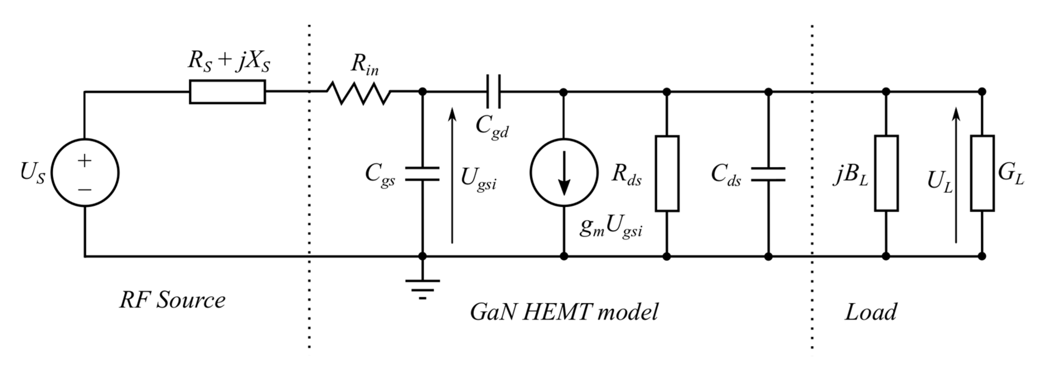
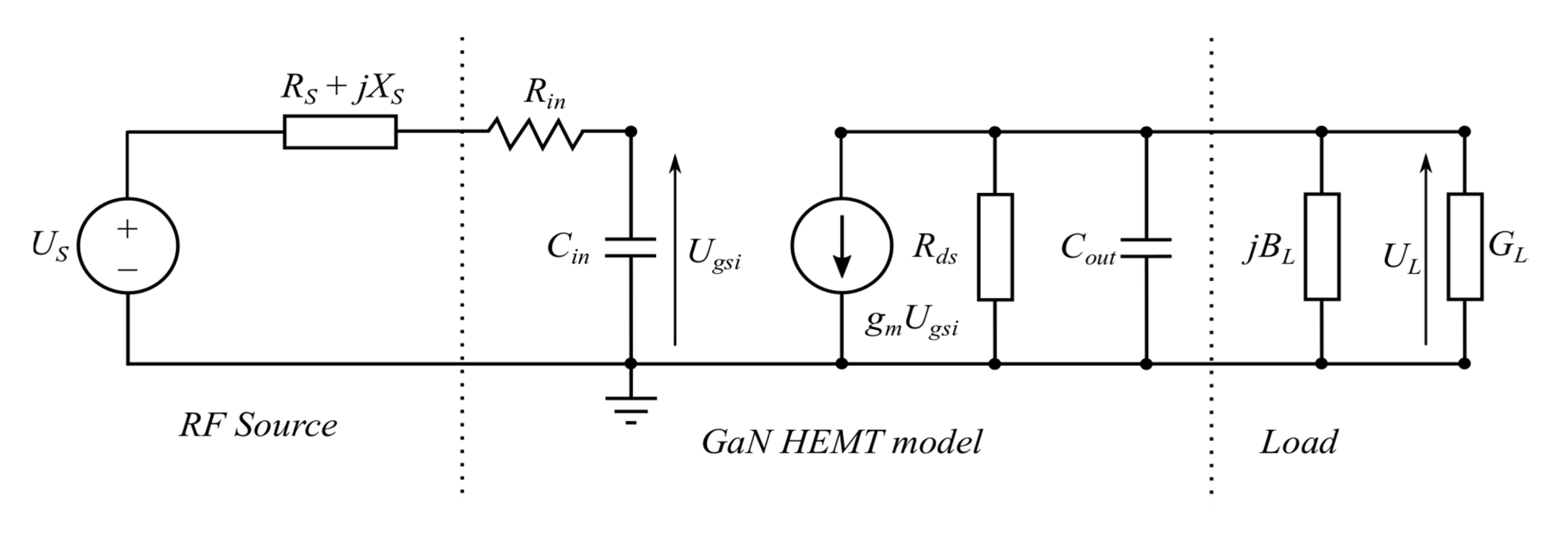
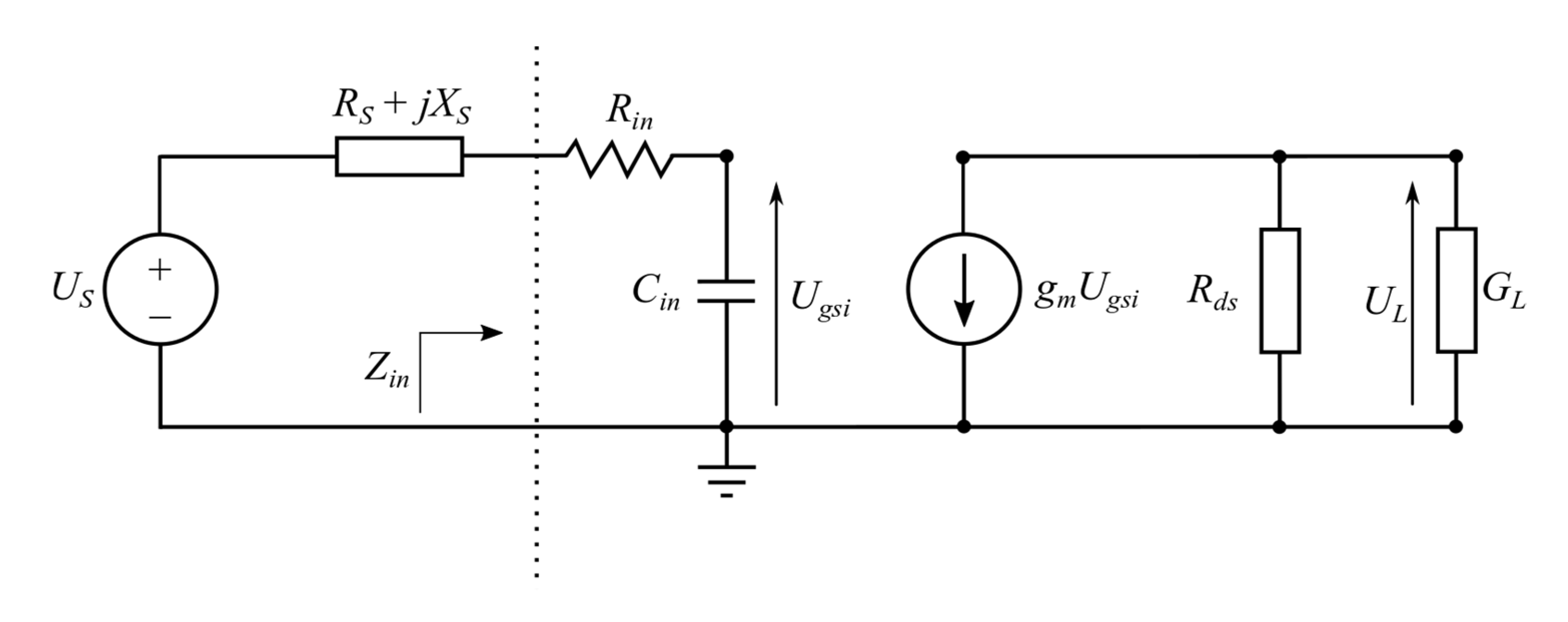
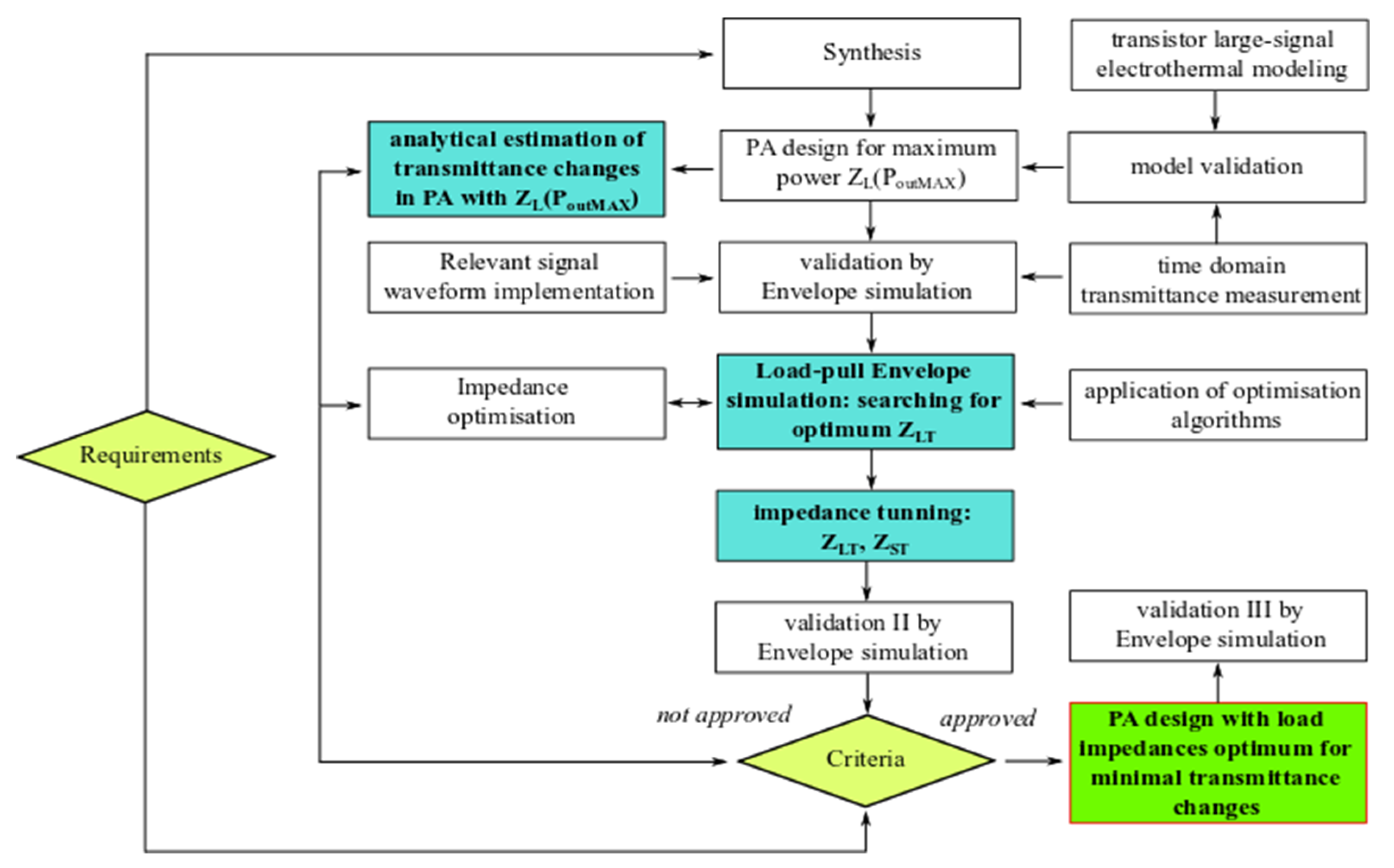
2. Power Amplifier Analysis
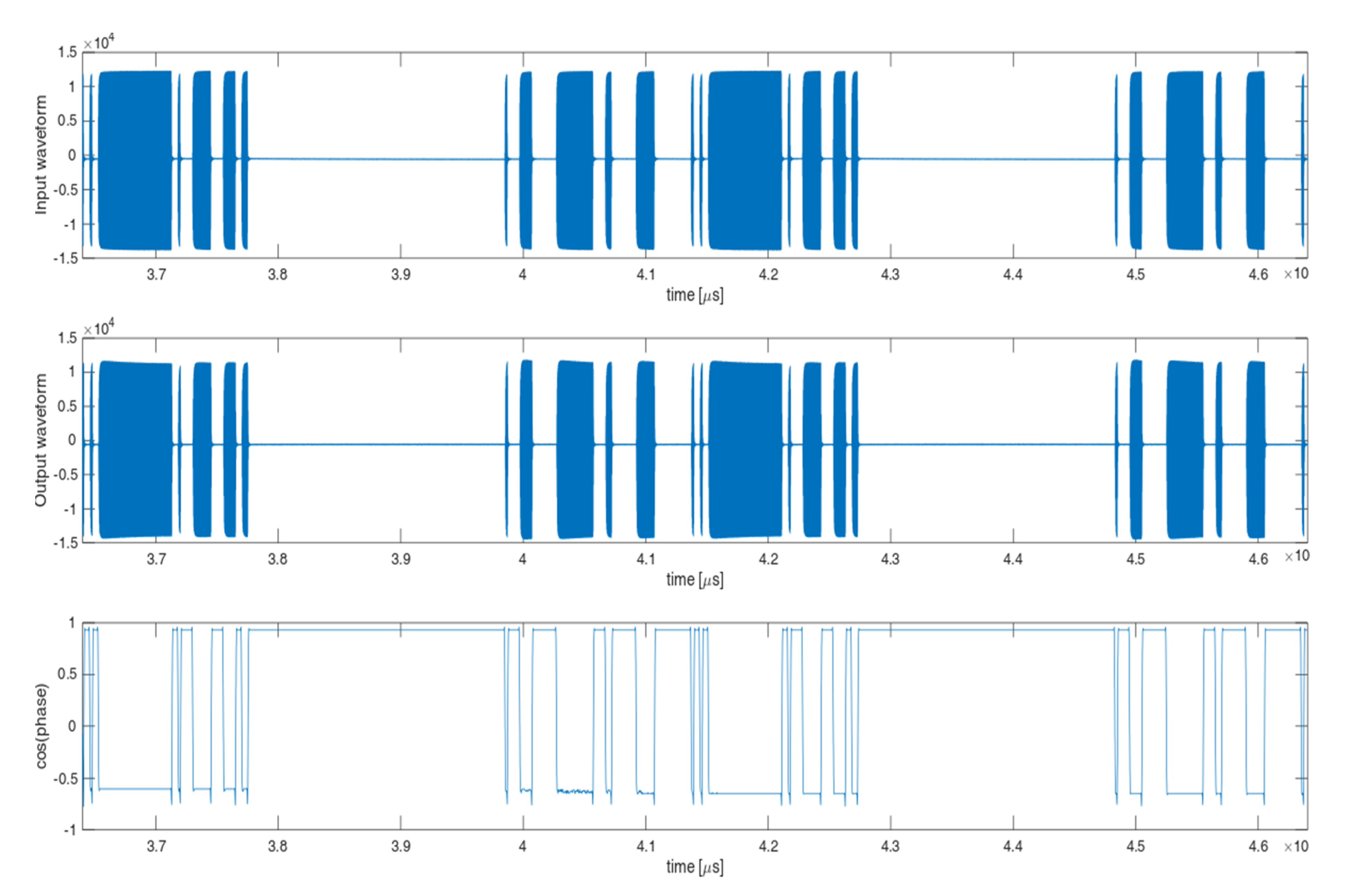
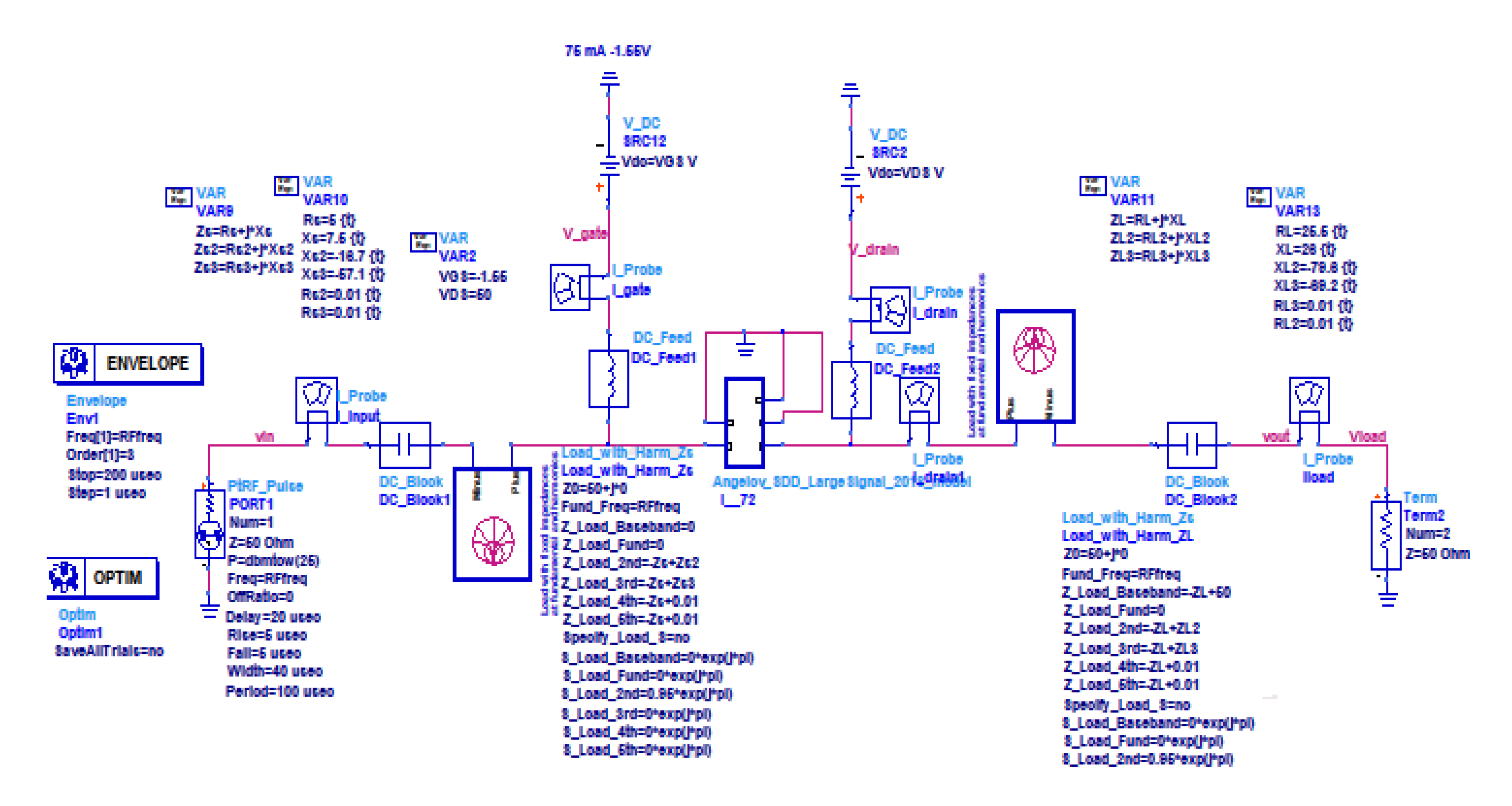
3. Measurement Setup and Amplifier Modelling
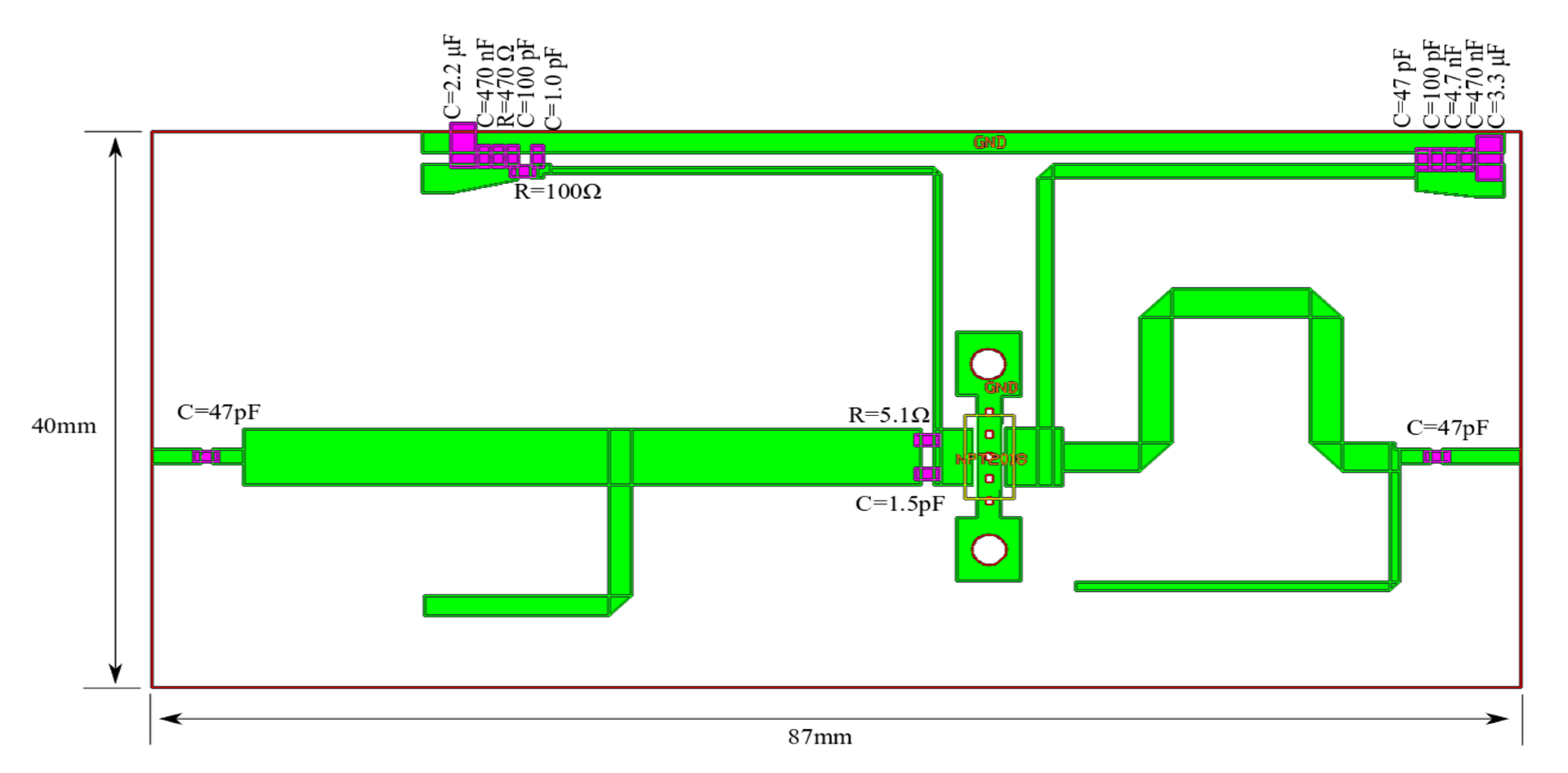
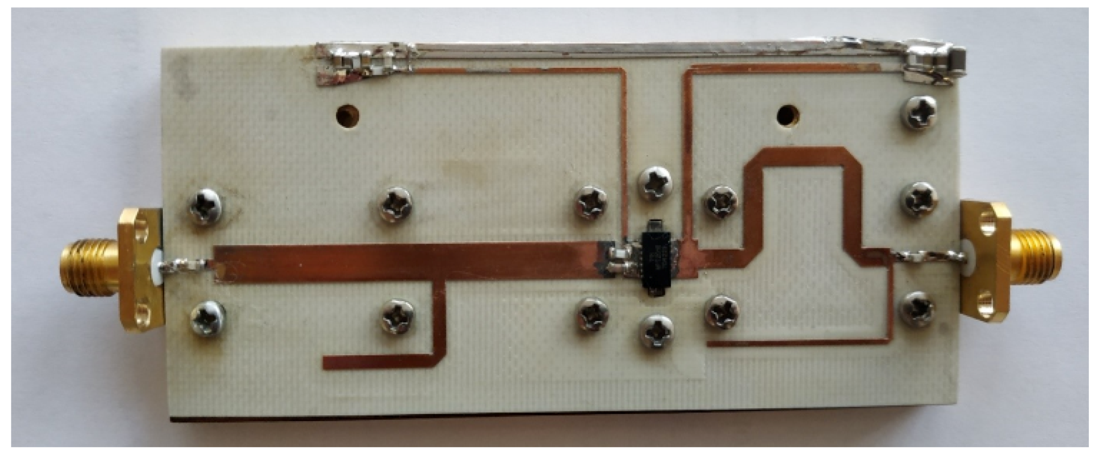
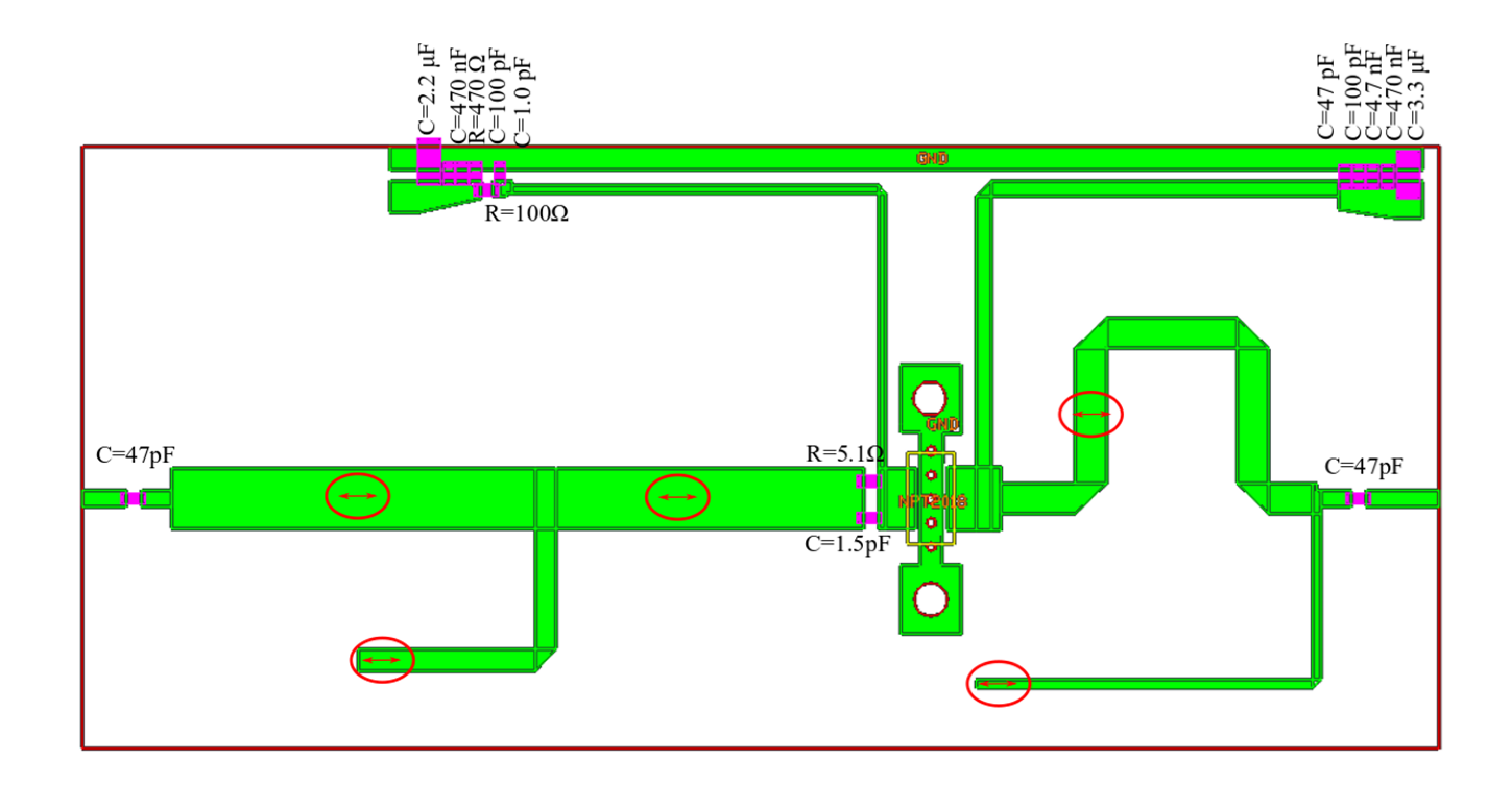
4. Test Amplifier
5. Conclusions
Author Contributions
Funding
Conflicts of Interest
References
- Walker, J.L.B. Handbook of RF and Microwave Power Amplifiers; Cambridge University Press: Cambridge, UK, 2012. [Google Scholar]
- Kuchta, D.; Wojtasiak, W. GaN HEMT Power Amplifer for Radar Waveforms. Proc. SPIE Radioelectron. Syst. 2018, 10715, 1–6. [Google Scholar]
- Asbeck, P.M. Will Doherty Continue to Rule for 5G? IEEE MTT-S International Microwave Symposium (IMS): San Francisco, CA, USA, 2016; pp. 1–4. [Google Scholar]
- Hueber, G.; Niknejad, A.M. Millimeter-Wave Circuits for 5G and Radar; Hueber, G., Niknejad, A.M., Eds.; Cambridge University Press: Cambridge, UK, 2019. [Google Scholar]
- Shafi, M.; Molisch, A.F.; Smith, P.J.; Haustein, T.; Zhu, P.; De Silva, P.; Tufvesson, F.; Benjebbour, A.; Wunder, G. 5G: A tutorial overview of standards, trials, challenges, deployment, and practice. IEEE J. Sel. Areas Commun. 2017, 35, 1201–1221. [Google Scholar] [CrossRef]
- Katz, A.; Wood, J.; Chokola, D. The evolution of PA linearization: From classic feedforward and feedback through analog and digital predistortion. IEEE Microw. Mag. 2016, 2, 32–40. [Google Scholar] [CrossRef]
- Pelaz, J.; Collantes, J.-M.; Otegi, N.; Anakabe, A.; Collins, G. Experimental Control and Design of Low-Frequency Bias Networks for Dynamically Biased Amplififiers. IEEE Trans. Microw. Theory Tech. 2015, 63, 1923–1936. [Google Scholar] [CrossRef]
- Onoe, S. Evolution of 5G mobile technology toward 1 2020 and beyond. In Proceedings of the 2016 IEEE International Solid-State Circuits Conference (ISSCC), San Francisco, CA, USA, 31 January–4 Feberuary 2016. [Google Scholar]
- Lien, S.-Y.; Shieh, S.-L.; Huang, Y.; Su, B.; Hsu, Y.-L.; Wei, H.-Y. 5G new radio: Waveform, frame structure, multiple access, and initial access. IEEE Commun. Mag. 2017, 55, 64–71. [Google Scholar] [CrossRef]
- Kim, B.; Kim, J.; Kim, D.; Son, J.; Cho, Y.; Kim, J.; Park, B. Push the envelope: Design concepts for envelope-tracking power amplifiers. IEEE Microw. Mag. 2013, 14, 68–81. [Google Scholar] [CrossRef]
- Uysal, F.; Yeary, M.; Goodman, N.; Rincon, R.F.; Osmanoglu, B. Waveform design for wideband beampattern and beamforming. In Proceedings of the 2015 IEEE Radar Conference, Arlington, VA, USA, 10–15 May 2015; pp. 1062–1066. [Google Scholar]
- Roh, W.; Seol, J.-Y.; Park, J.; Lee, B.; Lee, J.; Kim, Y.; Cho, J.; Cheun, K.; Aryanfar, F. Millimeter-wave beamforming as an enabling technology for 5G cellular communications: Theoretical feasibility and prototype results. IEEE Commun. Mag. 2014, 52, 106–113. [Google Scholar] [CrossRef]
- Vook, F.W.; Ghosh, A.; Thomas, T.A. MIMO and beamforming solutions for 5G technology. In Proceedings of the 2014 IEEE MTT-S International Microwave Symposium (IMS2014), Tampa, FL, USA, 1–6 June 2014; pp. 1–4. [Google Scholar]
- Dunn, Z.; Yeary, M.; Fulton, C. Frequency-dependent power amplifier modeling and correction for distortion in wideband radar transmissions. In Proceedings of the 2014 IEEE 57th International Midwest Symposium on Circuits and Systems (MWSCAS), College Station, TX, USA, 3–6 August 2014; pp. 61–64. [Google Scholar]
- Fellows, M.; Baylis, C.; Martin, J.; Cohen, L.; Marks, R.J. Direct algorithm for the Pareto load-pull optimization of power-added efficiency and adjacent channel power ratio. IET Radar Sonar Navig. 2014, 8, 1280–1287. [Google Scholar] [CrossRef]
- Baylis, C.; Fellows, M.; Barkate, J.; Tsatsoulas, A.; Rezayat, S.; Lamers, L.; Marks, R.J.; Cohen, L. Circuit optimization algorithms for real-time spectrum sharing between radar and communications. In Proceedings of the 2016 IEEE Radar Conference (RadarConf), Philadelphia, PA, USA, 2–6 May 2016; pp. 1–4. [Google Scholar]
- Chireix, H. High power outphasing modulation. Proc. Inst. Radio Eng. 1935, 23, 1370–1392. [Google Scholar] [CrossRef]
- Wood, J. Behavioral Modeling and Linearization of RF Power Amplifiers; Artech House: Norwood, MA, USA, 2014. [Google Scholar]
- Gryglewski, D.; Wojtasiak, W. Temperature-Dependent Modeling of High-Power MESFET Using Thermal FDTD Method. In Proceedings of the IEEE MTT-S International Microwave Symposium Digest 2001, Phoenix, AZ, USA, 20–26 May 2001; pp. 411–414. [Google Scholar]
- Remsburg, R. Thermal Design of Electronic Equipment; CRC Press: Boca Raton, FL, USA, 2001. [Google Scholar]
- Golio, J.M.; Golio, M. RF and Microwave Passive and Active Technologies. In RF and Microwave Handbook, 2nd ed.; CRC Press: Boca Raton, FL, USA, 2007. [Google Scholar]
- Komiak, J.J. GaN HEMT: Dominant Force in High-Frequency Solid-State Power Amplifiers. IEEE Microw. Mag. 2015, 16, 97–105. [Google Scholar] [CrossRef]
- Miller, J.M. Dependence of the input impedance of a three-electrode vacuum tube upon the load in the plate circuit. Sci. Pap. Bur. Stand. 1920, 15, 367–385. [Google Scholar] [CrossRef]
- Steve, C. Cripps Advanced Techniques in RF Power Amplifier Design; Artech House: Norwood, MA, USA, 2002. [Google Scholar]
- Crupi, G.; Raffo, A.; Avolio, G.; Schreurs, D.M.M.-P.; Vannini, G.; Cassemi, A. Temperature Influence on GaN HEMT Equivalent Circuit. IEEE Microw. Wirel. Compon. Lett. 2016, 26, 813–815. [Google Scholar] [CrossRef]
- Holman, J.P. Heat Transfer, 10th ed.; McGraw-Hill: London, UK, 2010. [Google Scholar]
- Nunes, L.C.; Cabral, P.M.; Pedro, J.C. AM/AM and AM/PM Distortion Generation Mechanisms in Si LDMOS and GaN HEMT Based RF Power Amplifiers. IEEE Trans. Microw. Theory Tech. 2014, 62, 799–809. [Google Scholar] [CrossRef]
- Angelov, I.; Thorsell, M.; Andersson, K.; Rorsman, N.; Kuwata, E.; Ohtsuka, H.; Yamanaka, K. On the Large-Signal Modeling of High Power AlGaN/GaN HEMTs; 2012 IEEE/MTT-S International Microwave Symposium Digest: Montreal, QC, USA, 2012. [Google Scholar]
- Gryglewski, D. The GaN HEMT Thermal Characterization. In Proceedings of the 8th Wide Bandgap Semiconductors and Components Workshop, Harwell, UK, 12–13 September 2016. [Google Scholar]
- Crupia, G.; Avolio, G.; Raffo, A.; Barmuta, P.; Schreurs, D.M.M.-P.; Caddemi, A.; Vannini, G. Investigation on the thermal behavior of microwave GaN HEMTs. Solid-State Electron. 2011, 64, 28–33. [Google Scholar] [CrossRef]
- Ngoya, E.; Larcheveque, R. Envelop transient analysis: A new method for the transient and steady state analysis of microwave communication circuits and systems. In Proceedings of the 1996 IEEE MTT-S International Microwave Symposium Digest, San Francisco, CA, USA, 17–21 June 1996; Volume 3, pp. 1365–1368. [Google Scholar]
- Dunn, Z.; Yeary, M.; Fulton, C.; Goodman, N. Wideband digital predistortion of solid-state radar amplifiers. IEEE Trans. Aerosp. Electron. Syst. 2016, 52, 2452–2466. [Google Scholar] [CrossRef]
- Martin, J.; Moldovan, M.; Baylls, C.; Marks, R.J.; Cohen, L.; de Graaf, J. Radar chirp waveform selection and circuit optimization using ACPR load-pull measurements. In Proceedings of the WAMICON 2012 IEEE Wireless & Microwave Technology Conference, Cocoa Beach, FL, 15–17 April 2012; pp. 1–4. [Google Scholar]
- Apel, T. RF Power Device Characterization Accomplished Through Direct and Indirect Techniques. In Microwave Systems News; EW Communications: Palo Alto, CA, USA, 1984. [Google Scholar]
- Kazimierczuk, M. RF Power Amplifiers, 2nd ed.; John Wiley & Sons: Hoboken, NJ, USA, 2015. [Google Scholar]


| Parameter | NPTB0004A | NPT2018 | NPT2022 |
|---|---|---|---|
| IDA | 0.34 A | 0.6 A | 4 A |
| PSat | 5 W | 16 W | 120 W |
| G′L | 16 mS | 14 ms | 101 ms |
| gm | 670 mS | 584 ms | 3.88 S |
| G′L/gm | 0.024 | 0.025 | 0.026 |
| Cgs | 6.9 pF | 7.8 pF | 42.9 pF |
| Cgd | 0.27 pF | 0.291 pF | 1.66 pF |
| Cds | 0.62 pF | 0.56 pF | 9.9 pF |
| UDS | 28 V | 50 V | 48 V |
| Original | After Optimization | |
|---|---|---|
| 26.4 + 26.6j | 31.8 + 35.7j | |
| 5.6 + 12.0j | 5.2 + 17.5j |
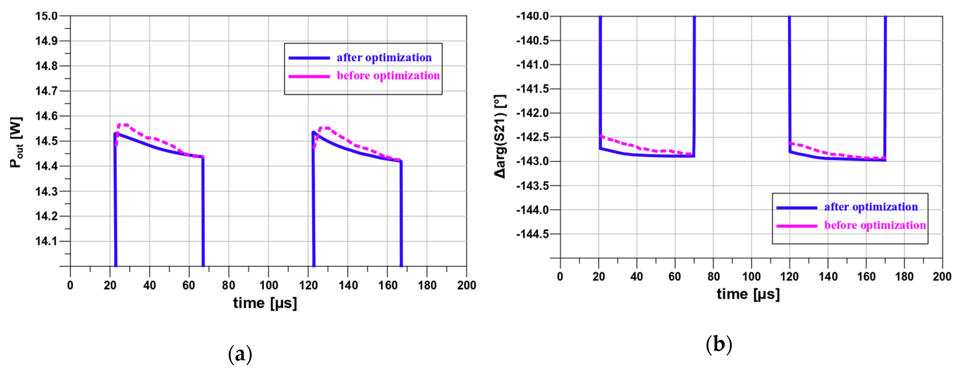
| Before optimization | 0.5 | 0.8 | 17 W | 61 |
| Optimization applied | 0.2 | 0.2 | 14 W | 54 |
© 2020 by the authors. Licensee MDPI, Basel, Switzerland. This article is an open access article distributed under the terms and conditions of the Creative Commons Attribution (CC BY) license (http://creativecommons.org/licenses/by/4.0/).
Share and Cite
Kuchta, D.; Gryglewski, D.; Wojtasiak, W. A GaN HEMT Amplifier Design for Phased Array Radars and 5G New Radios. Micromachines 2020, 11, 398. https://doi.org/10.3390/mi11040398
Kuchta D, Gryglewski D, Wojtasiak W. A GaN HEMT Amplifier Design for Phased Array Radars and 5G New Radios. Micromachines. 2020; 11(4):398. https://doi.org/10.3390/mi11040398
Chicago/Turabian StyleKuchta, Dawid, Daniel Gryglewski, and Wojciech Wojtasiak. 2020. "A GaN HEMT Amplifier Design for Phased Array Radars and 5G New Radios" Micromachines 11, no. 4: 398. https://doi.org/10.3390/mi11040398
APA StyleKuchta, D., Gryglewski, D., & Wojtasiak, W. (2020). A GaN HEMT Amplifier Design for Phased Array Radars and 5G New Radios. Micromachines, 11(4), 398. https://doi.org/10.3390/mi11040398