Low-Power, Multimodal Laser Micromachining of Materials for Applications in sub-5 µm Shadow Masks and sub-10 µm Interdigitated Electrodes (IDEs) Fabrication


Abstract
1. Introduction
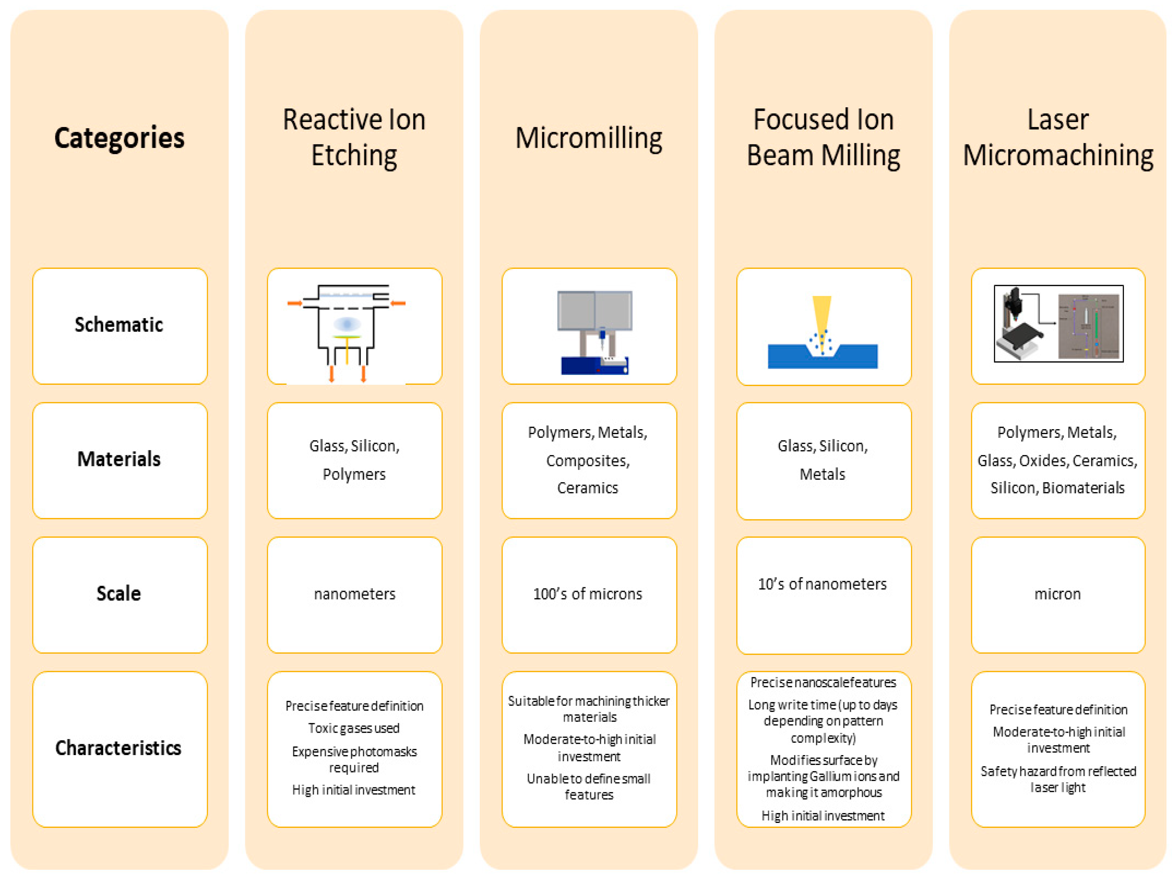
2. Microfabrication Method Overview
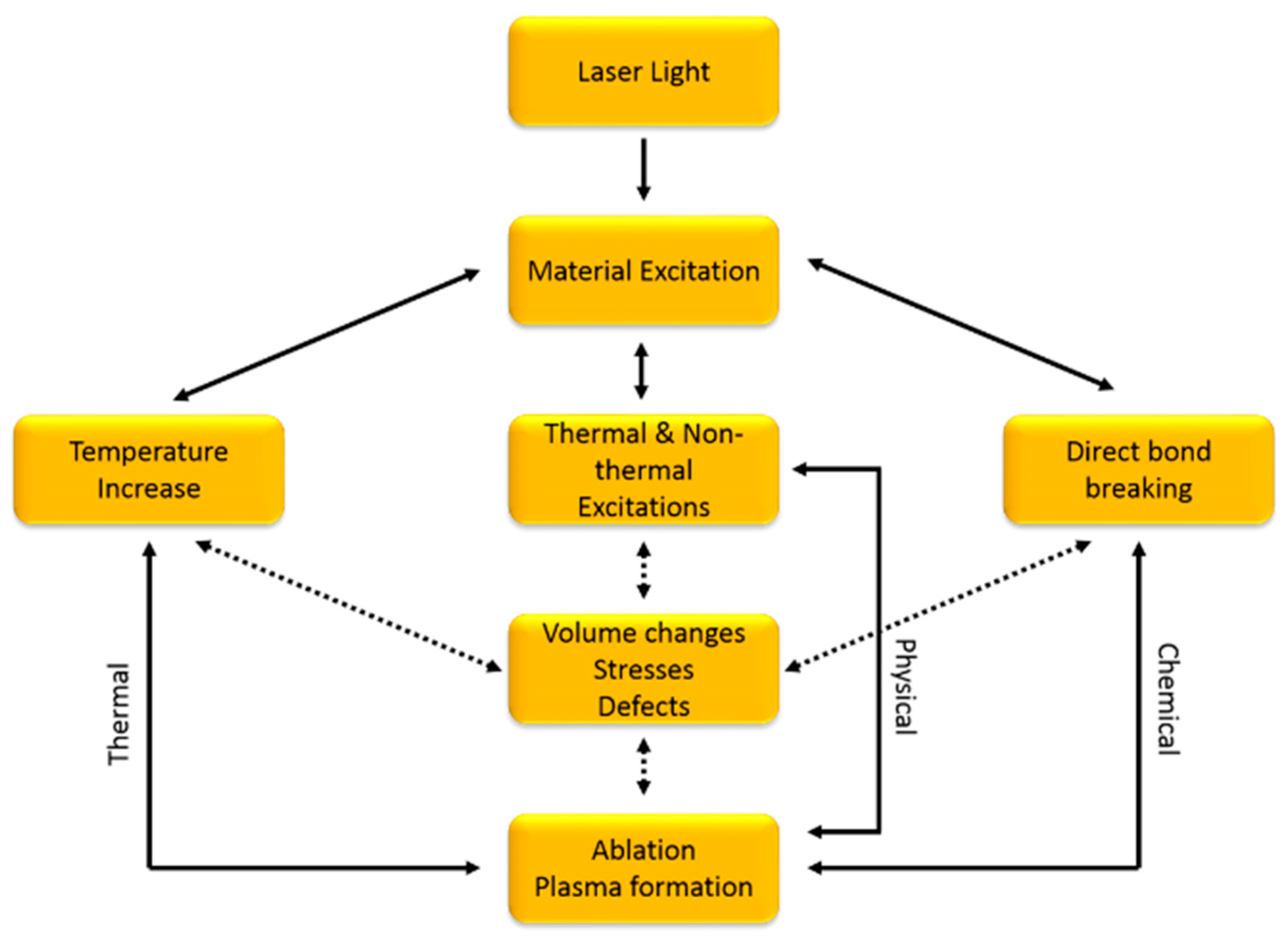
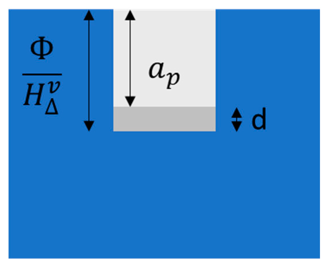
3. Theoretical Background
4. Materials and Methods
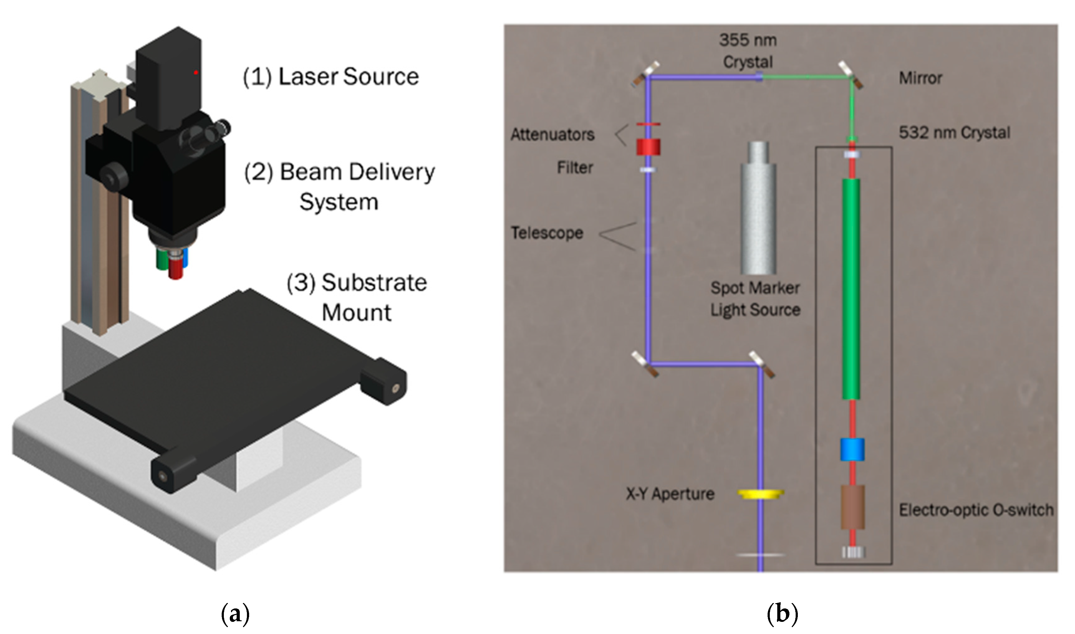
4.1. Multimodal Laser
4.2. Materials Used
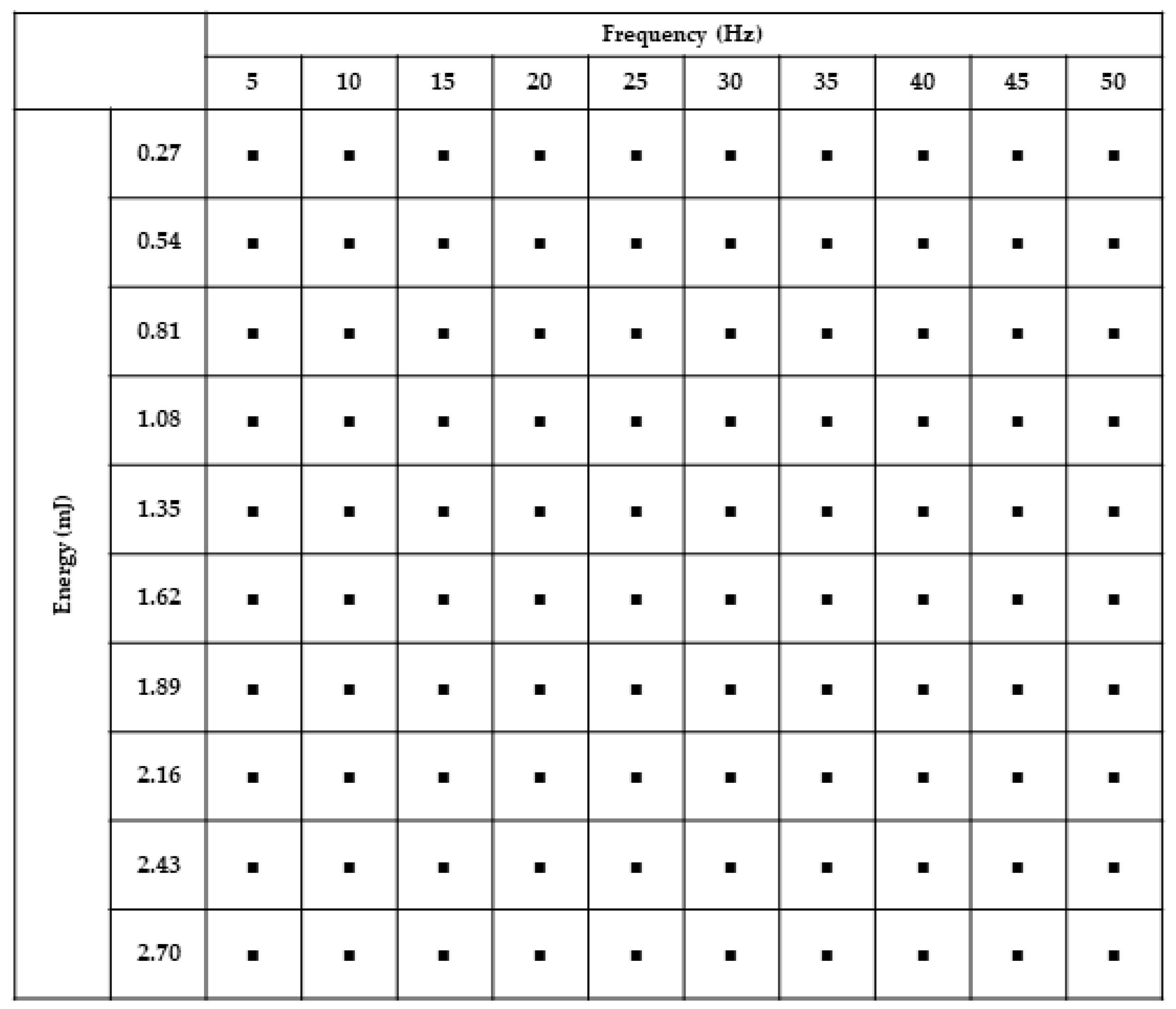
4.3. Laser Characterization
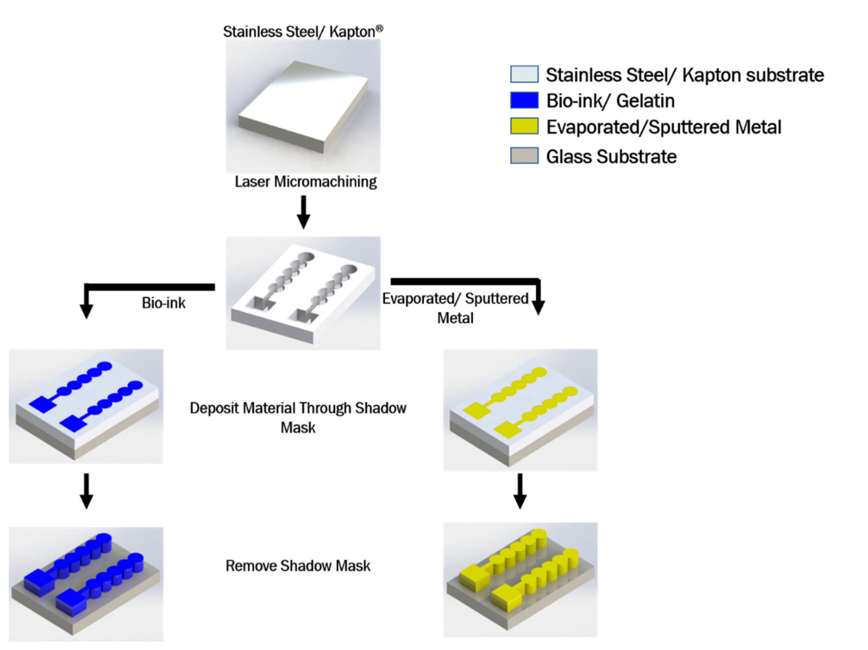
4.4. Shadow Masks
4.5. Patterning of Organic and Inorganic Layers
4.5.1. Metal Patterning
4.5.2. Gelatin Patterning
4.6. Impedance Characterization of Metal Patterns
5. Results and Discussion
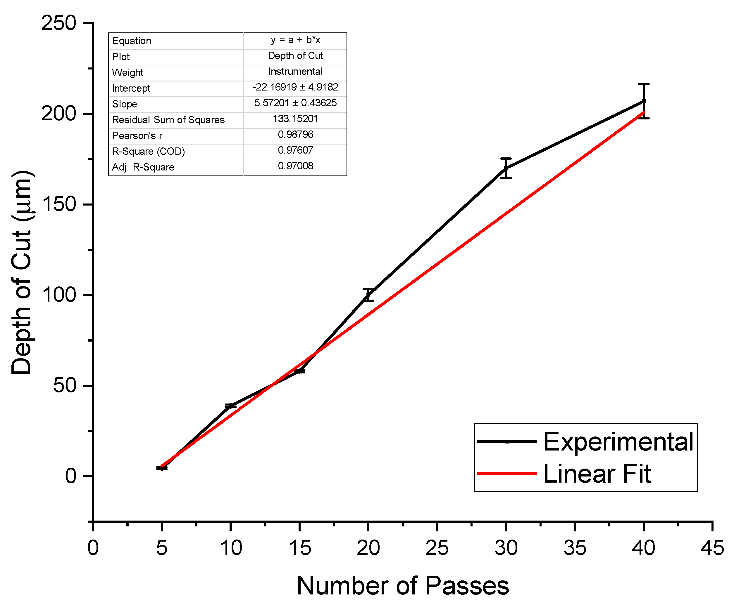
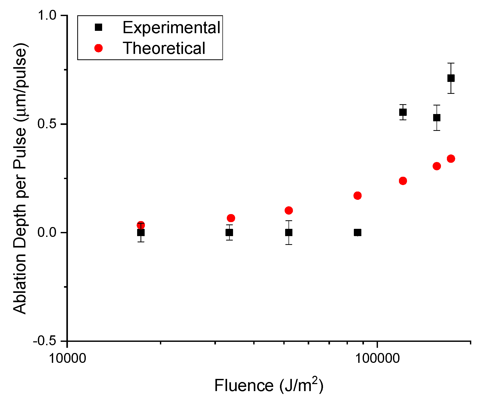
5.1. Laser Characterization
Comparison to Theoretical Values
5.2. Applications
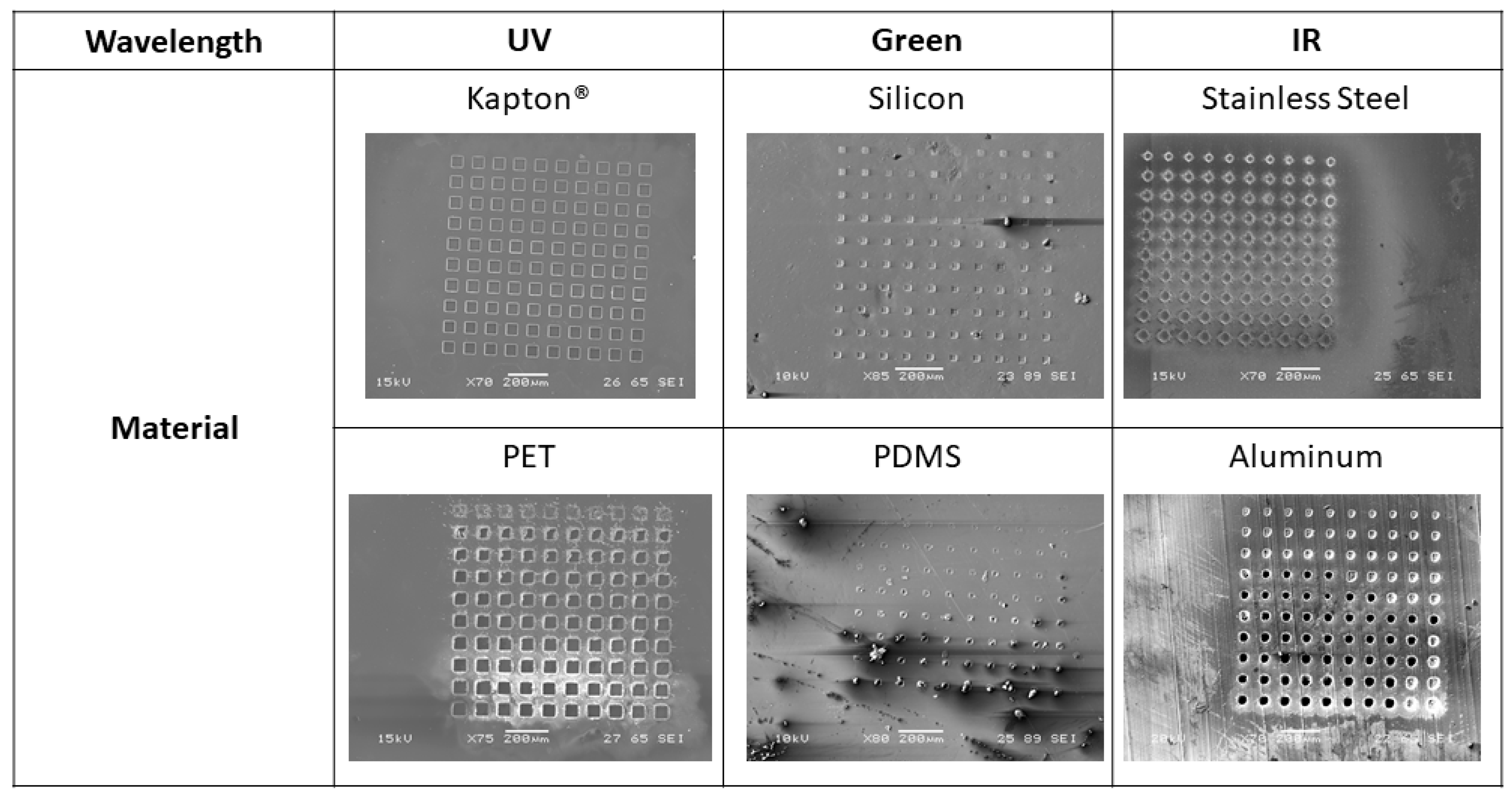
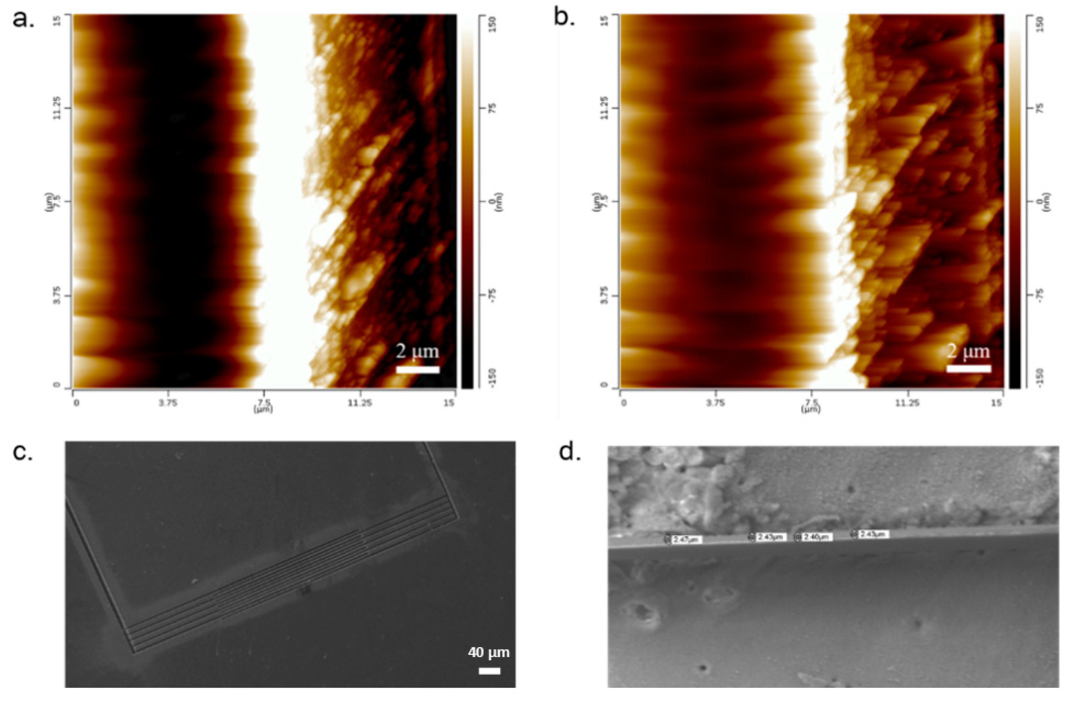
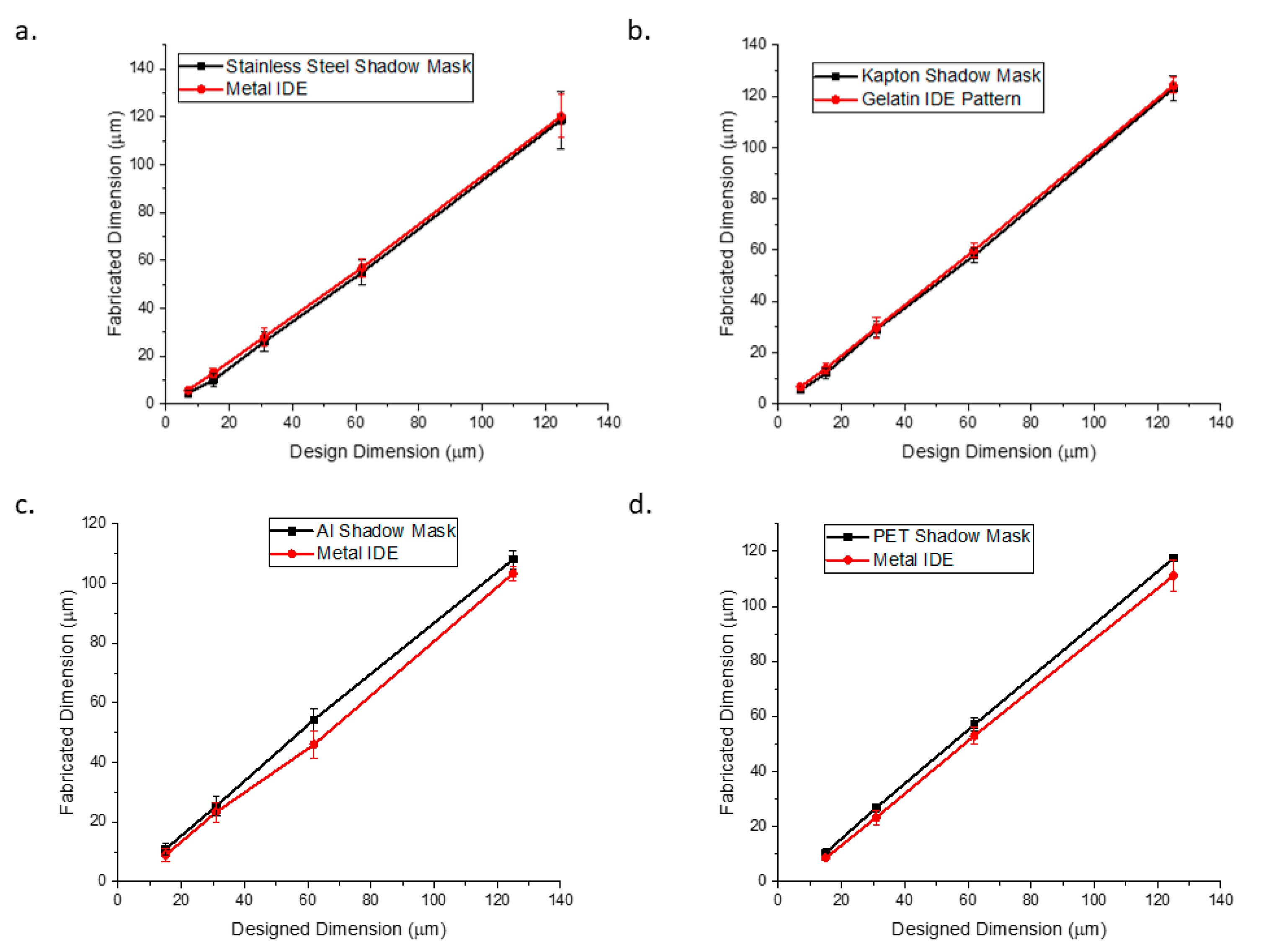
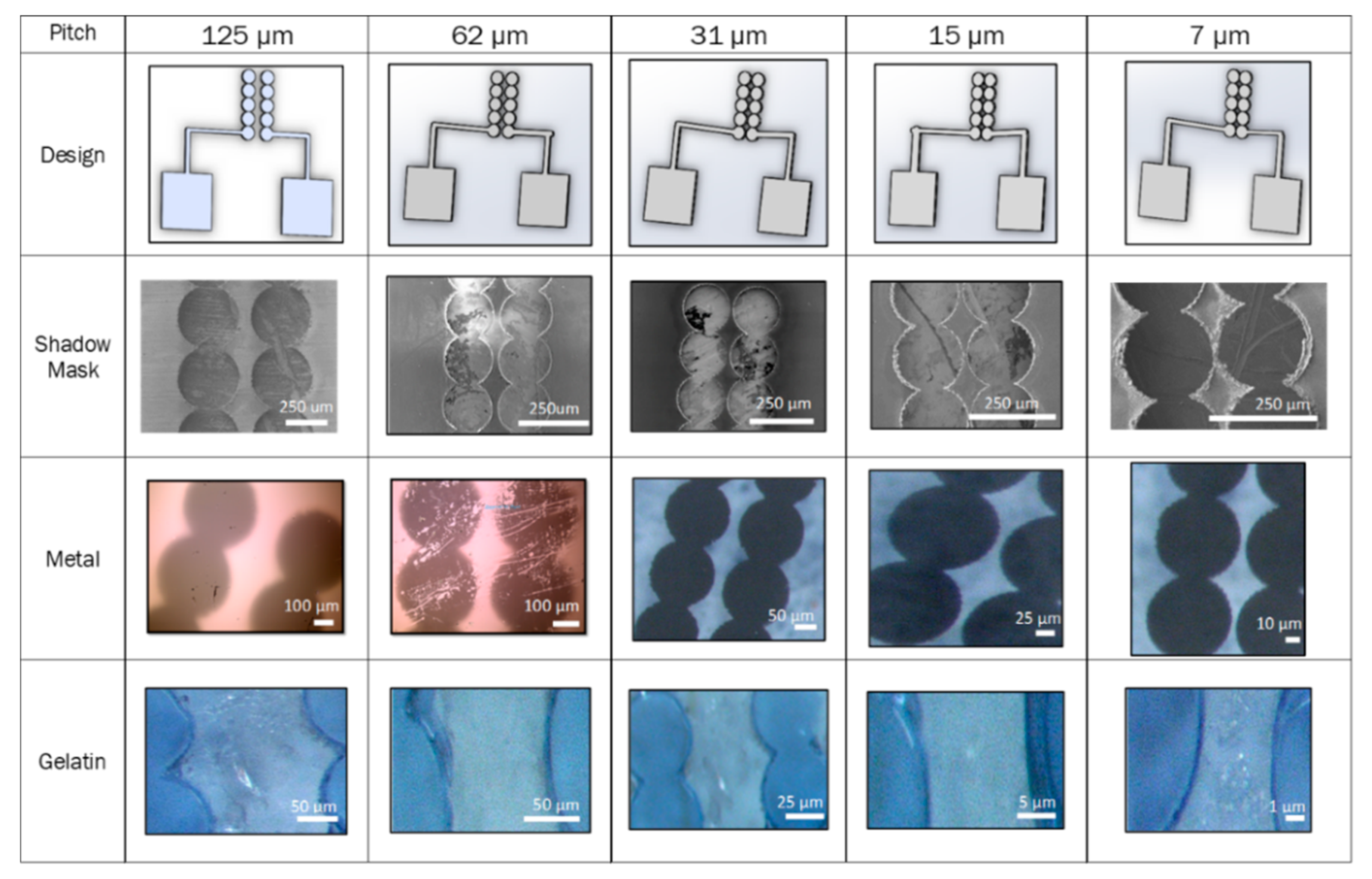
5.2.1. Shadow Masks
5.2.2. Patterning Through Shadow Masks
6. Conclusions
Author Contributions
Funding
Acknowledgments
Conflicts of Interest
References
- Klank, H.; Kutter, J.P.; Geschke, O. CO2-laser micromachining and back-end processing for rapid production of PMMA-based microfluidic systems. Lab Chip 2002, 2, 242–246. [Google Scholar] [CrossRef]
- Anderson, R.R.; Margolis, R.J.; Watenabe, S.; Flotte, T.; Hruza, G.J.; Dover, J.S. Selective photothermolysis of cutaneous pigmentation by q-switched Nd:YAG laser pulses at 1064, 532, and 355 nm. J. Investig. Dermatol. 1989, 93, 28–32. [Google Scholar] [CrossRef] [PubMed]
- Fan, Y.; Li, H.; Yi, Y.; Foulds, I.G. Laser micromachined wax-covered plastic paper as both sputter deposition shadow masks and deep-ultraviolet patterning masks for polymethylmethacrylate-based microfluidic systems. J. Micro/Nanolithography MEMS MOEMS 2013, 12, 049701. [Google Scholar] [CrossRef]
- Hung, Y.H.; Chien, H.L.; Lee, Y.C. Excimer laser three-dimensional micromachining based on image projection and the optical diffraction effect. Appl. Sci. 2018, 8, 1690. [Google Scholar] [CrossRef]
- Arnold, M.S.B.A.C.B. Fundamentals of Laser-Material Interaction and Application to Multiscale Surface Modification. In Laser Precision Microfabrication; Sugioka, M.M.K., Pique, A., Eds.; Springer: Berlin/Heidelberg, Germany, 2010. [Google Scholar]
- Schaeffer, R.D. Fundamentals of Laser Micromachining; CRC Press: Boca Raton, FL, USA, 2012. [Google Scholar]
- Rizvi, N.H.; Apte, P. Developments in laser micro-machining techniques. J. Mater. Process. Technol. 2002, 127, 206–210. [Google Scholar] [CrossRef]
- Arnold, C.B.; Piqué, A. Laser Direct-Write Processing. MRS Bull. 2007, 32, 9–15. [Google Scholar] [CrossRef]
- Miller, P.R.; Aggarwal, R.; Doraiswamy, A.; Lin, Y.J.; Lee, Y.S.; Narayan, R.J. Laser micromachining for biomedical applications. JOM 2009, 61, 35–40. [Google Scholar] [CrossRef]
- Schütz, V.; Stute, U.; Horn, A. Thermodynamic investigations on the laser ablation rate of silicon over five fluence decades. Phys. Procedia 2013, 41, 640–649. [Google Scholar] [CrossRef]
- Gower, M.C. Laser micromachining for manufacturing MEMS devices. In Micromachining and Microfabrication; SPIE: Bellingham, WA, USA, 2001; Volume 4559. [Google Scholar]
- Tahir, B.A.; Ahmed, R.; Ashiq, M.G.B.; Ahmed, A.; Saeed, M.A. Cutting of nonmetallic materials using Nd:YAG laser beam. Chin. Phys. B 2012, 21, 044201. [Google Scholar] [CrossRef]
- Petit, D.; Faulkner, C.C.; Johnstone, S.; Wood, D.; Cowburn, R.P. Nanometer scale patterning using focused ion beam milling. Rev. Sci. Instrum. 2005, 76, 026105. [Google Scholar] [CrossRef]
- Guckenberger, D.J.; de Groot, T.E.; Wan, A.M.; Beebe, D.J.; Young, E.W. Micromilling: A method for ultra-rapid prototyping of plastic microfluidic devices. Lab Chip 2015, 15, 2364. [Google Scholar] [CrossRef] [PubMed]
- Jansen, H.; Gardeniers, H.; de Boer, M.; Elwenspoek, M.; Fluitman, J. A survey on the reactive ion etching of silicon in microtechnology. J. Micromech. Microeng. 1995, 6, 14. [Google Scholar] [CrossRef]
- Utke, I.; Hoffmann, P.; Melngailis, J. Gas-assisted focused electron beam and ion beam processing and fabrication. J. Vac. Sci. Technol. B 2008, 26, 1197. [Google Scholar] [CrossRef]
- Karouta, F. A practical approach to reactive ion etching. J. Phys. D Appl. Phys. 2014, 47, 233501. [Google Scholar] [CrossRef]
- Tseng, A.A. Recent developments in micromilling using focused ion beam technology. J. Micromech. Microeng. 2004, 14, R15. [Google Scholar] [CrossRef]
- Peake, G.M.; Zhang, L.; Li, N.Y.; Sarangan, A.M.; Willison, C.G.; Shul, R.J.; Hersee, S.D. A micromachined, shadow-mask technology for the OMVPE fabrication of integrated optical structures. J. Electron. Mater. 2000, 29, 86–90. [Google Scholar] [CrossRef]
- Jamwal, A.; Aggarwal, A.; Gautam, N.; Devarapalli, A. Nishant Gautam, Akhil Devarapalli, Electro-Discharge Machining: Recent Developments and Trends. Int. Res. J. Eng. Technol. 2018, 5, 433–448. [Google Scholar]
- Kumar, S.; Dvivedi, A. On machining of hard and brittle materials using rotary too micro-ultrasonic drilling process. Mater. Manuf. Process. 2019, 34, 736–748. [Google Scholar] [CrossRef]
- Liu, X.; Liang, Z.; Wen, G.; Yuan, X. Waterjet Machining and Research Developments: A Review. Int. J. Adv. Manuf. Technol. 2019, 102, 1257–1335. [Google Scholar] [CrossRef]
- Kumar, A.; Gupta, A.; Kant, R.; Akhtar, S.N.; Tiwari, N.; Ramkumar, J.; Bhattacharya, S. Optimization of laser machining process for the preparation of photomasks and its application to microsystems fabrication. J. Micro/Nanolithography MEMS MOEMS 2013, 12, 041203. [Google Scholar] [CrossRef]
- Heo, J.; Min, H.; Lee, M. Laser micromachining of permalloy for fine metal mask. Int. J. Precis. Eng. Manuf. —Green Technol. 2015, 2, 225–230. [Google Scholar] [CrossRef]
- Lee, J.H.; Yoon, J.W.; Kim, I.G.; Oh, J.S.; Nam, H.J.; Jung, D.Y. Fabrication of polydimethylsiloxane shadow masks for chemical solution deposition of CdS thin-film transistors. Thin Solid Films 2008, 516, 6492–6498. [Google Scholar] [CrossRef]
- Chung, I.Y.; Kim, J.D.; Kang, K.H. Ablation drilling of invar alloy using ultrashort pulsed laser. Int. J. Precis. Eng. Manuf. 2009, 10, 11–16. [Google Scholar] [CrossRef]
- Cheng, J.Y.; Wei, C.W.; Hsu, K.H.; Young, T.H. Direct-write laser micromachining and universal surface modification of PMMA for device development. Sens. Actuators B Chem. 2004, 99, 186–196. [Google Scholar] [CrossRef]
- Nayak, N.C.; Lam, Y.C.; Yue, C.Y.; Sinha, A.T. CO2-laser micromachining of PMMA: The effect of polymer molecular weight. J. Micromech. Microeng. 2008, 18, 095020. [Google Scholar] [CrossRef]
- Yuan, D.; Das, S. Experimental and theoretical analysis of direct-write laser micromachining of polymethyl methacrylate by CO2 laser ablation. J. Appl. Phys. 2007, 101, 024901. [Google Scholar] [CrossRef]
- Knowles, M.R.H.; Rutterford, G.; Karnakis, D.; Ferguson, A. Micro-machining of metals, ceramics and polymers using nanosecond lasers. Int. J. Adv. Manuf. Technol. 2007, 33, 95–102. [Google Scholar] [CrossRef]
- Li, J.; Ananthasuresh, G.K. A quality study on the excimer laser micromachining of electro-thermal-compliant micro devices. J. Micromech. Microeng. 2000, 11, 38–47. [Google Scholar] [CrossRef]
- Ihlemann, J.; Rubahn, K. Excimer laser micro machining: Fabrication and applications of dielectric masks. Appl. Surf. Sci. 2000, 154, 587–592. [Google Scholar] [CrossRef]
- Pfleging, W.; Bernauer, W.; Hanemann, T.; Torge, M. Rapid fabrication of microcomponents—UV-laser assisted prototyping, laser micro-machining of mold inserts and replication via photomolding. Microsyst. Technol. 2002, 9, 67–74. [Google Scholar] [CrossRef]
- Shiu, P.P.; Knopf, G.K.; Ostojic, M.; Nikumb, S. Rapid fabrication of tooling for microfluidic devices via laser micromachining and hot embossing. J. Micromech. Microeng. 2008, 18, 025012. [Google Scholar] [CrossRef]
- Ricciardi, G.; Cantello, M.; Mariotti, F.; Castelli, P.; Giacosa, P. Micromachining with Excimer Laser. CIRP Ann. 1998, 47, 145–148. [Google Scholar] [CrossRef]
- Teixidor, D.; Thepsonthi, T.; Ciurana, J.; Özel, T. Nanosecond pulsed laser micromachining of PMMA-based microfluidic channels. J. Manuf. Process. 2012, 14, 435–442. [Google Scholar] [CrossRef]
- Liu, X.; Du, D.; Mourou, G. Laser ablation and micromachining with ultrashort laser pulses. IEEE J. Quantum Electron. 1997, 33, 1706–1716. [Google Scholar] [CrossRef]
- Oblov, K.; Ivanova, A.; Soloviev, S.; Samotaev, N.; Lipilin, A.; Vasiliev, A.; Sokolov, A. Fabrication of Microhotplates Based on Laser Micromachining of Zirconium Oxide. Phys. Procedia 2015, 72, 485–489. [Google Scholar] [CrossRef][Green Version]
- Moser, R.; Kunzer, M.; Goßler, C.; Köhler, K.; Pletschen, W.; Schwarz, U.T.; Wagner, J.H. Laser processing of gallium nitride-based light-emitting diodes with ultraviolet picosecond laser pulses. Opt. Eng. 2012, 51, 114301. [Google Scholar] [CrossRef]
- Yeh, J.T.C. Laser ablation of polymers. J. Vac. Sci. Technol. A 1986, 4, 653. [Google Scholar] [CrossRef]
- Kancharla, V.V.; Chen, S. Fabrication of Biodegradable Polymeric Micro-devices using Laser Micromachining. Biomed. Microdevices 2002, 4, 105–109. [Google Scholar] [CrossRef]
- Lorazo, P.; Lewis, L.J.; Meunier, M. Thermodynamic pathways to melting, ablation, and solidification in absorbing solids under pulsed laser irradiation. Phys. Rev. B 2006, 73, 134108. [Google Scholar] [CrossRef]
- Luk’Yanchuk, B.; Bityurin, N.; Himmelbauer, M.; Arnold, N. UV-laser ablation of polyimide: From long to ultra-short laser pulses. Nucl. Instrum. Methods Phys. Res. B 1997, 122, 347–355. [Google Scholar] [CrossRef]
- Zhang, Y.; Zhang, D.; Wu, J.; He, Z.; Deng, X. A thermal model for nanosecond pulsed laser ablation of aluminum. AIP Adv. 2017, 7, 075010. [Google Scholar] [CrossRef]
- DeHoff, R. Thermodynamics in Materials Science, 2nd ed.; CRC Press: Boca Raton, FL, USA, 2006. [Google Scholar]
- Taylor, R.E. CINDAS Data Series on Materials Properties: Thermal Expansion of Solid; ASM International: Materials Park, OH, USA, 1998; Volume 1–4. [Google Scholar]
- Wang, Y.; Shen, N.; Befekadu, G.K.; Pasiliao, C.L. Modeling pulsed laser ablation of aluminum with finite element analysis considering material moving front. Int. J. Heat Mass Transf. 2017, 113, 1246–1253. [Google Scholar] [CrossRef]
- Cheng, J.; Liu, C.S.; Shang, S.; Liu, D.; Perrie, W.; Dearden, G.; Watkins, K. A review of ultrafast laser materials micromachining. Opt. Laser Technol. 2013, 46, 88–102. [Google Scholar] [CrossRef]
- Huang, H.; Guo, Z. Ultra-short pulsed laser PDMS thin-layer separation and micro-fabrication. J. Micromech. Microeng. 2009, 19, 055007. [Google Scholar] [CrossRef]
- Wang, H.; Wu, X.; Dong, P.; Wang, C.; Wang, J.; Liu, Y.; Chen, J. Electrochemical Biosensor Based on Interdigitated Electrodes for Determination of Thyroid Stimulating Hormone. Int. J. Electroch. Sci. 2014, 9, 12–21. [Google Scholar]
- Hart, C.; Kundu, A.; Kumar, K.; Varma, S.J.; Thomas, J.; Rajaraman, S. Rapid nanofabrication of nanostructured interdigitated electrodes (nIDEs) for long-term in vitro analysis of human induced pluripotent stem cell differentiated cardiomyocytes. Biosensors 2018, 8, 88. [Google Scholar] [CrossRef]
- Alexander, F.; Price, D.T.; Bhansali, S. Optimization of interdigitated electrode (IDE) arrays for impedance based evaluation of Hs 578T cancer cells. J. Phys. Conf. Ser. 2010, 224, 012134. [Google Scholar] [CrossRef]


| Material | Thickness (µm) | Maximum Theoretical Ablation Depth Per Pulse (µm/pulse) | Experimental Ablation Depth per Pulse (µm/pulse) | Ablated Through After 10 Pulses? |
|---|---|---|---|---|
| Kapton | 12.5 | 2.65 | 1.25 * | Yes |
| Stainless Steel | 12.5 | 3.18 | 1.25 * | Yes |
| PET (polyethylene terephthalate) | 25 | 15.6 | 2.5 * | Yes |
| Aluminum | 16.3 | 16.3 | 1.63 * | Yes |
| Silicon | 500 | 0.34024 | 0.7112 | No |
| PDMS (polydimethylsiloxane) | 100 | 0.25783 | 0.6481 | No |
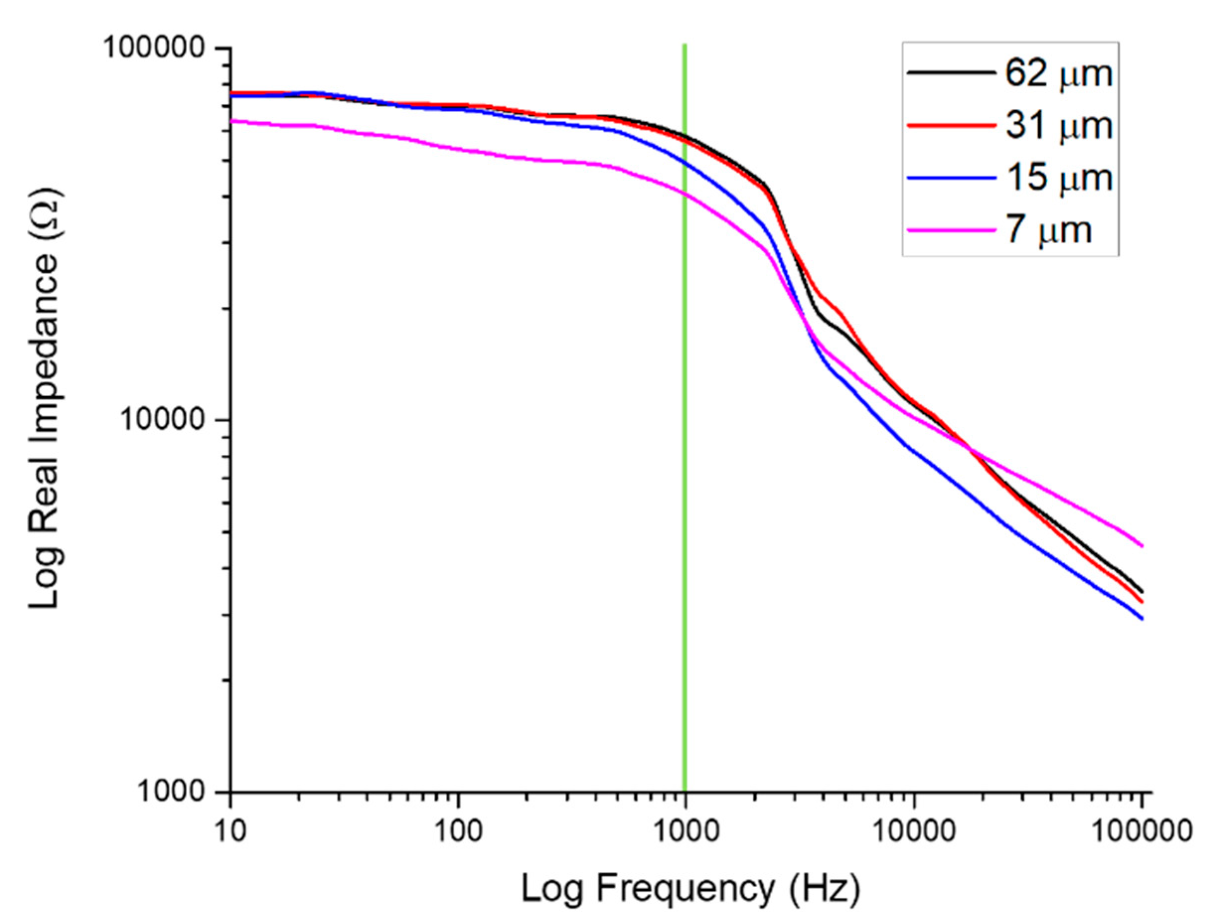
| Impedance at Significant Frequencies | Frequency | Real Impedance (kΩ) | ||||
|---|---|---|---|---|---|---|
| 10 Hz | 100 Hz | 1 kHz | 10 kHz | 100 kHz | ||
| Electrode Gap (μm) | 7 | 63.76 | 53.50 | 40.40 | 10.17 | 4.60 |
| 15 | 74.21 | 68.37 | 48.91 | 8.24 | 2.90 | |
| 32 | 76.06 | 70.29 | 56.06 | 11.19 | 3.26 | |
| 62 | 74.77 | 70.05 | 57.74 | 10.99 | 3.46 | |
| Resistive | Capacitive | Capacitive | Resistive | Resistive | ||
© 2020 by the authors. Licensee MDPI, Basel, Switzerland. This article is an open access article distributed under the terms and conditions of the Creative Commons Attribution (CC BY) license (http://creativecommons.org/licenses/by/4.0/).
Share and Cite
Hart, C.; Rajaraman, S. Low-Power, Multimodal Laser Micromachining of Materials for Applications in sub-5 µm Shadow Masks and sub-10 µm Interdigitated Electrodes (IDEs) Fabrication. Micromachines 2020, 11, 178. https://doi.org/10.3390/mi11020178
Hart C, Rajaraman S. Low-Power, Multimodal Laser Micromachining of Materials for Applications in sub-5 µm Shadow Masks and sub-10 µm Interdigitated Electrodes (IDEs) Fabrication. Micromachines. 2020; 11(2):178. https://doi.org/10.3390/mi11020178
Chicago/Turabian StyleHart, Cacie, and Swaminathan Rajaraman. 2020. "Low-Power, Multimodal Laser Micromachining of Materials for Applications in sub-5 µm Shadow Masks and sub-10 µm Interdigitated Electrodes (IDEs) Fabrication" Micromachines 11, no. 2: 178. https://doi.org/10.3390/mi11020178
APA StyleHart, C., & Rajaraman, S. (2020). Low-Power, Multimodal Laser Micromachining of Materials for Applications in sub-5 µm Shadow Masks and sub-10 µm Interdigitated Electrodes (IDEs) Fabrication. Micromachines, 11(2), 178. https://doi.org/10.3390/mi11020178