Abstract
In this work, Gallium Nitride (GaN)-based p-i-n diodes were designed using a computer aided design (TCAD) simulator for realizing a betavoltaic (BV) cell with a high output power density (Pout). The short-circuit current density (JSC) and open-circuit voltage (VOC) of the 17 keV electron-beam (e-beam)-irradiated diode were evaluated with the variations of design parameters, such as the height and doping concentration of the intrinsic GaN region (Hi-GaN and Di-GaN), which influenced the depletion width in the i-GaN region. A high Hi-GaN and a low Di-GaN improved the Pout because of the enhancement of absorption and conversion efficiency. The device with the Hi-GaN of 700 nm and Di-GaN of 1 × 1016 cm−3 exhibited the highest Pout. In addition, the effects of native defects in the GaN material on the performances were investigated. While the reverse current characteristics were mainly unaffected by donor-like trap states like N vacancies, the Ga vacancies-induced acceptor-like traps significantly decreased the JSC and VOC due to an increase in recombination rate. As a result, the device with a high acceptor-like trap density dramatically degenerated the Pout. Therefore, growth of the high quality i-GaN with low acceptor-like traps is important for an enhanced Pout in BV cell.
1. Introduction
Betavoltaic (BV) cells using a radioisotope have been developed for micro-battery applications, such as a power source of bio-medical implants and extreme environmental sensors [1,2,3], because of their long lifetime and micro-size. 63Ni radioisotope–based BV cells can be used for a long period due to a half-life of about 100 years. The BV cells based on various semiconductors such as Si [4,5], GaAs [6], SiC [7,8,9], GaN [10,11,12,13,14], and GaP [15] have been studied for high power conversion efficiency. Among the semiconductors, it is known that GaN-based BV cells can theoretically obtain superior conversion efficiency because of a wider energy bandgap. Moreover, GaN-based BV cells are more suitable for BV applications with long-term stability because GaN material has exhibited a strong radiation hardness [16,17], which can reduce the effects of radiation damage on device performances [18]. The p-i-n junction [10,11,12] and Schottky barrier diode [13,14] have been used to realize GaN-based BV cells. The p-i-n junction diode can obtain a wider depletion width, which improves the collection efficiency. However, the efficiency of the fabricated device exhibited a lower power conversion efficiency than the theoretical efficiency. Recent studies on BV cells aimed at enhancing the conversion efficiency. Many researchers have made progress in the optimization design of diode structures using a theoretical calculation model [19,20]. However, the design considerations of the GaN-based BV cells still have to be addressed due to the inherent properties of GaN material, including the various native trap states that occur during growth. The short-circuit current density (JSC) and open-circuit voltage (VOC) associated with the output power density of the diode are significantly affected by the native defects that influence recombination.
In this work, we optimized the GaN-based p-i-n diode to achieve a BV cell with high output power density using the following design parameters: heights of p-type GaN and intrinsic GaN (Hp-GaN and Hi-GaN) and a doping concentration of i-GaN (Di-GaN). The physical phenomenon and performance were analyzed using a three-dimensional (3-D) technology computer-aided design (TCAD) simulator with physical models including e-beam irradiation and trap-assisted recombination models. The effects of native defects on JSC, VOC, and Pout of the e-beam-irradiated devices were also investigated.
2. Device Structure and Simulation Method
Figure 1 shows the 3-D schematic of the GaN-based p-i-n diode for BV cells. The p-i-n diode structure is the conventional diode structure, which consisted of an intrinsic GaN (i-GaN) region between p-type GaN (p-GaN) and n-type GaN (n-GaN) regions to obtain a wide width in the depletion region. The Di-GaN determines the depletion width, which affects the conversion efficiency for BV cells. Here, i-GaN denotes undoped GaN, which is almost an n-type due to the residual donor [21]. The background impurity concentration in undoped GaN grown by metal-organic chemical-vapor deposition (MOCVD) is typically in the range of 1015 to 1017 cm−3, depending on the condition of the reactor [22]. Furthermore, it is difficult to grow undoped GaN with simultaneous low doping concentration and high quality [23]. Thus, the Di-GaN was varied in the range of 5 × 1015 cm−3 to 5 × 1016 cm−3 for optimizing the Di-GaN. In order to reduce the resistance of the n-GaN and p-GaN layers, doping concentrations of the n-GaN and p-GaN (Dn-GaN and Dp-GaN) were designed as 5 × 1018 cm−3 and 5 × 1017 cm−3, respectively. We also changed the Hp-GaN and Hi-GaN to achieve high performance. The variation ranges of Hp-GaN and Hi-GaN were 60–200 nm and 500–900 nm, respectively. The ranges of Hp-GaN and Hi-GaN values were determined by considering the penetration depth of 17 keV electrons at about 1 μm [24]. The energy of the e-beam is the average energy of 63Ni [25,26]. The contact resistance for p-GaN and n-GaN in the devices was 1 × 10⁻⁴ Ω·cm2 [27,28].
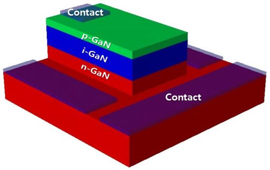
Figure 1.
3-D schematic of the p-i-n diode structure for betavoltaic (BV) cell.
The effects of e-beam irradiation on current characteristics were analyzed using a TCAD simulator [29]. Physical models were applied in the simulation, including Schockley–Read–Hall (SRH) and trap-assisted tunneling (TAT), and a low-field mobility model. The SRH and TAT models were used to reflect the carrier recombination phenomenon [30], which significantly affects the JSC and VOC of the diode. For the effects of native defects in the GaN material [31,32], acceptor and donor-like trap states were added to the simulation. The acceptor-like trap state is formed by Ga vacancies. The donor-like trap states are mainly associated with the N vacancies and nitrogen antisite point defect. When we optimized the structure, we analyzed the performances of the diodes applied by native traps. In addition, the individual impact of trap states on Pout were studied to investigate the dominant traps that degrade the performances.
3. Results and Discussion
Figure 2a shows the effects of e-beam irradiation on the reverse current characteristics of the GaN p-i-n diode. When the diode was irradiated by a 17 keV e-beam, the reverse current density significantly increased. This was because electron-hole pairs (EHPs) were generated by the injected high-energy electrons. The electrons and holes in the depletion region were respectively moved by internal electric field through n-GaN and p-GaN regions and the carriers converted to the electric current. The JSC and a VOC of the irradiated diode were 14.92 μA/cm2 and 2.391 V, respectively. The JSC and VOC were defined as the current density at a voltage of 0 V and the voltage when the current density was 0 A/cm2, respectively.
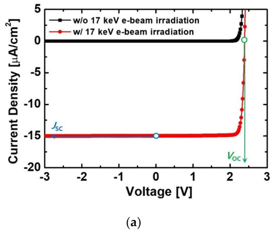
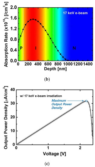
Figure 2.
(a) Effects of e-beam irradiation on reverse current characteristics of the diode. (b) Absorption rate vs. penetration depth in the diode for 17 keV e-beam irradiation. (c) The output power density of the e-beam-irradiated diode. Hp-GaN and Hi-GaN in the diode were 100 nm and 600 nm, respectively. Dp-GaN, Di-GaN, and Dn-GaN were 5 × 1017 cm−3, 1 × 1016 cm−3, and 5 × 1018 cm−3, respectively.
As shown in Figure 2b, the 17 keV electrons penetrated up to a depth of about 1 μm and the peak absorption rate was exhibited at a depth of about 300 nm. Because many EHPs generated in the i-GaN region contributed to the conversion efficiency, the Hi-GaN and Di-GaN are important design parameters. A high conversion efficiency increases JSC and VOC, which influences the output power density (Pout). The diode exhibited the maximum Pout (Pout_max) at a voltage of 2.18 V, as shown in Figure 2c.
Figure 3a shows the variations of the reverse current characteristics of the irradiation diodes as a function of Hi-GaN. As the Hi-GaN increased, the reverse current density became higher due to extension of the absorption region. Many EHPs were generated in the extended absorption region, which converted the electric current. However, the current density of the diodes with a Hi-GaN above 900 nm was lower than that of the device with a Hi-GaN of 700 nm at a forward voltage above 0 V. This result indicated that excess carriers generated by the e-beam were reduced by the recombination mechanism as they moved through the n-GaN or p-GaN regions. This result affected the VOC and JSC of the diodes. As shown in Figure 3b, the device with a Hi-GaN of 700 nm had the highest VOC. In terms of Pout_max, the device with a Hi-GaN of 700 nm exhibited the highest Pout_max because the device was less affected by the recombination phenomenon, as shown in Figure 3c.
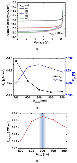
Figure 3.
(a) Reverse current characteristics of the irradiated diodes with different Hi-GaN values. (b) Variations of JSC, VOC and (c) Pout_max as a function of Hi-GaN. The Hp-GaN was fixed as 100 nm. The Dp-GaN, Di-GaN, and Dn-GaN were 5 × 1017 cm−3, 1 × 1016 cm−3, and 5 × 1018 cm−3, respectively.
The variations of JSC, VOC, and Pout_max depending on the Hi-GaN and Hp-GaN are shown in Figure 4. The JSC of the devices increased with a rise in the Hi-GaN regardless of the Hp-GaN because a high Hi-GaN extended the absorption region. When the Hi-GaN above 800 nm increased, the JSC slightly decreased due to the recombination phenomenon. As the Hp-GaN became shorter, the variation of JSC according to the Hi-GaN increased. This result indicated that the absorption rate vs. depth was more affected in the irradiated device with a short Hp-GaN. The device with a Hp-GaN of 60 nm and Hi-GaN of 800 nm was the highest JSC because the JSC was enhanced by an additional absorption near the p-GaN region. In case of the VOC, the device with a Hp-GaN of 100 nm and a Hi-GaN of 700 nm exhibited the highest VOC, as shown in Figure 4b. Because a short Hp-GaN degenerated the carrier transport, the VOC of the devices with a Hp-GaN of 60 nm was a smaller than that of the devices with a Hp-GaN of 100 nm. The device also obtained the highest Pout_max. The Pout_max value was affected by a change of the VOC.
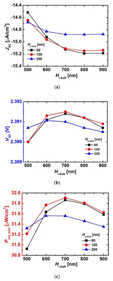
Figure 4.
Variations of (a) JSC, (b) VOC and (c) Pout_max of the irradiated diodes dependent on the Hi-GaN and Hp-GaN. The Dp-GaN, Di-GaN, and Dn-GaN were 5 × 1017 cm−3, 1 × 1016 cm−3, and 5 × 1018 cm−3, respectively.
Figure 5 shows energy band diagrams of the diodes with different values of Di-GaN. As the Di-GaN decreased, the depletion region was extended in the i-GaN region. Because the depletion region was influenced by the Di-GaN, we examined the variations of JSC, VOC and Pout_max depending on the Di-GaN and Hi-GaN. As shown in Figure 6, the diode with a low Di-GaN exhibited an improved JSC because of a wider depletion region in the i-GaN region. The excess carriers could be moved by the built-in electric field. Although the device with a Di-GaN of 1 × 1016 cm−3 exhibited a higher VOC, the diode with a Di-GaN of 5 × 1015 cm−3 obtained a higher Pout_max. This result indicated that reducing the Di-GaN is important to improving transport efficiency. However, in terms of GaN epitaxial technology based on MOCVD method, it was difficult to reduce the Di-GaN below 1 × 1016 cm−3 because residual impurities remained during the growth process. Therefore, we determined that the optimum point for the Di-GaN was 1 × 1016 cm−3. As a result, the diode structure with a Hp-GaN of 100 nm, Hi-GaN of 700 nm, and Di-GaN of 1 × 1016 cm−3 was optimized, and the effects of native trap states on performances of the optimized diode were investigated with variations of trap level and density.
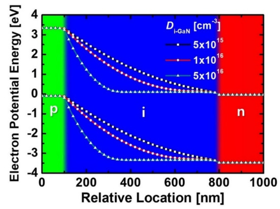
Figure 5.
Energy band diagrams of the diodes with different values of Di-GaN. All the devices were designed with a Hp-GaN of 100 nm and a Hi-GaN of 700 nm. The Dp-GaN and Dn-GaN of the devices were 5 × 1017 cm−3 and 5 × 1018 cm−3, respectively.
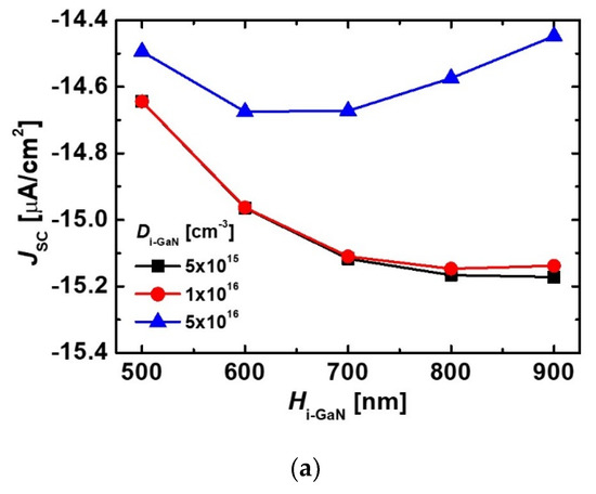
Figure 6.
Variations of (a) JSC, (b) VOC and (c) Pout_max of the e-beam-irradiated diodes depending on Hi-GaN and Di-GaN. All devices were designed with a Hp-GaN of 100 nm and Hi-GaN of 700 nm. The Dp-GaN and Dn-GaN of the devices were 5 × 1017 cm−3 and 5 × 1018 cm−3, respectively.
The energy spectrum of the 63Ni source exhibited a wide range to a 66 keV peak energy [19]. We additionally confirmed the performances of the optimized diode depending on the injected electron energy. The current characteristics of the diodes irradiated by different e-beam energies is shown in Figure 7a. As the energy increased up to 30 keV, the current became higher. This was because many EHPs were generated by a wide distribution of absorption rate as shown in Figure 7b. However, when the electrons with an energy above 40 keV were injected, the current of the irradiated device was lower than that of the device irradiated by the 17 keV e-beam. These results revealed that the variations of the current of the irradiated diodes depending on the energy of the e-beam were large. The probability of beta particles generated from the 63Ni source showed a high distribution below 20 keV [19]. Also, the depletion width formed in the i-GaN region was small at about 600 nm (in case of Di-GaN = 1 × 1016 cm−3), and the diffusion length of GaN can be shortened by native defects. Therefore, in order to achieve a high efficiency BV cell using the 63Ni source, it is necessary to analyze the performances of GaN-based diodes considering the spectrum of the 63Ni source.
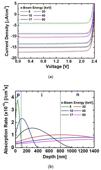
Figure 7.
(a) Current characteristics of the diodes irradiated by different e-beam energies and (b) absorption rate varied by different e-beam energies. All devices were designed with a Hp-GaN of 100 nm and Hi-GaN of 700 nm. The Dp-GaN and Dn-GaN of the devices were 5 × 1017 cm−3 and 5 × 1018 cm−3, respectively.
Figure 8 shows reverse current density and Pout of the irradiated diodes with and without the native trap states including donor and acceptor-like traps. The reverse current density was significantly degenerated by the trap states. This result means that the trap-assisted recombination was caused by the native defects in the GaN material. As a result, the Pout of the device with the trap states was lower than that of the device without the trap states. We confirmed the effects of individual traps on current characteristics of the irradiated devices. As a shown in Figure 9, the impact of acceptor-like trap states was stronger than that of donor-like trap states. This result proved that the acceptor-like trap states represented the dominant factor for the recombination.
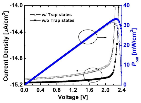
Figure 8.
Current characteristics and Pout of the e-beam-irradiated diodes without and with native trap states. The Hp-GaN and Hi-GaN in the diode were 100 nm and 700 nm, respectively. Dp-GaN, Di-GaN, and Dn-GaN were 5 × 1017 cm−3, 1 × 1016 cm−3, and 5 × 1018 cm−3, respectively.
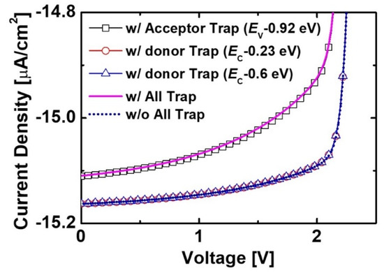
Figure 9.
Effects of trap states on current characteristics of the e-beam-irradiated diodes. The Hp-GaN and Hi-GaN in the diode were 100 nm and 700 nm, respectively. Dp-GaN, Di-GaN, and Dn-GaN were 5 × 1017 cm−3, 1 × 1016 cm−3, and 5 × 1018 cm−3, respectively.
In addition, we investigated the effects of trap density on JSC, VOC, and Pout_max. As the trap density increased, the performances were totally degenerated by the acceptor-like trap state, as shown in Figure 10. The donor-like trap states reduced the JSC less than the acceptor-like trap state. While the donor-like trap states (EC-0.6 eV) slightly decreased the VOC, the shallow donor-like trap states (EC-0.23 eV) increased VOC. As a result, the Pout_max was unaffected by the shallow donor-like trap states (EC-0.23 eV). It is important to reduce the acceptor-like traps to improve the conversion efficiency of the betavoltaic cell.
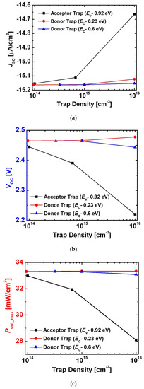
Figure 10.
Effects of each donor and acceptor trap states on (a) JSC, (b) VOC, and (c) Pout_max of the e-beam-irradiated diodes. The Hp-GaN and Hi-GaN in the diode were 100 nm and 700 nm, respectively. Dp-GaN, Di-GaN, and Dn-GaN were 5 × 1017 cm−3, 1 × 1016 cm−3, and 5 × 1018 cm−3, respectively.
4. Conclusions
In this work, we designed a p-i-n diode with a variation of geometric parameters, namely, Hi-GaN, Di-GaN, and Hp-GaN, and analyzed Pout using 17 keV e-beam irradiation. The Hi-GaN and Hp-GaN affected the absorption rate vs. depth. A low Di-GaN produced an increase in depletion width. The optimized structure with a Hi-GaN of 700 nm, Di-GaN of 1 × 1016 cm−3, and Hp-GaN of 100 nm obtained an improved Pout. In addition, the effects of native trap states on reverse current characteristics were investigated with various trap levels and densities. When the acceptor-like trap density increased from 1014 cm−3 to 1016 cm−3, the trap significantly decreased the Pout_max by about 15%. GaN with low acceptor-like traps was needed to enhance the Pout of a BV cell. These results provide design considerations for achieving a high efficiency BV cell.
Author Contributions
Conceptualization, Y.J.Y. and D.S.K.; Investigation, Y.J.Y.; Data analysis, Y.J.Y., J.S.L., I.M.K., J.H.L., and D.S.K.; writing—original draft preparation, Y.J.Y.; writing—review and editing, D.S.K. All authors have read and agreed to the published version of the manuscript.
Funding
This work was supported by the National Research Foundation of Korea (NRF) grant (No. NRF-2018M2A2B3A01072437) funded by the Korea government-MSIT (Ministry of Science and ICT).
Conflicts of Interest
The authors declare no conflict of interest.
References
- Prelas, M.A.; Weaver, C.L.; Watermann, M.L.; Lukosi, E.D.; Schott, R.J.; Wisniewski, D.A. A review of nuclear batteries. Prog. Nucl. Energy 2014, 75, 117–148. [Google Scholar] [CrossRef]
- Spickler, J.W.; Rasor, N.S.; Kezdi, P.; Misra, S.N.; Robins, K.E.; Leboeuf, C. Totally self-contained intracardiac pacemaker. J. Electrocardiol. 1970, 3, 325–331. [Google Scholar] [CrossRef]
- Ko, W.H.; Hynecek, J. Implant evaluation of a nuclear power source-betacel battery. IEEE Trans. Biomed. Eng. 1974, 3, 238–241. [Google Scholar] [CrossRef] [PubMed]
- Rappaport, P. The Electron-Voltaic Effect in p-n Junctions Induced by Beta-Particle Bombardment. Phys. Rev. 1954, 93, 246–247. [Google Scholar] [CrossRef]
- Uhm, Y.R.; Choi, B.G.; Kim, J.B.; Jeong, D.-H.; Son, K.J. Study of a Betavoltaic Battery Using Electroplated Nickel-63 on Nickel Foil as a Power Source. Nucl. Eng. Technol. 2016, 48, 773–777. [Google Scholar] [CrossRef]
- Butera, S.; Lioliou, G.; Barnett, A.M. Temperature effects on gallium arsenide 63Ni betavoltaic cell. Appl. Radiat. Isot. 2017, 125, 42–47. [Google Scholar] [CrossRef]
- Chandrashekhar, M.V.S.; Thomas, C.I.; Li, H.; Spencer, M.G.; Lal, A. Demonstration of a 4H SiC betavoltaic cell. Appl. Phys. Lett. 2006, 88, 033506. [Google Scholar] [CrossRef]
- Thomas, C.; Portnoff, S.; Spencer, M.G. High efficiency 4H-SiC betavoltaic power sources using tritium radioisotopes. Appl. Phys. Lett. 2016, 108, 013505. [Google Scholar] [CrossRef]
- Simulation and Optimization Design of SiC-Based PN Betavoltaic Microbattery Using Tritium Source. Crystals 2020, 10, 105. [CrossRef]
- Munson, C.E.; Arif, M.; Streque, J.; Belahsene, S.; Martinez, A.; Ramdane, A.; Gmili, Y.E.; Salvestrini, J.-P.; Voss, P.L.; Ougazzaden, A. Model of Ni-63 battery with realistic PIN structure. J. Appl. Phys. 2015, 118, 105101. [Google Scholar] [CrossRef]
- Khan, M.R.; Smith, J.R.; Tompkins, R.P.; Kelley, S.; Litz, M.; Russo, J.; Leathersich, J.; Shahedipour-Sandvik, R.; Jones, K.A.; Iliadis, A. Design and characterization of GaN p-i-n diodes for betavoltaic devices. Solid-State Electron. 2017, 136, 24–29. [Google Scholar] [CrossRef]
- Munson, C.E.; Gaimard, Q.; Merghem, K.; Sundaram, S.; Rogers, D.J.; Sanoit, J.; Voss, P.L.; Ramdane, A.; Salvestrini, J.P.; Ougazzaden, A. Modeling, design, fabrication and experimentation of a GaN-based, 63Ni betavoltaic battery. J. Phys. D Appl. Phys. 2018, 51, 035101. [Google Scholar] [CrossRef]
- Lu, M.; Zhang, G.-G.; Fu, K.; Yu, G.-H.; Su, D.; Hu, J.-F. Gallium Nitride Schottky betavoltaic nuclear batteries. Energy Convers. Manag. 2011, 52, 1955–1958. [Google Scholar] [CrossRef]
- San, H.; Yao, S.; Wang, X.; Cheng, Z.; Chen, X. Design and simulation of GaN based Schottky betavoltaic nuclear micro-battery. Appl. Radiat. Isot. 2013, 80, 17–22. [Google Scholar] [CrossRef] [PubMed]
- McNamee, S.; Wagner, D.; Fiordaliso, E.M.; Novog, D.; LaPierre, R.R. GaP nanowire betavoltaic device. Nanotechnology 2019, 30, 075401. [Google Scholar] [CrossRef] [PubMed]
- Ionascut-Nedelcescu, A.; Carlone, C.; Houdayer, A.; von Bardeleben, H.J.; Cantin, J.-L.; Raymond, S. Radiation Hardness of Gallium Nitride. IEEE Trans. Nucl. Sci. 2002, 49, 2733–2738. [Google Scholar] [CrossRef]
- Polyakov, A.Y.; Pearton, S.J.; Frenzer, P.; Ren, F.; Liu, L.; Kim, J. Radiation effects in GaN materials and devices. J. Mater. Chem. C 2013, 1, 877–887. [Google Scholar] [CrossRef]
- Belahsene, S.; Saqri, N.A.A.; Jameel, D.; Mesli, A.; Martinez, A.; Sanoit, J.; Ougazzaden, A.; Salvestrini, J.P.; Ramdane, A.; Henini, M. Analysis of Deep Level Defects in GaN p-i-n Diodes after Beta Particle Irradiation. Electronics 2015, 4, 1090–1100. [Google Scholar] [CrossRef]
- Zheng, R.; Lu, J.; Liu, Y.; Li, X.; Xu, X.; He, R.; Tao, Z.; Gao, Y. Comparative study of GaN betavoltaic bettery based on p-n junction and Schottky barrier diode. Radiat. Phys. Chem. 2020, 168, 108595. [Google Scholar] [CrossRef]
- Bouzid, F.; Pezzimenti, F.; Dehimi, L. Modelling and performance analysis of a GaN-based n/p junction betavoltaic cell. Nucl. Instum. Methods Phys. Res. A 2020, 969, 164103. [Google Scholar] [CrossRef]
- Boguslawski, P.; Briggs, E.L.; Bernholc, J. Native defects in gallium nitride. Phys. Rev. B 1995, 51, 17255–17259. [Google Scholar] [CrossRef] [PubMed]
- Alugubelli, S.R.; Fu, H.; Fu, K.; Liu, H.; Zhao, Y.; Ponce, F.A. Dopant profiling in p-i-n GaN structures using secondary electrons. J. Appl. Phys. 2019, 126, 015704. [Google Scholar] [CrossRef]
- Cheng, Z.J.; San, H.S.; Feng, B.; Liu, B.; Chen, X.Y. High open-circuit voltage betavoltaic cell based on GaN pin homojunction. Electron. Lett. 2011, 47, 720–722. [Google Scholar] [CrossRef]
- Aydin, S.; Kam, E. Investigation of nickel-63 radioisotope-powered GaN betavoltaic nuclear battery. Int. J. Energy Res. 2019, 43, 8725–8738. [Google Scholar] [CrossRef]
- Zuo, G.; Zhou, J.; Ke, G. A Simple theoretical model for 63Ni betavoltaic battery. Appl. Radiat. Isot. 2013, 82, 119–125. [Google Scholar] [CrossRef]
- Belghachi, A.; Bozkurt, K.; Moughli, H.; Ozdemir, O.; Amiri, B.; Talhi, A. A Model for Ni-63 Source for Betavoltaic Application. Acta Phys. Pol. A 2020, 137, 324–331. [Google Scholar] [CrossRef]
- Wang, D.-F.; Shiwei, F.; Lu, C.; Motayed, A.; Jah, M.; Mohammad, S.N.; Jones, K.A.; Salamanca-Riba, L. Low-resistance Ti/Al/Ti/Au multilayer ohmic contact to n-GaN. J. Appl. Phys. 2001, 89, 6214–6217. [Google Scholar] [CrossRef]
- Ho, J.-K.; Jong, C.-S.; Chiu, C.C.; Huang, C.-N.; Chen, C.-Y.; Shih, K.-K. Low-resistance ohmic contacts to p-type GaN. Appl. Phys. Lett. 1999, 74, 1275–1277. [Google Scholar] [CrossRef]
- Atlas User’s Manual; Silvaco International Inc.: Santa Clara, CA, USA, 2016.
- Robertson, C.A.; Qwah, K.S.; Wu, Y.-R.; Speak, J.S. Modeling dislocation-related leakage currents in GaN p-n diodes. J. Appl. Phys. 2019, 126, 245705. [Google Scholar] [CrossRef]
- Cho, H.K.; Kim, C.S.; Hong, C.-H. Electron capture behaviors of deep level traps in unintentionally doped and intentionally doped n-type GaN. J. Appl. Phys. 2003, 94, 1485–1489. [Google Scholar] [CrossRef]
- Polyakov, A.Y.; Lee, I.-H.; Smirnov, N.B.; Govorkov, A.V.; Kozhukhova, E.A.; Pearton, S.J. Comparison of hole traps in n-GaN grown by hydride vapor phase epitaxy, metal organic chemical vapor deposition, and epitaxial lateral overgrowth. J. Appl. Phys. 2011, 109, 123701. [Google Scholar] [CrossRef]


Publisher’s Note: MDPI stays neutral with regard to jurisdictional claims in published maps and institutional affiliations. |
© 2020 by the authors. Licensee MDPI, Basel, Switzerland. This article is an open access article distributed under the terms and conditions of the Creative Commons Attribution (CC BY) license (http://creativecommons.org/licenses/by/4.0/).