A 2D Waveguide Method for Lithography Simulation of Thick SU-8 Photoresist


Abstract
:1. Introduction
1.1. Research Background
1.2. Research Significance
2. Materials and Methods
3. Results and Discussion
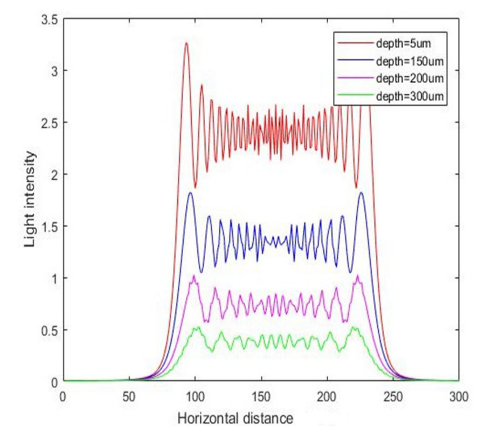
3.1. Simulation Results
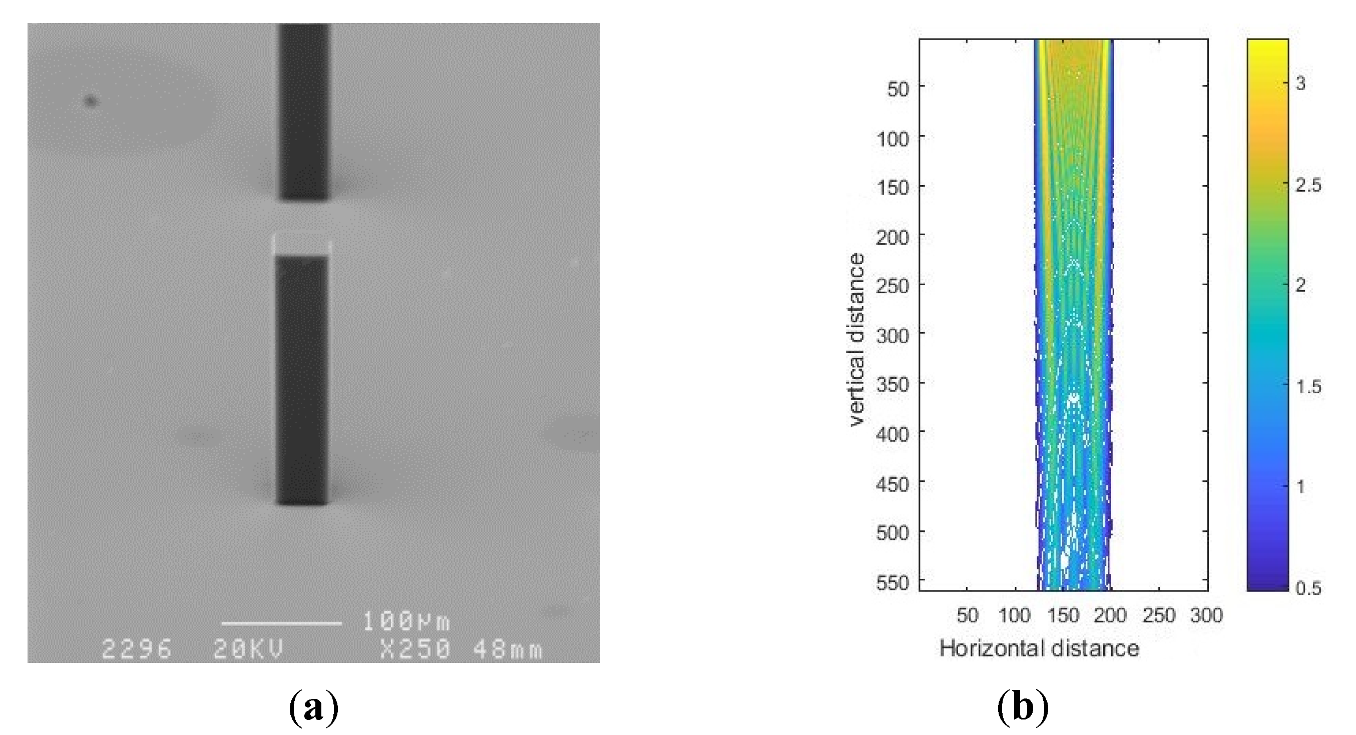
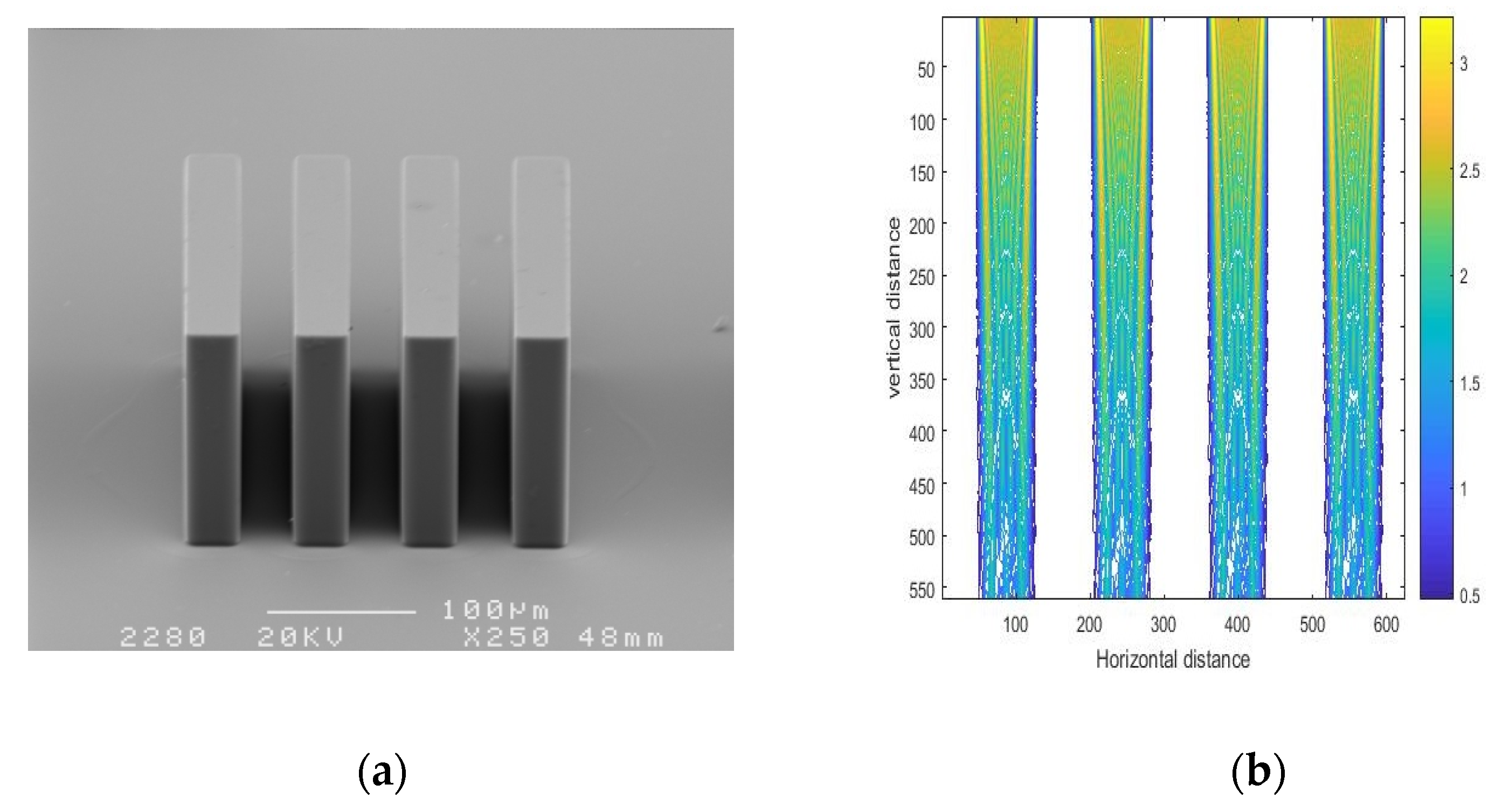
3.2. Experimental Results and Analysis
4. Conclusions
Author Contributions
Funding
Conflicts of Interest
References
- Cui, Z.; Jenkins, D.W.; Schneider, A.; McBride, G. Profile control of SU-8 photoresist using different radiation sources. In MEMS Design, Fabrication, Characterization, and Packaging; International Society for Optics and Photonics (SPIE): Bellingham, WA, USA, 2001; Volume 4407, pp. 119–126. [Google Scholar]
- Arscott, S. SU-8 as a material for lab-on-a-chip-based mass spectrometry. Lab Chip 2014, 14, 3668–3689. [Google Scholar] [CrossRef] [PubMed]
- Lorenz, H.; Despont, M.; Fahrni, N.; Brugger, J.; Vettiger, P.; Renaud, P. High-aspect-ratio, ultrathick, negative-tone near-UV photoresist and its applications for MEMS. Sens. Actuators A Phys. 1998, 64, 33–39. [Google Scholar] [CrossRef] [Green Version]
- Gray, B.L.; Lordanov, V.P.; Sarro, P.M.; Bossche, A. SU-8 Structures for Integrated High-Speed Screening. In Micro Total Analysis Systems; Baba, Y., Shoji, S., van den Berg, A., Eds.; Springer: Dordrecht, The Netherlands, 2002; pp. 464–466. [Google Scholar] [CrossRef]
- Jackman, R.J.; Floyd, T.M.; Ghodssi, R.; Schmidt, M.; Jensen, K.F. Microfluidic systems with on-line UV detection fabricated in photodefinable epoxy. J. Micromech. Microeng. 2001, 11, 263–269. [Google Scholar] [CrossRef]
- Lorenz, H.; Despont, M.; Fahrni, N.; LaBianca, N.; Renaud, P.; Vettiger, P. A low cost negative resist for MEMS. J. Micromech. Microeng. 1997, 7, 121–124. [Google Scholar] [CrossRef]
- Neureuther, A.W. Understanding Lithography Technology Issues through Simulation. Jpn. J. Appl. Phys. 1993, 32. [Google Scholar] [CrossRef]
- Levinson, H.J. Principles of Lithography; SPIE Press: Bellingham, WA, USA, 2005. [Google Scholar]
- Mack, C.A. PROLITH: A Comprehensive Optical Lithography Model. In Proceedings of the 1985 Microlithography Conferences, Santa Clara, CA, USA, 11–14 March 1985; Volume 538, pp. 207–220. [Google Scholar]
- Born, M.; Wolf, E. Principles of Optics: Electromagnetic Theory of Propagation, Interference and Diffraction of Light; Cambridge University Press: Cambridge, UK, 1999. [Google Scholar]
- Rudolph, O.H.; Evanschitzky, P.; Erdmann, A.; Bär, E.; Lorenz, J.K. Rigorous electromagnetic field simulation of the impact of photomask line-edge and line-width roughness on lithographic processes. J. Micro/Nanolithog. MEMS MOEMS 2012, 11, 013004-1. [Google Scholar] [CrossRef]
- Evanschitzky, P.; Erdmann, A. Fast near field simulation of optical and EUV masks using the waveguide method. In Proceedings of the 23rd European Mask and Lithography Conference, Grenoble, France, 22–26 January 2007. [Google Scholar]
- Erdmann, A.; Evanschitzky, P.; Citarella, G.; Fühner, T.; De Bisschop, P. Rigorous mask modeling using waveguide and FDTD methods: An assessment for typical hyper-NA imaging problems. In Photomask and Next-Generation Lithography Mask Technology XIII; International Society for Optics and Photonics (SPIE): Bellingham, WA, USA, 2006; Volume 6283, p. 628319. [Google Scholar] [CrossRef]
- Nyyssonen, D. Theory of optical edge detection and imaging of thick layers. J. Opt. Soc. Am. 1982, 72, 1425–1436. [Google Scholar] [CrossRef]
- Yuan, C.M. Calculation of one-dimensional lithographic aerial images using the vector theory. IEEE Trans. Electron Devices 1993, 40, 1604–1613. [Google Scholar] [CrossRef]
- Evanschitzky, P.; Erdmann, A. Three dimensional EUV simulations: A new mask near field and imaging simulation system. Photomask Technol. 2005, 5992. [Google Scholar] [CrossRef]
- Zhu, Z.; Lucas, K.; Cobb, J.L.; Hector, S.D.; Strojwas, A.J. Rigorous EUV mask simulator using 2D and 3D waveguide methods. In Emerging Lithographic Technologies VII; International Society for Optics and Photonics (SPIE): Bellingham, WA, USA, 2003; Volume 5037, pp. 494–503. [Google Scholar]
- Yuan, C.-M. Efficient light scattering modeling for alignment, metrology, and resist exposure in photolithography. IEEE Trans. Electron Devices 1992, 39, 1588–1598. [Google Scholar] [CrossRef]
- Lucas, K.D.; Tanabe, H.; Strojwas, A.J. Efficient and rigorous three-dimensional model for optical lithography simulation. J. Opt. Soc. Am. A 1996, 13, 2187–2199. [Google Scholar] [CrossRef]
- Schellenberg, F.M.; Adam, K.; Matteo, J.; Hesselink, L. Electromagnetic phenomena in advanced photomasks. J. Vac. Sci. Technol. B Microelectron. Nanometer Struct. 2005, 23, 3106. [Google Scholar] [CrossRef]
- Shao, F.; Evanschitzky, P.; Reibold, D.; Erdmann, A. Fast rigorous simulation of mask diffraction using the waveguide method with parallelized decomposition technique. In Proceedings of the 24th European Mask and Lithography Conference, Dresden, Germany, 21–24 January 2008. [Google Scholar]
- Tanabe, H. Modeling of optical images in resists by vector potentials. In Optical/Laser Microlithography V; International Society for Optics and Photonics (SPIE): Bellingham, WA, USA, 1992; Volume 1674, pp. 637–649. [Google Scholar]
- Yuan, C.-M.; Strojwas, A.J. Modeling optical microscope images of integrated-circuit structures. J. Opt. Soc. Am. A 1991, 8, 778. [Google Scholar] [CrossRef]
- Gaudet, M.; Arscott, S. A user-friendly guide to the optimum ultraviolet photolithographic exposure and greyscale dose of SU-8 photoresist on common MEMS, microsystems, and microelectronics coatings and materials. Anal. Methods 2017, 9, 2495–2504. [Google Scholar] [CrossRef]
- Wang, F.; Zhou, Z.; Weihua, L.; Qing’an, H. Rigorous electromagnetic field model for optical lithography simulation. High Power Laser Part. Beams 2015, 27, 024106. [Google Scholar] [CrossRef]
- Wojcik, G.L.; Vaughan, D.K.; Mould, J.J.; Leon, F.A.; Qian, Q.-D.; Lutz, M.A. Laser alignment modeling using rigorous numerical simulations. In Optical/Laser Microlithography IV; International Society for Optics and Photonics (SPIE): Bellingham, WA, USA, 1991; Volume 1463, pp. 292–303. [Google Scholar]
- Gaudet, M.; Camart, J.-C.; Buchaillot, L.; Arscott, S. Variation of absorption coefficient and determination of critical dose of SU-8 at 365 nm. Appl. Phys. Lett. 2006, 88, 24107. [Google Scholar] [CrossRef]


Publisher’s Note: MDPI stays neutral with regard to jurisdictional claims in published maps and institutional affiliations. |
© 2020 by the authors. Licensee MDPI, Basel, Switzerland. This article is an open access article distributed under the terms and conditions of the Creative Commons Attribution (CC BY) license (http://creativecommons.org/licenses/by/4.0/).
Share and Cite
Geng, Z.-C.; Zhou, Z.-F.; Dai, H.; Huang, Q.-A. A 2D Waveguide Method for Lithography Simulation of Thick SU-8 Photoresist. Micromachines 2020, 11, 972. https://doi.org/10.3390/mi11110972
Geng Z-C, Zhou Z-F, Dai H, Huang Q-A. A 2D Waveguide Method for Lithography Simulation of Thick SU-8 Photoresist. Micromachines. 2020; 11(11):972. https://doi.org/10.3390/mi11110972
Chicago/Turabian StyleGeng, Zi-Chen, Zai-Fa Zhou, Hui Dai, and Qing-An Huang. 2020. "A 2D Waveguide Method for Lithography Simulation of Thick SU-8 Photoresist" Micromachines 11, no. 11: 972. https://doi.org/10.3390/mi11110972
APA StyleGeng, Z.-C., Zhou, Z.-F., Dai, H., & Huang, Q.-A. (2020). A 2D Waveguide Method for Lithography Simulation of Thick SU-8 Photoresist. Micromachines, 11(11), 972. https://doi.org/10.3390/mi11110972