A Novel Characterization and Performance Measurement of Memristor Devices for Synaptic Emulators in Advanced Neuro-Computing

 ,
, 

Abstract
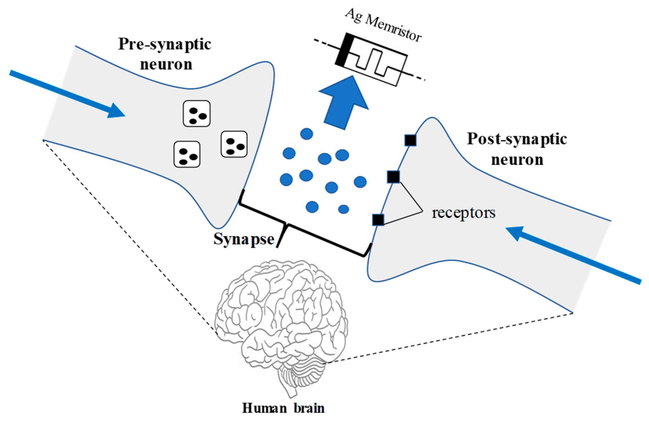
1. Introduction
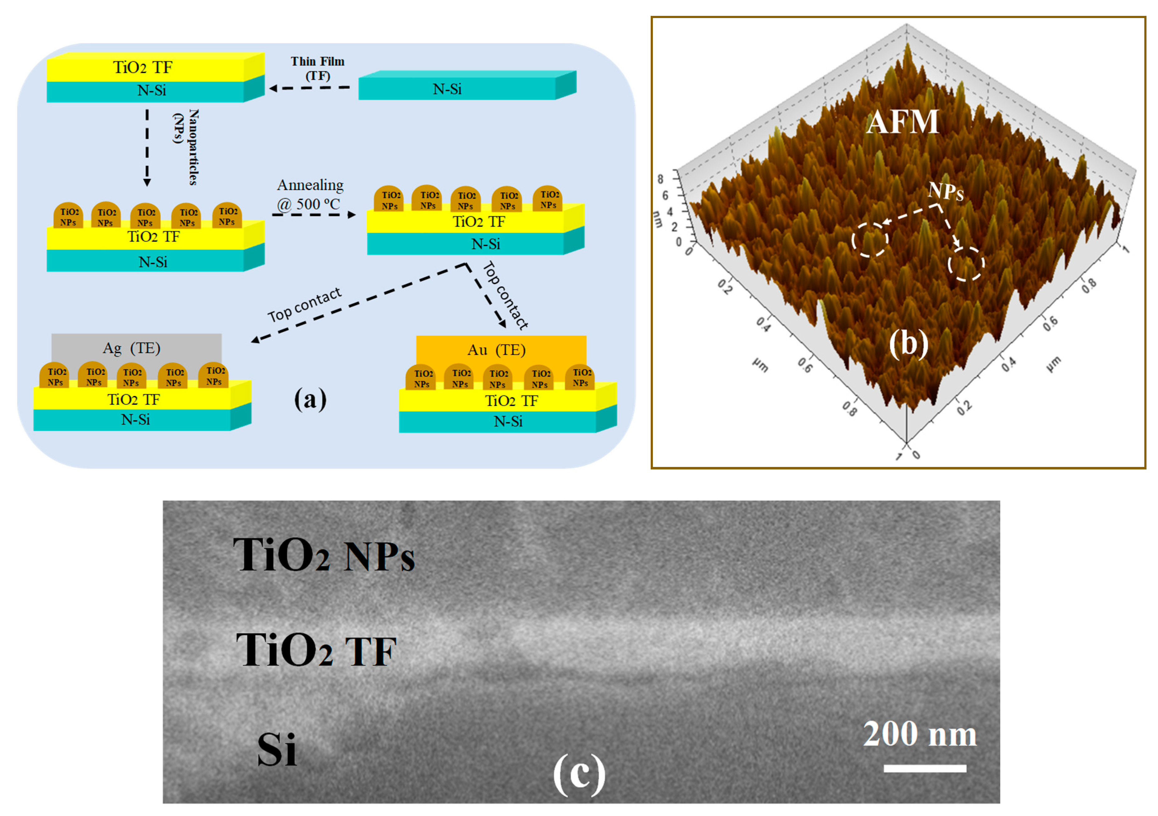
2. Materials and Methods
3. Results and Discussion
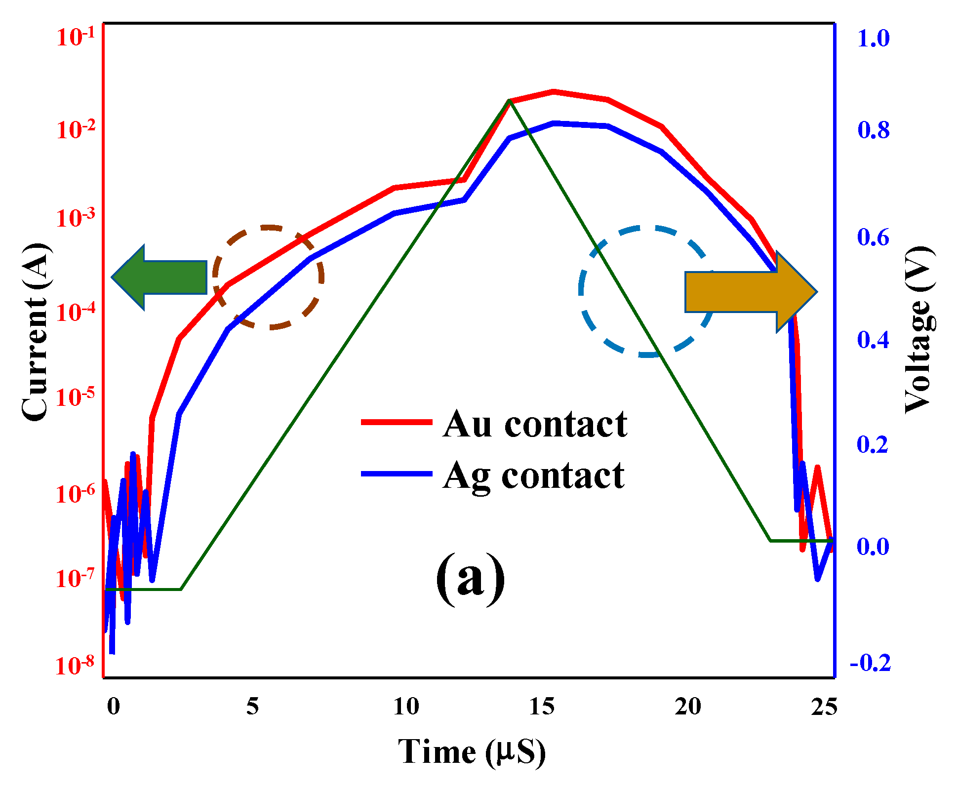
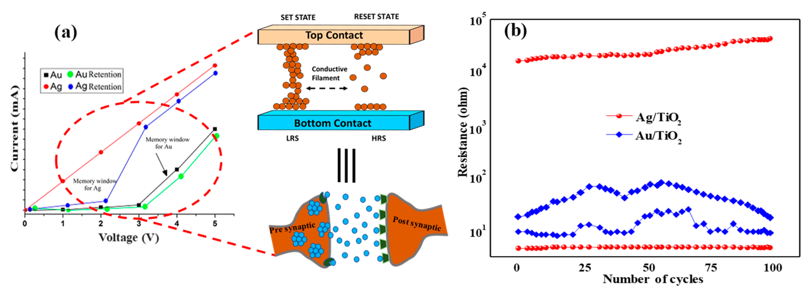
3.1. Memristors Performance
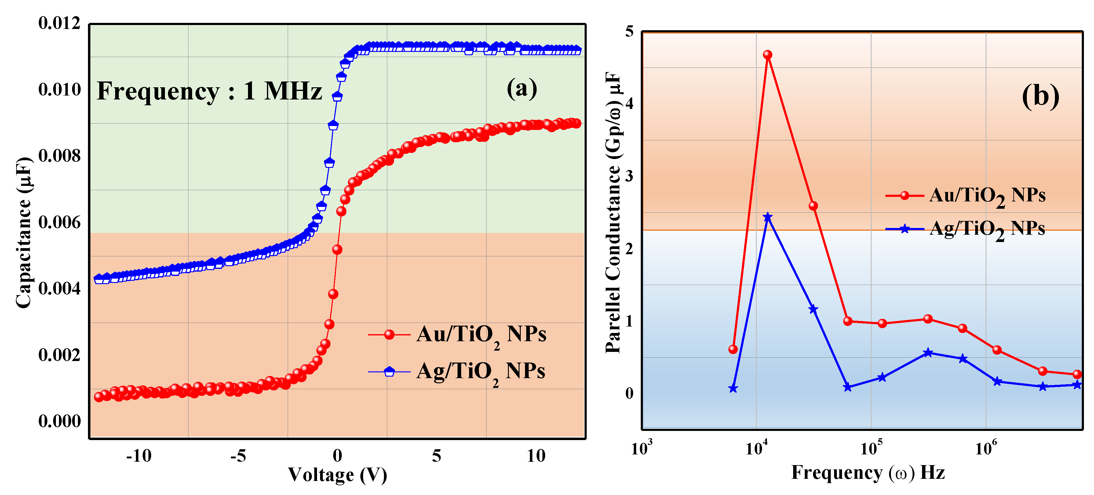
3.2. Capacitance Vs Voltage
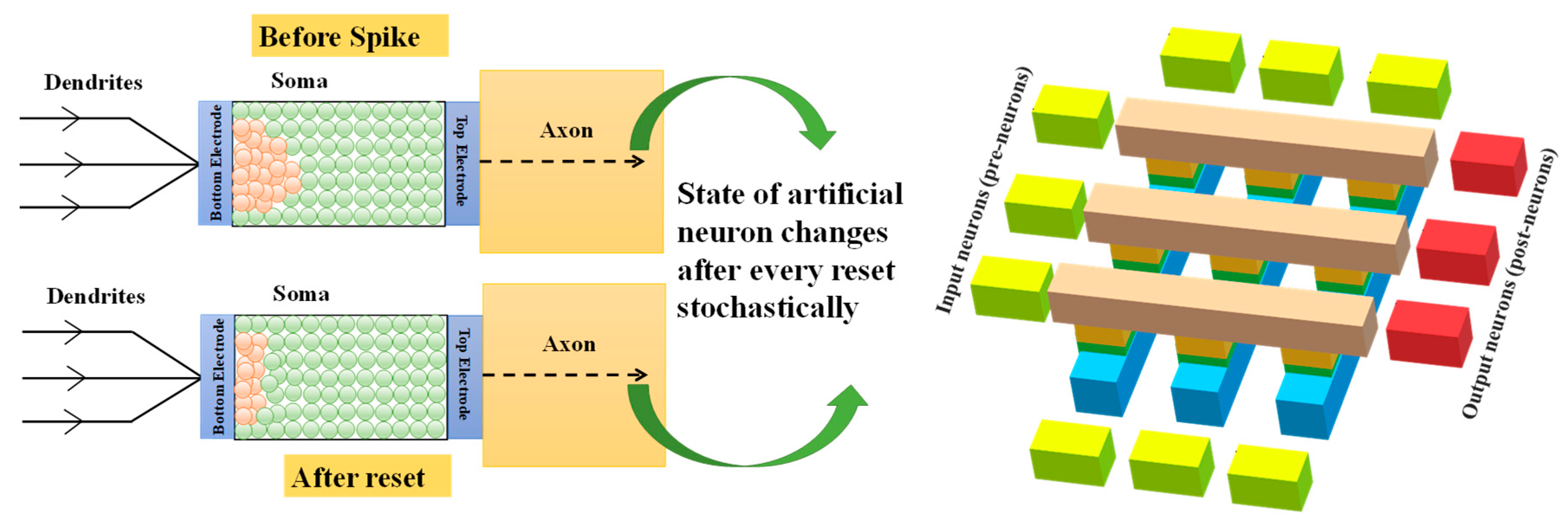
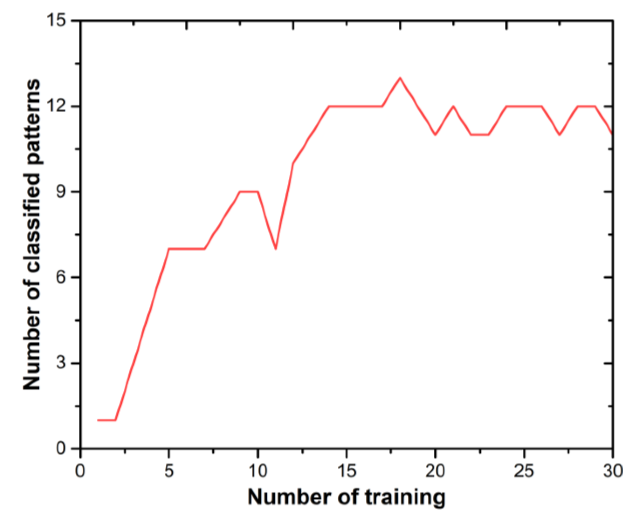
3.3. Application with Ag Based Memristor for Image Classification.
4. Conclusions
Author Contributions
Funding
Conflicts of Interest
References
- Al-Shidaifat, A.; Kumar, S.; Song, H. Voltage regulation of retina neuron model with dynamic feedback for biological acquisition image. Biochip J. 2017, 11, 300–307. [Google Scholar] [CrossRef]
- Zhang, Q.; Yu, H.; Barbiero, M.; Wang, B.; Gu, M. Artificial neural networks enabled by nanophotonics. Light Sci. Appl. 2019, 8, 42. [Google Scholar] [CrossRef] [PubMed]
- McCulloch, W.S.; Pitts, W. A logical calculus of the ideas immanent in nervous activity. Bull. Math. Biophys. 1943, 5, 115–133. [Google Scholar] [CrossRef]
- Hodgkin, A.L.; Huxley, A.F. Currents carried by sodium and potassium ions through the membrane of the giant axon of Loligo. J. Appl. Physiol. 1952, 116, 449–472. [Google Scholar] [CrossRef]
- Sun, W.; Gao, B.; Chi, M.; Xia, Q.; Yang, J.J.; Qian, H.; Wu, H. Understanding memristive switching via in situ characterization and device modeling. Nat. Commun. 2019, 10, 3453. [Google Scholar] [CrossRef] [PubMed]
- Jo, S.; Sun, W.; Kim, B.; Kim, S.; Park, J.; Shin, H. Memristor Neural Network Training with Clock Synchronous Neuromorphic System. Micromachines 2019, 10, 384. [Google Scholar] [CrossRef]
- Upadhyay, N.K.; Jiang, H.; Wang, Z.; Asapu, S.; Xia, Q.; Joshua Yang, J. Emerging Memory Devices for Neuromorphic Computing. Adv. Mater. Technol. 2019, 4, 1800589. [Google Scholar] [CrossRef]
- Hasegawa, T.; Ohno, T.; Terabe, K.; Tsuruoka, T.; Nakayama, T.; Gimzewski, J.K.; Aono, M. Learning Abilities Achieved by a Single Solid-State Atomic Switch. Adv. Mater. 2010, 22, 1831–1834. [Google Scholar] [CrossRef]
- Chua, L.O.; Sung Mo, K. Memristive devices and systems. Proc. IEEE 1976, 64, 209–223. [Google Scholar] [CrossRef]
- Choi, H.; Jung, H.; Lee, J.; Yoon, J.; Park, J.; Seong, D.-J.; Lee, W.; Hasan, M.; Jung, G.-Y.; Hwang, H. An electrically modifiable synapse array of resistive switching memory. Nanotechnology 2009, 20, 345201. [Google Scholar] [CrossRef]
- Yang, J.J.; Kobayashi, N.P.; Strachan, J.P.; Zhang, M.X.; Ohlberg, D.A.A.; Pickett, M.D.; Li, Z.; Medeiros-Ribeiro, G.; Williams, R.S. Dopant Control by Atomic Layer Deposition in Oxide Films for Memristive Switches. Chem. Mater. 2011, 23, 123–125. [Google Scholar] [CrossRef]
- Umar, A. Growth of Comb-like ZnO Nanostructures for Dye-sensitized Solar Cells Applications. Nanoscale Res. Lett. 2009, 4, 1004–1008. [Google Scholar] [CrossRef]
- Hu, S.G.; Liu, Y.; Chen, T.P.; Liu, Z.; Yu, Q.; Deng, L.J.; Yin, Y.; Hosaka, S. Emulating the Ebbinghaus forgetting curve of the human brain with a NiO-based memristor. Appl. Phys. Lett. 2013, 103, 133701. [Google Scholar] [CrossRef]
- Fan, Z.; Fan, X.; Li, A.; Dong, L. In situ forming, characterization, and transduction of nanowire memristors. Nanoscale 2013, 5, 12310–12315. [Google Scholar] [CrossRef]
- Waser, R.; Dittmann, R.; Staikov, G.; Szot, K. Redox-Based Resistive Switching Memories – Nanoionic Mechanisms, Prospects, and Challenges. Adv. Mater. 2009, 21, 2632–2663. [Google Scholar] [CrossRef]
- Seok, J.Y.; Kim, G.H.; Kim, J.H.; Kim, U.K.; Chung, Y.J.; Song, S.J.; Yoon, J.H.; Yoon, K.J.; Lee, M.H.; Kim, K.M.; et al. Resistive Switching in TiO2 Thin Films Using the Semiconducting In-Ga-Zn-O Electrode. IEEE Electron Device Lett. 2012, 33, 582–584. [Google Scholar] [CrossRef]
- Kwon, D.-H.; Kim, K.M.; Jang, J.H.; Jeon, J.M.; Lee, M.H.; Kim, G.H.; Li, X.-S.; Park, G.-S.; Lee, B.; Han, S.; et al. Atomic structure of conducting nanofilaments in TiO2 resistive switching memory. Nat. Nanotechnol. 2010, 5, 148. [Google Scholar] [CrossRef]
- McFarland, E.W.; Tang, J. A photovoltaic device structure based on internal electron emission. Nature 2003, 421, 616–618. [Google Scholar] [CrossRef]
- Kim, H.-S.; Lee, J.-W.; Yantara, N.; Boix, P.P.; Kulkarni, S.A.; Mhaisalkar, S.; Grätzel, M.; Park, N.-G. High Efficiency Solid-State Sensitized Solar Cell-Based on Submicrometer Rutile TiO2 Nanorod and CH3NH3PbI3 Perovskite Sensitizer. Nano Lett. 2013, 13, 2412–2417. [Google Scholar] [CrossRef]
- Kim, I.-D.; Rothschild, A.; Lee, B.H.; Kim, D.Y.; Jo, S.M.; Tuller, H.L. Ultrasensitive Chemiresistors Based on Electrospun TiO2 Nanofibers. Nano Lett. 2006, 6, 2009–2013. [Google Scholar] [CrossRef]
- The memristor revisited. Nat. Electron. 2018, 1, 261. [CrossRef]
- Kolka, Z.; Biolek, D.; Biolkova, V. Improved Model of TiO2 Memristor. Radioengineering 2015, 24, 378–383. [Google Scholar] [CrossRef]
- Sawa, A. Resistive switching in transition metal oxides. Mater. Today 2008, 11, 28–36. [Google Scholar] [CrossRef]
- Yang, J.J.; Pickett, M.D.; Li, X.; Ohlberg, D.A.A.; Stewart, D.R.; Williams, R.S. Memristive switching mechanism for metal/oxide/metal nanodevices. Nat. Nanotechnol. 2008, 3, 429. [Google Scholar] [CrossRef]
- Strachan, J.P.; Pickett, M.D.; Yang, J.J.; Aloni, S.; David Kilcoyne, A.L.; Medeiros-Ribeiro, G.; Stanley Williams, R. Direct Identification of the Conducting Channels in a Functioning Memristive Device. Adv. Mater. 2010, 22, 3573–3577. [Google Scholar] [CrossRef]
- Borghetti, J.; Snider, G.S.; Kuekes, P.J.; Yang, J.J.; Stewart, D.R.; Williams, R.S. ‘Memristive’ switches enable ‘stateful’ logic operations via material implication. Nature 2010, 464, 873–876. [Google Scholar] [CrossRef]
- Zhu, L.Q.; Wan, C.J.; Guo, L.Q.; Shi, Y.; Wan, Q. Artificial synapse network on inorganic proton conductor for neuromorphic systems. Nat. Commun. 2014, 5, 3158. [Google Scholar] [CrossRef]
- Chakrabartty, S.; Kumar, S.; Song, H.; Jeon, M. Ag/TiO2 NPs/TiO2 TF/Si Based Non-Volatile Memristor Device for Neuromorphic Computing Applications. J. Nanosci. Nanotechnol. 2018, 18, 7912–7916. [Google Scholar] [CrossRef]
- Chakrabartty, S.; Acharjee, S.; Al-Shidaifat, A.; Biswas, M.; Song, H. Gd-Doped HfO2 Memristor Device, Evaluation Robustness by Image Noise Cancellation and Edge Detection Filter for Neuromorphic Computing. IEEE Access 2019, 7, 157922–157932. [Google Scholar] [CrossRef]
- Martí, R. Multi-Start Methods. In Handbook of Metaheuristics; Glover, F., Kochenberger, G.A., Eds.; Springer US: Boston, MA, USA, 2003; pp. 355–368. [Google Scholar] [CrossRef]
- Cristoloveanu, S.; Li, S. Electrical Characterization of Silicon-on-Insulator Materials and Devices; Springer US: Boston, MA, USA, 1995; p. 381. [Google Scholar] [CrossRef]
- Hill, W.A.; Coleman, C.C. A single-frequency approximation for interface-state density determination. Solid State Electron. 1980, 23, 987–993. [Google Scholar] [CrossRef]


| Device | Correlation Value between Experimental Data and Statistical Fit Data | Mean Square Error between Experimental Data and Statistical Fit Data |
|---|---|---|
| Memristor with Au Contact | 0.9957 | 2.228 × 10⁻¹³ |
| Memristor with Ag Contact | 0.9952 | 2.147 × 10⁻¹² |
© 2020 by the authors. Licensee MDPI, Basel, Switzerland. This article is an open access article distributed under the terms and conditions of the Creative Commons Attribution (CC BY) license (http://creativecommons.org/licenses/by/4.0/).
Share and Cite
Al-Shidaifat, A.; Chakrabartty, S.; Kumar, S.; Acharjee, S.; Song, H. A Novel Characterization and Performance Measurement of Memristor Devices for Synaptic Emulators in Advanced Neuro-Computing. Micromachines 2020, 11, 89. https://doi.org/10.3390/mi11010089
Al-Shidaifat A, Chakrabartty S, Kumar S, Acharjee S, Song H. A Novel Characterization and Performance Measurement of Memristor Devices for Synaptic Emulators in Advanced Neuro-Computing. Micromachines. 2020; 11(1):89. https://doi.org/10.3390/mi11010089
Chicago/Turabian StyleAl-Shidaifat, AlaaDdin, Shubhro Chakrabartty, Sandeep Kumar, Suvojit Acharjee, and Hanjung Song. 2020. "A Novel Characterization and Performance Measurement of Memristor Devices for Synaptic Emulators in Advanced Neuro-Computing" Micromachines 11, no. 1: 89. https://doi.org/10.3390/mi11010089
APA StyleAl-Shidaifat, A., Chakrabartty, S., Kumar, S., Acharjee, S., & Song, H. (2020). A Novel Characterization and Performance Measurement of Memristor Devices for Synaptic Emulators in Advanced Neuro-Computing. Micromachines, 11(1), 89. https://doi.org/10.3390/mi11010089