1. Introduction
In recent times, infrared nano-plasmonics shifts its interest from common noble metals or compounds like Au, Pt, Ag or TiN [
1] to transparent conductive oxides as materials of choice [
2]—namely, indium tin oxide [
3,
4,
5,
6,
7,
8,
9], fluorine doped tin oxide [
10,
11], aluminum (or gallium) doped zinc oxide [
12,
13,
14,
15,
16,
17]. Extensive research on those materials aims at both basic properties in infrared region as well as different applications such as wavelength-selective perfect absorbers and emitters [
6,
18,
19] interacting plasmonic nano-particles [
20,
21,
22,
23], optical meta-surfaces [
19], and active tunable plasmonic devices [
7,
19,
24]. Compared to those oxide materials, niobium-doped titanium oxide (TiO
2:Nb) exhibits notable electrical and optical properties. The so-called name “transparent metal” comes from high transparency in visible light and noticeably low electrical resistivity. It also has great thermal durability, high surface smoothness, mechanical robustness, humid environment endurance and other advantages, just to name a few [
25,
26,
27,
28,
29,
30,
31,
32].
In this report, we demonstrate the use of TiO2:Nb in nanostrip and nanodisk antenna arrays for infrared plasmonic devices such as surface-enhanced infrared absorption spectroscopy (SEIRA). The nanopatterned arrays were fabricated using electron beam lithography combined with plasma etching and oxygen plasma ashing processes. The fabricated nanostrip and nanodisk antenna structures of TiO2:Nb were sequentially subjected to linearly polarized infrared light in relative transmittance measurement with Fourier transform infrared spectroscopy. Resulted plasmon resonances exposed polarization dependence and shifted to longer wavelengths as the length, width of nanostrips, or diameter of nanodisks expanded. Experiment and simulation results are in good concordance.
2. Materials and Methods
Fabrication process of niobium-doped titanium dioxide nanoantenna is demonstrated generally in
Figure 1.
At first, the Nb-doped TiO2 film was co-sputtered at room temperature with TiO2 ceramic and Nb metallic targets. Both silicon (001) and borosilicate glass were used simultaneously as sputtering substrates in every deposition. Radio frequency (RF) and direct current (DC) sputtering methods were used for TiO2 and Nb targets, respectively. The sputtering chamber (!-Miller, Shibaura Mechatronics Corporation, Yokohama, Japan) was initially evacuated down to 4.0 × 10⁻⁵ Pa as base pressure, then 19 sccm of argon and 1 sccm of oxygen gas flow was introduced into the chamber to create working pressure of about 0.3 Pa. Sputtering power was set at 200 W (RF) and 20 W (DC) for TiO2 and Nb targets, respectively. After one hour of deposition, 80-nm-thick film was obtained. Then, the as-deposited films went through vacuum thermal annealing at 600 °C for 1 h. Optical properties of TiO2:Nb thin films were characterized with Ellipsometry (SENTECH, SE 850 DUV and SENDIRA, SENTECH Instruments GmbH, Berlin, Germany) from deep ultraviolet to far infrared region.
Consequently, the samples were spin coated with negative resist NBE-22A for electron beam lithography (at 2000 rounds per minute in 60 s) and baked with hot plate (110 °C in 5 min). Electron beam lithography (ELIONIX, ELS-7500EX, ELIONIX INC, Tokyo, Japan) was used to write desired pattern onto the resist layer (
Figure 1). After pattern writing process, samples were subjected to post-baking (110 °C in 5 min), developing with NMD-3 in 60 s and rinsing with iso-propyl alcohol (IPA), and finally blow-drying with nitrogen gas gun.
Reactive ion etching (ULVAC, CE-300I, SF6 gas, 0.5 Pa, 100 W power) and oxygen plasma ashing (Mory PB-600, 300 W power in 15 min) steps were carried out to remove unnecessary surrounding TiO2:Nb nanostrips or nanodisks and wash away the remaining electron resist.
Shape and morphology of strip and disk nanostructures were investigated with scanning electron microscopy (SEM, Hitachi, SU-8400, Hitachi High-Technologies Corporation, Tokyo, Japan) and Atomic force microscope (AFM, Nanoscope 5, Bruker Corporation, Billerica, MA, USA). The silicon tips SI-DF20 (Hitachi High Technologies, Tokyo, Japan) were used at tapping mode.
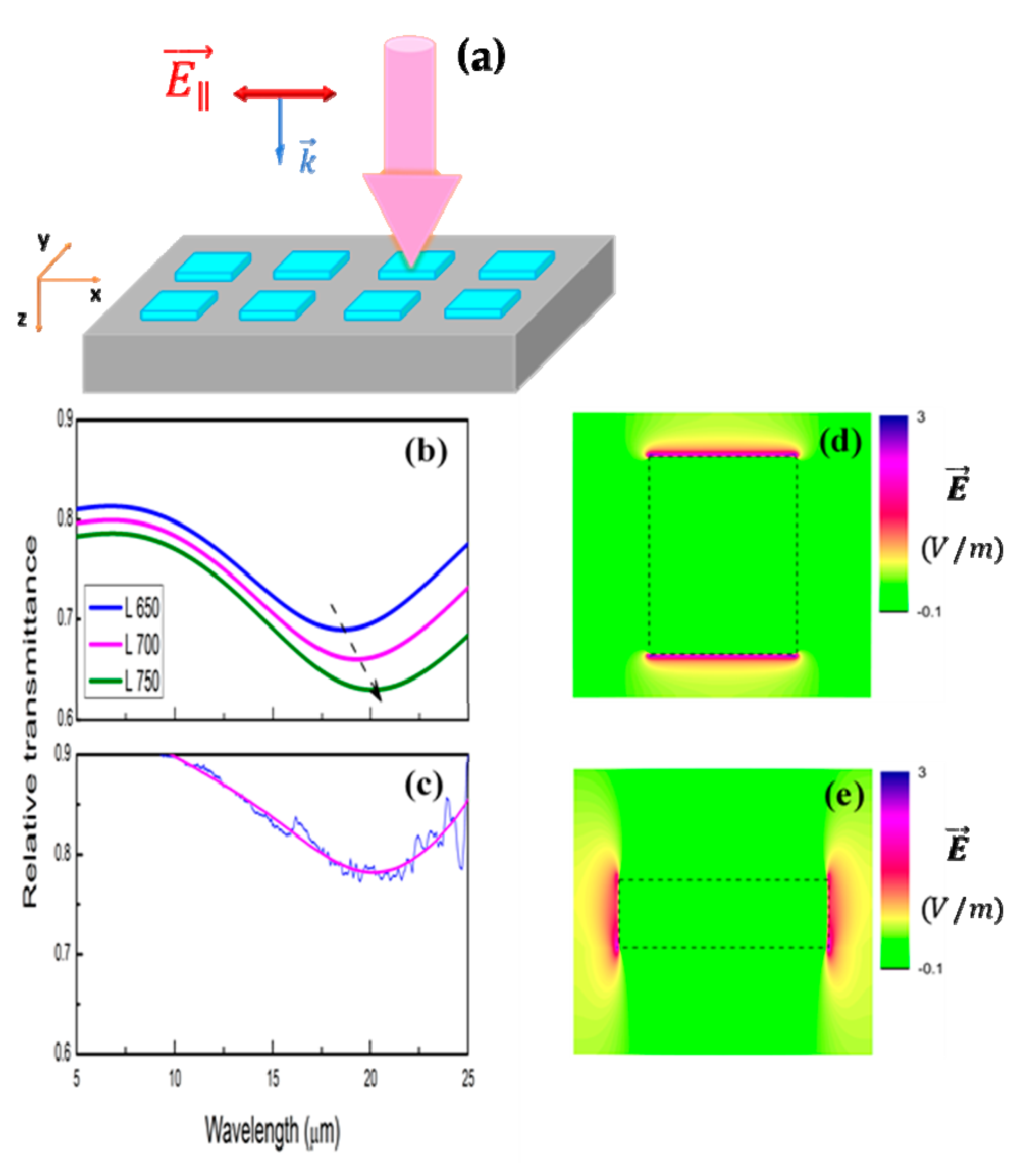
Fourier transform infrared spectroscopy (FTIR, Thermo Scientific Nicolet iS50, Waltham, MA, USA) was used to assess the resonance features of nanostructures with different linear polarization of incident light, i.e., electric field vector was either parallel to length (
) or width (
)of nanostrips, as illustrated in
Figure 2. Unpolarized incident light was used for nanodisks.
3. Results and Discussion
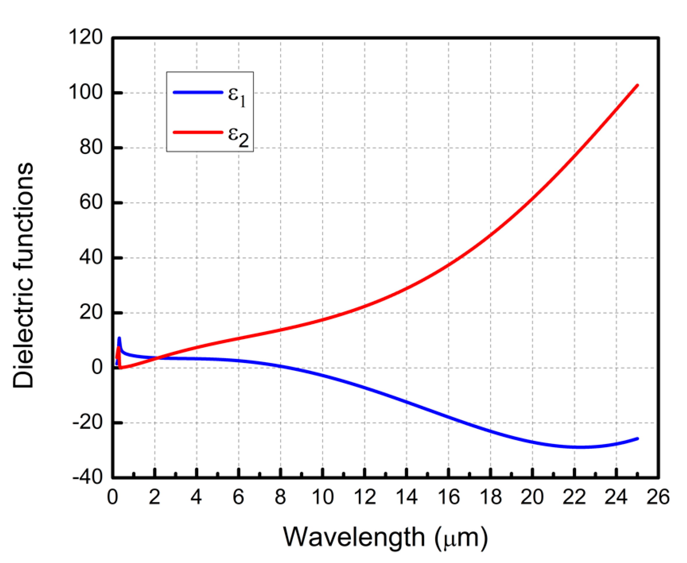
Dielectric functions (ε
1, ε
2) of co-sputtered Nb-doped TiO
2 films on silicon substrate (001) were characterized with spectroscopic ellipsometry at three different reflected angles of 60°, 65°, and 70° from ultraviolet (0.3 μm) to far infrared (25 μm) region (
Figure 3).
Real part of the dielectric function (ε1) exhibited a cross-over point in the mid-infrared region at approximately 8.5 µm. By increasing the Nb sputtering power, carrier concentration can be tuned, and Fermi level can easily be shifted toward conduction band. This in turn helps to adjust the cross-over point back and forth in the infrared region, whereas for conventional plasmonic metals such continuous tunability is not possible. Furthermore, this material also has great thermal durability, high surface smoothness, mechanical robustness, as well as photocatalytic activity and humid environment endurance. Combining altogether, TiO2:Nb film proves itself an excellent candidate for diverse infrared plasmonic applications.
To realize the plasmonic property of co-sputtered TiO
2:Nb films in infrared region, nanostrips of different sizes were simulated with electromagnetic solver to check for the antenna resonance. The simulated parameters were transferred into lithographic patterning and fabrication, and then characterized by the IR spectroscopy.
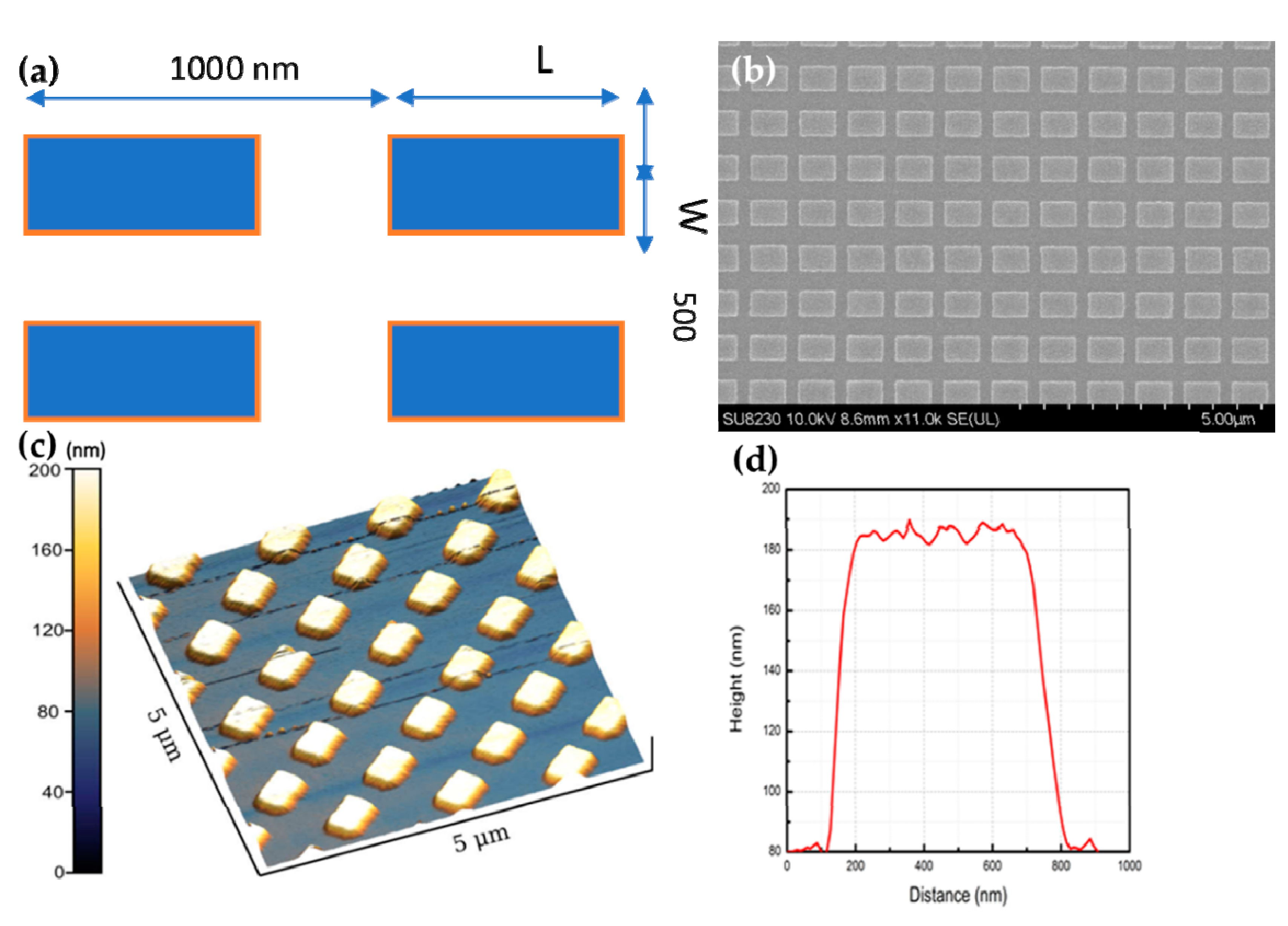
Figure 4a showed general designed nanostrip pattern used for Finite-Difference Time-Domain method (FDTD, Rsoft, Synopsis) simulation as well as electron beam lithography. In simulation, the lengths (L) of the strips were set from 650 to 750 nm while the width values (W) varied from 400 to 600 nm.
SEM and AFM images (
Figure 4b,c) show periodic rectangular nanostrips, which are similar to intended design pattern (
Figure 4a). The average strip surface roughness of 2.3 nm confirms that the etching and ashing processes did not cause considerable damage.
The smallest interval between two consecutive fabricated strips is approximately 300 nm. As illustrated in
Figure 5d and
Figure 6d, relative transmittance exhibits strong fundamental antennalike resonances as polarized electric field vector is parallel to nanostrip length or width. Both measured and simulated spectra show good agreement. Calculated spectra demonstrate orderly shift of resonances toward longer wavelengths (black dash arrow) and reveal the improvement in quality factor of nanoantenna (sharper and deeper resonances) as length or width of nanostrips increases, as in the case of metal nanowires [
32]. FDTD simulation results along x–y and x–z planes (
Figure 5d,e and
Figure 6d,e) also show strong electric field confinement and enhancement at the edges of nanostrips. This proves the antennalike dipole resonance of the structures.
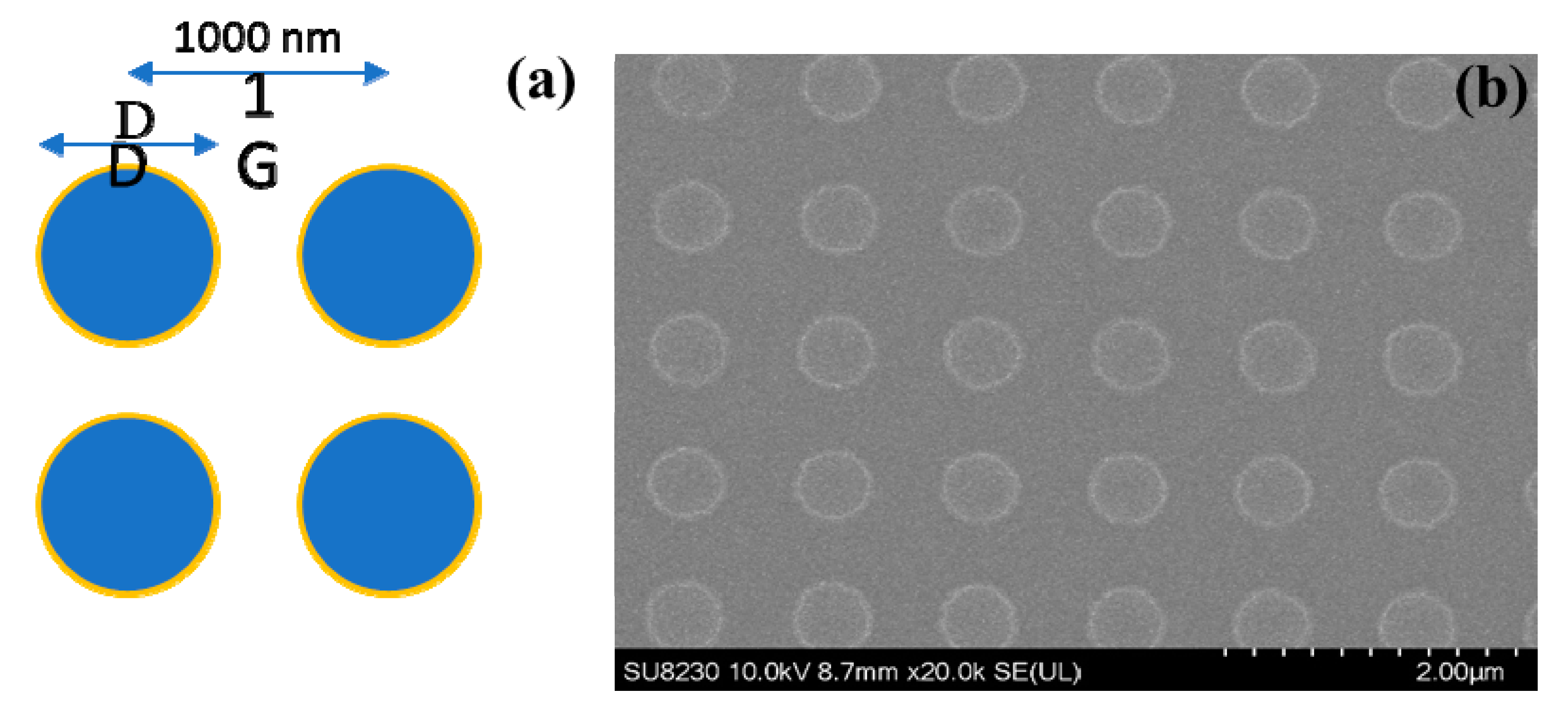
General designed nanodisk pattern for FDTD calculation and electron beam lithography was shown in
Figure 7a. Diameters of nanodisks (D) were set from 600 to 800 nm.
In simulated results, systematic increase of resonance frequency with diameter (D) can be easily observed. Sharper resonances can be expected if disk diameter keeps expanding. Experimental relative transmittance spectrum is in consonance with calculated lines with strong fundamental antennalike resonances under any linear polarized infrared light parallel to the disk surface (
Figure 8d). Quality factor of these nanodisk antennae can be further improved when the diameter D increases since the surface plasmon resonance assumes more photonic nature and the inherent loss of the material becomes less. While resonant frequencies show good matching between simulation and experiment curves in x axis; there is some difference (~10% to 15%) in relative transmittance (
y-axis). This can be explained by two factors: fabrication tolerance and etchant effect. Perfect cuboids were used in simulation, but the obtained ones were not perfectly flat at edges, as shown in
Figure 4c,d. Furthermore, electron carrier concentration was decreased from 1.12 × 10
21 cm
−3 for pristine film to 6.4 × 10
20 cm
−3 for remained one. SF
6 gas may introduce some electron-trapping fluorine ions on surface of nanostructure after etching.
4. Conclusions
We succeeded in designing and fabricating antenna arrays of nanostrips and nanodisks based on Nb doped TiO2. Relative infrared transmittance in calculated and experimental results are in good accordance. Spectral features exhibit red-shift in their peak position as the sizes of strips and disks increase. In the same tendency, quality factor of nanostrips and nanodisks can also be improved if structure dimension can be further extended.
Author Contributions
Conceptualization, T.N.; methodology, H.D.N., K.C., A.O. and N.I.; software, A.T.D., T.D.N.; validation, and T.D.D.; formal analysis, H.D.N.; investigation, H.D.N., K.C.; data curation, H.D.N.; writing—original draft preparation, H.D.N.; writing—review and editing, H.D.N. and Ø.S.H.; visualization, H.D.N., A.T.D.; supervision, T.N.; project administration, T.N.; funding acquisition, T.N. All authors have read and agreed to the published version of the manuscript.
Funding
T.N. acknowledges the support from CREST under the project of “Phase Interface Science for Highly Efficient Energy Utilization” (JPMJCR13C3, Japan Science and Technology Agency). T.N. also acknowledge the support from JSPS KAKENHI Grant Numbers 16H06364.
Acknowledgments
We thank Tomoko Ohki and Katsumi Ohno at Nanotechnology Innovation Station, National Institute for Materials Science, for their kind help.
Conflicts of Interest
There are no conflicts of interest to declare.
References
- Sugavaneshwar, R.P.; Ishii, S.; Dao, T.D.; Ohi, A.; Nabatame, T.; Nagao, T. Fabrication of Highly Metallic TiN Films by Pulsed Laser Deposition Method for Plasmonic Applications. ACS Photonics 2018, 5, 814–819. [Google Scholar] [CrossRef]
- Kim, J.; Naik, G.V.; Emani, N.K.; Guler, U.; Boltasseva, A. Plasmonic Resonances in Nanostructured Transparent Conducting Oxide Films. IEEE J. Sel. Top. Quantum Electron. 2013, 19, 4601907. [Google Scholar]
- Wang, Y.; Overvig, A.C.; Shrestha, S.; Zhang, R.; Wang, R.; Yu, N.; Dal Negro, L. Tunability of indium tin oxide materials for mid-infrared plasmonics applications. Opt. Mater. Express 2017, 7, 2727–2739. [Google Scholar] [CrossRef]
- Li, S.Q.; Guo, P.; Zhang, L.; Zhou, W.; Odom, T.W.; Seideman, T.; Ketterson, J.B.; Chang, R.P.H. Infrared Plasmonics with Indium–Tin-Oxide Nanorod Arrays. ACS Nano 2011, 5, 9161–9170. [Google Scholar] [CrossRef] [PubMed]
- Rhodes, C.; Cerruti, M.; Efremenko, A.; Losego, M.; Aspnes, D.E.; Maria, J.-P.; Franzen, S. Dependence of plasmon polaritons on the thickness of indium tin oxide thin films. J. Appl. Phys. 2008, 103, 93108. [Google Scholar] [CrossRef]
- Tamanai, A.; Dao, T.D.; Sendner, M.; Nagao, T.; Pucci, A. Mid-infrared optical and electrical properties of indium tin oxide films. Phys. Status Solidi 2017, 214, 1600467. [Google Scholar] [CrossRef]
- Guo, P.; Schaller, R.D.; Ketterson, J.B.; Chang, R.P.H. Ultrafast switching of tunable infrared plasmons in indium tin oxide nanorod arrays with large absolute amplitude. Nat. Photonics 2016, 10, 267. [Google Scholar] [CrossRef]
- Fang, X.; Mak, C.L.; Dai, J.; Li, K.; Ye, H.; Leung, C.W. ITO/Au/ITO Sandwich Structure for Near-Infrared Plasmonics. ACS Appl. Mater. Interfaces 2014, 6, 15743–15752. [Google Scholar] [CrossRef]
- Krasilnikova Sytchkova, A.; Grilli, M.L.; Boycheva, S.; Piegari, A. Optical, electrical, structural and microstructural characteristics of rf sputtered ITO films developed for art protection coatings. Appl. Phys. A 2007, 89, 63–72. [Google Scholar] [CrossRef]
- Khalilzadeh-Rezaie, F.; Oladeji, I.O.; Cleary, J.W.; Nader, N.; Nath, J.; Rezadad, I.; Peale, R.E. Fluorine-doped tin oxides for mid-infrared plasmonics. Opt. Mater. Express 2015, 5, 2184–2192. [Google Scholar] [CrossRef]
- Dominici, L.; Michelotti, F.; Brown, T.M.; Reale, A.; Carlo, A. Di Plasmon polaritons in the near infrared on fluorine doped tin oxide films. Opt. Express 2009, 17, 10155–10167. [Google Scholar] [CrossRef] [PubMed]
- Naik, G.V.; Liu, J.; Kildishev, A.V.; Shalaev, V.M.; Boltasseva, A. Demonstration of Al:ZnO as a plasmonic component for near-infrared metamaterials. Proc. Natl. Acad. Sci. USA 2012, 109, 8834–8838. [Google Scholar] [CrossRef] [PubMed]
- Buonsanti, R.; Llordes, A.; Aloni, S.; Helms, B.A.; Milliron, D.J. Tunable Infrared Absorption and Visible Transparency of Colloidal Aluminum-Doped Zinc Oxide Nanocrystals. Nano Lett. 2011, 11, 4706–4710. [Google Scholar] [CrossRef] [PubMed]
- Kim, J.; Naik, G.V.; Gavrilenko, A.V.; Dondapati, K.; Gavrilenko, V.I.; Prokes, S.M.; Glembocki, O.J.; Shalaev, V.M.; Boltasseva, A. Optical Properties of Gallium-Doped Zinc Oxide—A Low-Loss Plasmonic Material: First-Principles Theory and Experiment. Phys. Rev. X 2013, 3, 041037. [Google Scholar] [CrossRef]
- Hendrickson, J.R.; Vangala, S.; Nader, N.; Leedy, K.; Guo, J.; Cleary, J.W. Plasmon resonance and perfect light absorption in subwavelength trench arrays etched in gallium-doped zinc oxide film. Appl. Phys. Lett. 2015, 107, 191906. [Google Scholar] [CrossRef]
- Sachet, E.; Losego, M.D.; Guske, J.; Franzen, S.; Maria, J.-P. Mid-infrared surface plasmon resonance in zinc oxide semiconductor thin films. Appl. Phys. Lett. 2013, 102, 051111. [Google Scholar] [CrossRef]
- Pradhan, A.K.; Mundle, R.M.; Santiago, K.; Skuza, J.R.; Xiao, B.; Song, K.D.; Bahoura, M.; Cheaito, R.; Hopkins, P.E. Extreme tunability in aluminum doped Zinc Oxide plasmonic materials for near-infrared applications. Sci. Rep. 2014, 4, 6415. [Google Scholar] [CrossRef]
- Kesim, Y.E.; Battal, E.; Okyay, A.K. Plasmonic materials based on ZnO films and their potential for developing broadband middle-infrared absorbers. AIP Adv. 2014, 4, 077106. [Google Scholar] [CrossRef]
- Dao, T.D.; Doan, A.T.; Ngo, D.H.; Chen, K.; Ishii, S.; Tamanai, A.; Nagao, T. Selective thermal emitters with infrared plasmonic indium tin oxide working in the atmosphere. Opt. Mater. Express 2019, 9, 2534–2544. [Google Scholar] [CrossRef]
- Kanehara, M.; Koike, H.; Yoshinaga, T.; Teranishi, T. Indium Tin Oxide Nanoparticles with Compositionally Tunable Surface Plasmon Resonance Frequencies in the Near-IR Region. J. Am. Chem. Soc. 2009, 131, 17736–17737. [Google Scholar] [CrossRef]
- Wang, T.; Radovanovic, P.V. Free Electron Concentration in Colloidal Indium Tin Oxide Nanocrystals Determined by Their Size and Structure. J. Phys. Chem. C 2011, 115, 406–413. [Google Scholar] [CrossRef]
- Xi, M.; Reinhard, B.M. Localized Surface Plasmon Coupling between Mid-IR-Resonant ITO Nanocrystals. J. Phys. Chem. C 2018, 122, 5698–5704. [Google Scholar] [CrossRef] [PubMed]
- Chen, K.; Guo, P.; Dao, T.D.; Li, S.-Q.; Ishii, S.; Nagao, T.; Chang, R.P.H. Protein-Functionalized Indium-Tin Oxide Nanoantenna Arrays for Selective Infrared Biosensing. Adv. Opt. Mater. 2017, 5, 1700091. [Google Scholar] [CrossRef]
- Liu, X.; Kang, J.-H.; Yuan, H.; Park, J.; Kim, S.J.; Cui, Y.; Hwang, H.Y.; Brongersma, M.L. Electrical tuning of a quantum plasmonic resonance. Nat. Nanotechnol. 2017, 12, 866. [Google Scholar] [CrossRef]
- Furubayashi, Y.; Hitosugi, T.; Yamamoto, Y.; Inaba, K.; Kinoda, G.; Hirose, Y.; Shimada, T.; Hasegawa, T. A transparent metal: Nb-doped anatase TiO2. Appl. Phys. Lett. 2005, 86, 252101. [Google Scholar] [CrossRef]
- Zhang, S.X.; Kundaliya, D.C.; Yu, W.; Dhar, S.; Young, S.Y.; Salamanca-Riba, L.G.; Ogale, S.B.; Vispute, R.D.; Venkatesan, T. Niobium doped TiO2: Intrinsic transparent metallic anatase versus highly resistive rutile phase. J. Appl. Phys. 2007, 102, 013701. [Google Scholar] [CrossRef]
- Baumard, J.F.; Tani, E. Electrical conductivity and charge compensation in Nb doped TiO2 rutile. J. Chem. Phys. 1977, 67, 857–860. [Google Scholar] [CrossRef]
- Lee, H.-Y.; Robertson, J. Doping and compensation in Nb-doped anatase and rutile TiO2. J. Appl. Phys. 2013, 113, 213706. [Google Scholar] [CrossRef]
- Arbiol, J.; Cerdà, J.; Dezanneau, G.; Cirera, A.; Peiró, F.; Cornet, A.; Morante, J.R. Effects of Nb doping on the TiO2 anatase-to-rutile phase transition. J. Appl. Phys. 2002, 92, 853–861. [Google Scholar] [CrossRef]
- Yamada, N.; Hitosugi, T.; Kasai, J.; Hoang, N.L.H.; Nakao, S.; Hirose, Y.; Shimada, T.; Hasegawa, T. Direct growth of transparent conducting Nb-doped anatase TiO2 polycrystalline films on glass. J. Appl. Phys. 2009, 105, 123702. [Google Scholar] [CrossRef]
- Jaćimović, J.; Gaál, R.; Magrez, A.; Piatek, J.; Forró, L.; Nakao, S.; Hirose, Y.; Hasegawa, T. Low temperature resistivity, thermoelectricity, and power factor of Nb doped anatase TiO2. Appl. Phys. Lett. 2013, 102, 013901. [Google Scholar]
- Neubrech, F.; Kolb, T.; Lovrincic, R.; Fahsold, G.; Pucci, A.; Aizpurua, J.; Cornelius, T.W.; Toimil-Molares, M.E.; Neumann, R.; Karim, S. Resonances of individual metal nanowires in the infrared. Appl. Phys. Lett. 2006, 89, 253104. [Google Scholar] [CrossRef]
Figure 1.
Fabrication process of Nb-doped TiO2 nanoantenna (from left to right) consists of electron beam lithography, development, dry etching with SF6 gas, and oxygen plasma ashing. The electron resist layer (brown) was coated on TiO2:Nb thin film (blue), which was deposited on silicon substrate (grey). The remained electron resist layer (green) after lithography process helped to define the nanostrip and nanodisk of antenna structures.
Figure 2.
Transmission measurement setup with Fourier transform infrared spectrometer. Unpolarized incident infrared light (right side) passed through polarizer (P), aperture (A) and then exposed to nanostrip sample (S) before entering the detector (D). In case of nanodisk sample, polarizer (P) was removed and unpolarized infrared light was used.
Figure 3.
Experimental dielectric functions of TiO2:Nb films on silicon substrate. Real (ε1) and imaginary (ε2) parts in blue and red curves, respectively.
Figure 3.
Experimental dielectric functions of TiO2:Nb films on silicon substrate. Real (ε1) and imaginary (ε2) parts in blue and red curves, respectively.
Figure 4.
Design patterns of TiO2:Nb antenna for simulation and electron beam lithography (a). Horizontal periodicity is 1000 nm. Strip width (W) is about 500 nm. SEM image of TiO2:Nb nanostrips (b). Three-dimensional AFM image (5 μm × 5 μm) of TiO2:Nb nanostrips (c). Height profile of a single nanostrip (d).
Figure 5.
Schematic illustration of the exposure of polarized infrared light with electric field vector (k) parallel to length of nanostrips () (a). Simulation (b) and FTIR relative transmittance (c) of nanostrips with () polarized incident light. Lengths of nanostrips (L) in simulation were set at 650, 700, and 750 nm, corresponding to blue, pink, and green curves (b). Measured and fitted lines were drawn in blue and pink, respectively (L × W ~ 750 nm × 500 nm) (c). Electric field distribution along x–y and x–z planes of strips (d, e).
Figure 6.
Schematic illustration of polarized infrared light with electric field vector parallel to the longer axis of nanostrips () (a). Simulation (b) and FTIR relative transmittance (c) of nanostrips with () polarized incident light. Widths of nanostrips (W) in simulation were set at 400, 500, and 600 nm, corresponding to red, blue, and pink curves (b). Measured spectrum was plotted in green line (L × W ~ 700 nm × 450 nm) (c). Electric field distribution along x-y and x-z planes of strips (d, e).
Figure 7.
Design patterns of TiO2:Nb nanodisk antennas for calculation and fabrication. Periodicity is 1000 nm (a). SEM image of TiO2:Nb nanodisk structure (b).
Figure 7.
Design patterns of TiO2:Nb nanodisk antennas for calculation and fabrication. Periodicity is 1000 nm (a). SEM image of TiO2:Nb nanodisk structure (b).
Figure 8.
Schematic diagram of unpolarized infrared light on nanodisk antenna structures (a). Simulation (b) and FTIR relative transmittance (c) of nanodisk with unpolarized incident light. Diameters of nanodisks (D) in simulation were set at 600, 700, and 800 nm, corresponding to blue, pink, and green curves. Measured and fitted lines were drawn in blue and red (D ~750 nm) (c). Electric field distribution along x–y and x–z planes (d, e).
© 2019 by the authors. Licensee MDPI, Basel, Switzerland. This article is an open access article distributed under the terms and conditions of the Creative Commons Attribution (CC BY) license (http://creativecommons.org/licenses/by/4.0/).

 ,
, 


