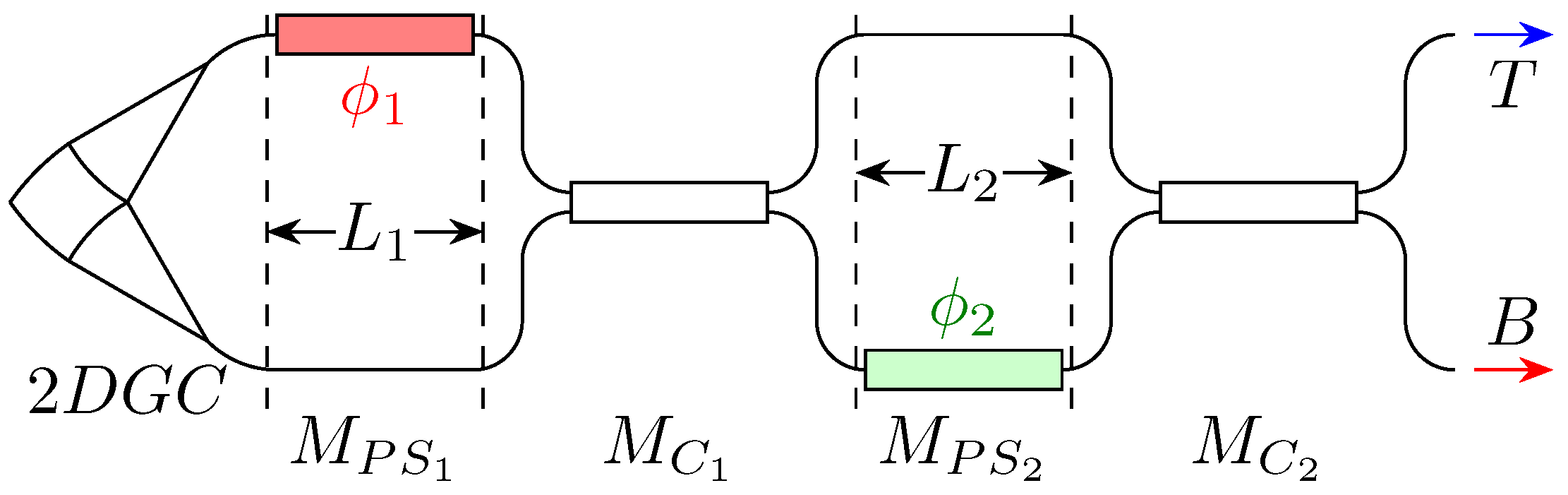
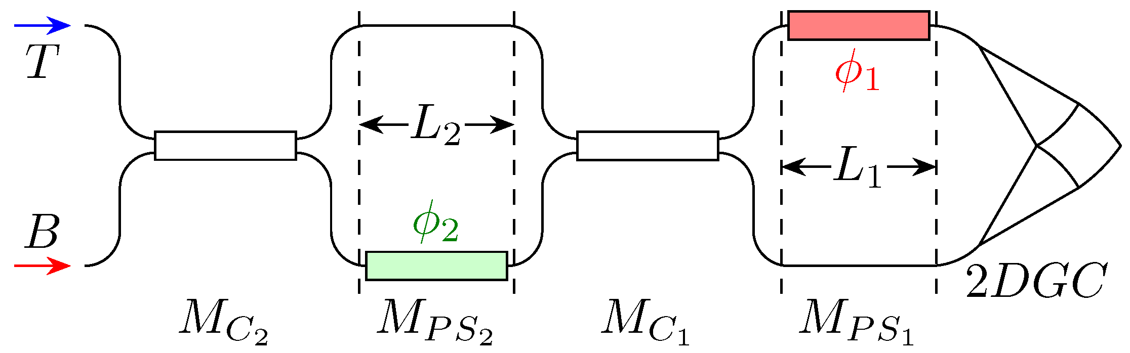
Figure 1.
Schematic of the integrated polarisation controller. The labels refer to the transfer matrix associated with a given circuit section. The block on the picture leftmost portion is a schematic of the 2DGC. The “T” and “B” labels denote the top and bottom outputs, respectively.
Figure 1.
Schematic of the integrated polarisation controller. The labels refer to the transfer matrix associated with a given circuit section. The block on the picture leftmost portion is a schematic of the 2DGC. The “T” and “B” labels denote the top and bottom outputs, respectively.
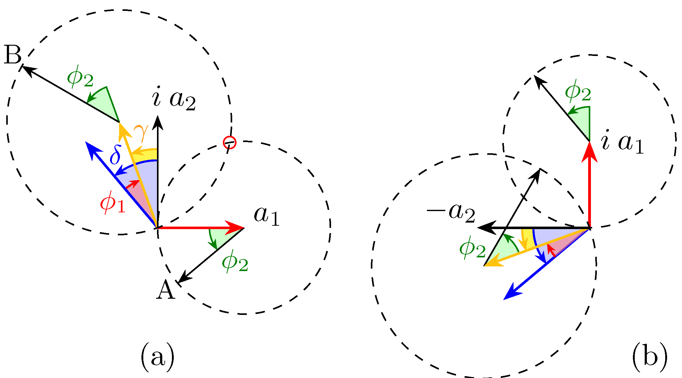
Figure 2.
Phasor diagrams for the two components of ; actually, it shows the difference, not the sum, of the two terms of each component, as it is easier to visualise. (a) Top component of Equation (4). When the tips of the two vectors lie in the second intersection, circled in red, between the circumferences, then the first component of is zero. (b) Bottom component.
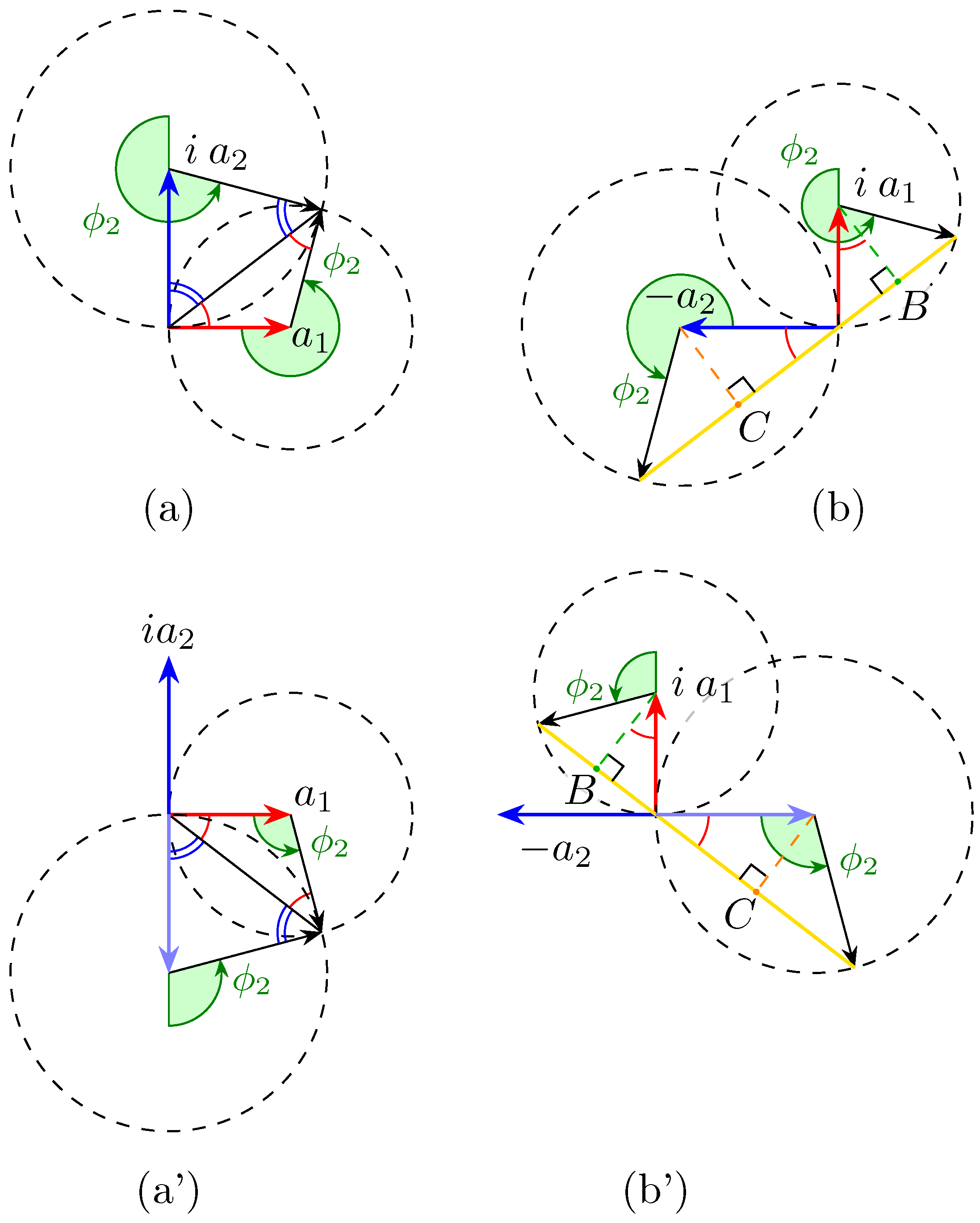
Figure 3.
Phasor diagrams for the two components of , when both conditions of Equation (6) and (7) are fulfilled. (a) The four vectors form a quadrilateral. Note that Equation (7) can be deduced observing that the quadrilateral is the union of two congruent rectangle triangles with catheti and and thus the green angle equals twice (or the explementary angle, for a’, when is odd). (b) When Equation (6) is fulfilled, then the segments joining the origin with the points on the circumferences lie on the same line. The construction in figure shows that, when Equation (7) holds too, the segment between those two points is twice the hypotenuse of the rectangle triangle with and as catheti, which corresponds to the norm (power) of the input vector. Notice that, if one of the two angles (but not both) is changed by , then the role in (a) and (b) gets reversed, i.e., the whole power goes in the top port.
Figure 4.
Plot of (a) and (b) .
Figure 4.
Plot of (a) and (b) .
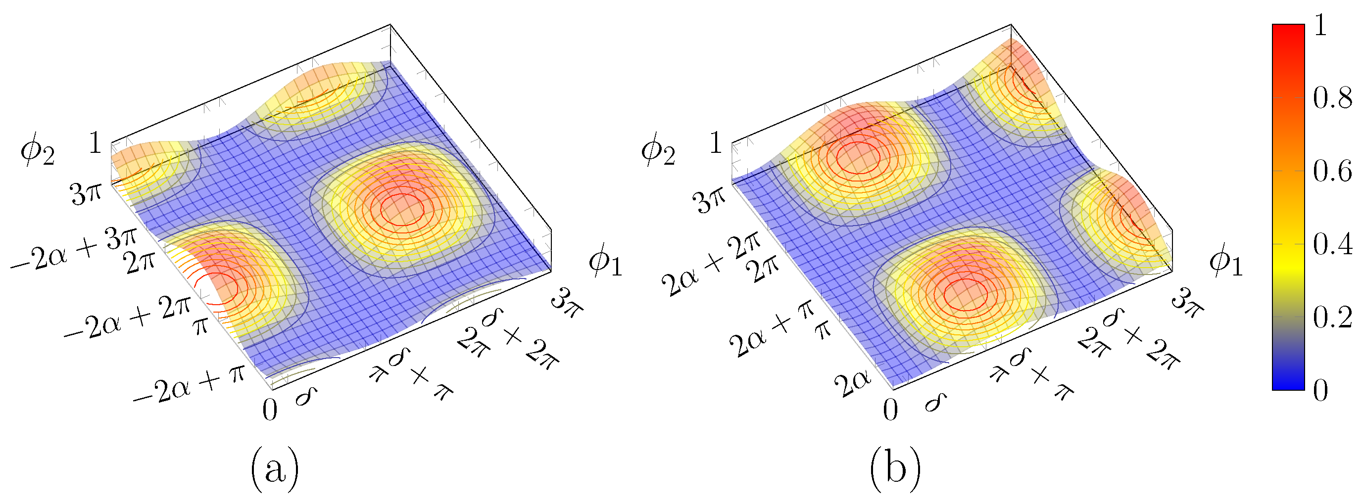
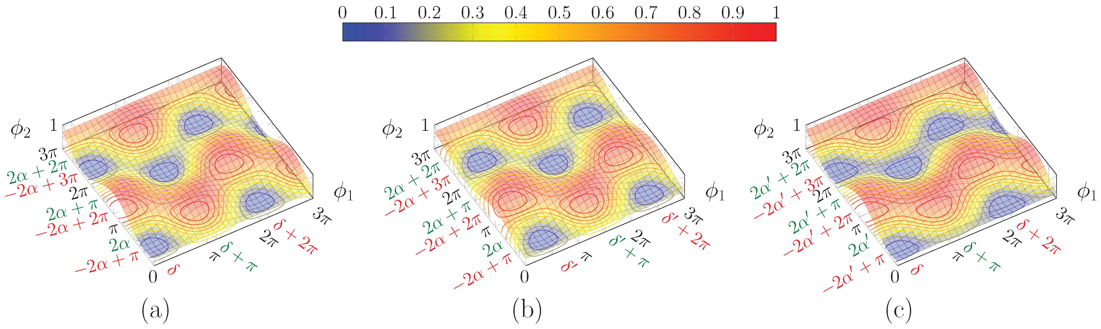
Figure 5.
Plot of for: (a) and ; (b) same but , where the surface is shifted along , but retains the same shape as (a); and (c) but same as in (a). Note that the surface has a different shape with respect to (a), even though the extrema lie in the same values. Red and green ticks correspond to the first and second solution classes, respectively.
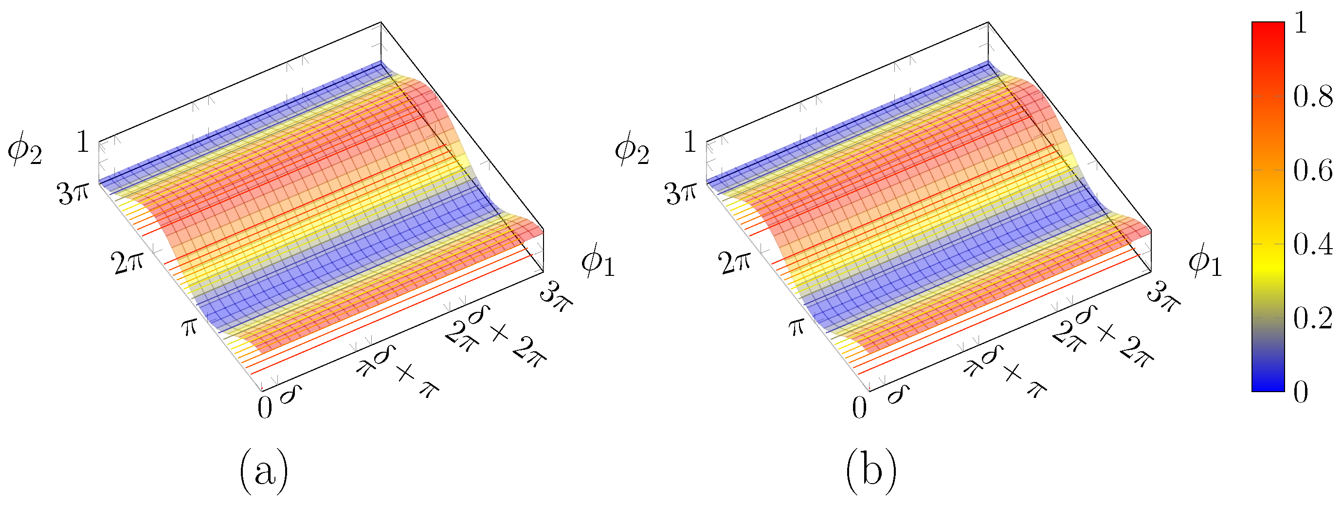
Figure 6.
Plot of for: (a) ; and (b) .
Figure 6.
Plot of for: (a) ; and (b) .
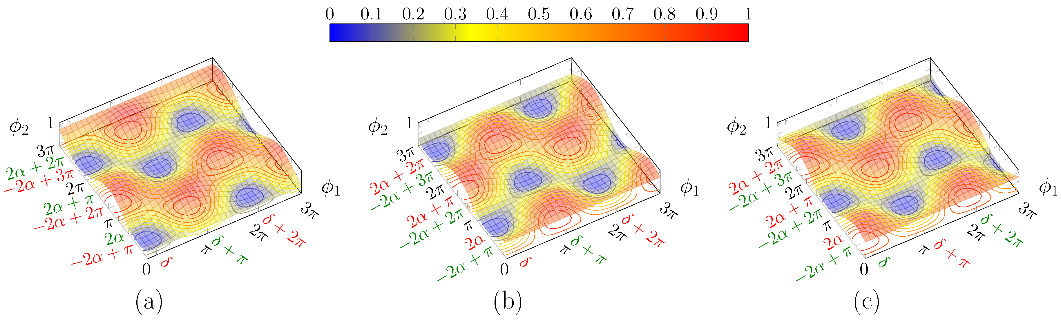
Figure 7.
Plot of for: (a) and ; (b) and same ; and (c) and . This is the complementary surface of (a). Note that the two solution classes are now inverted.
Figure 7.
Plot of for: (a) and ; (b) and same ; and (c) and . This is the complementary surface of (a). Note that the two solution classes are now inverted.
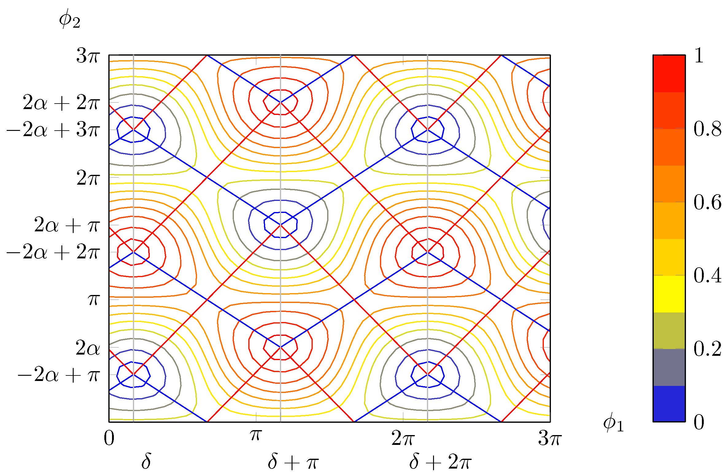
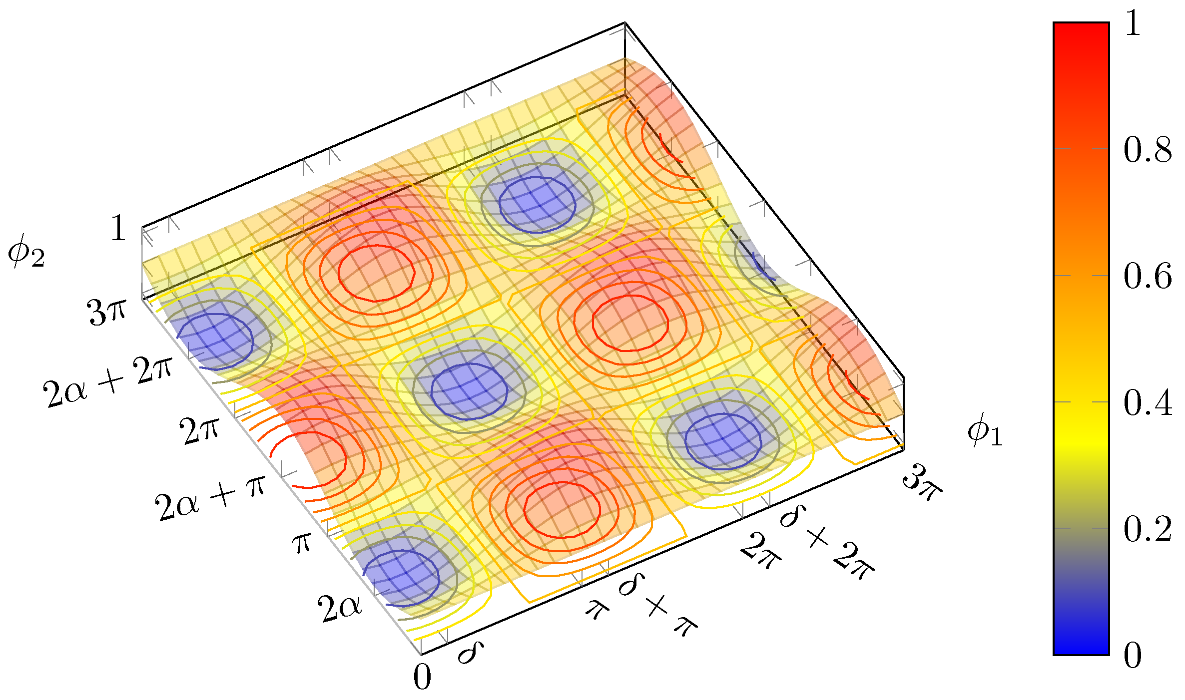
Figure 8.
Contour plot for and . In general, maxima and minima are not placed on a square grid. Blue lines join maxima lying on the same “ridge” or minima in the same “valley”, whereas red lines connect maxima separated by a “valley” or minima with a “ridge” in between, respectively.
Figure 8.
Contour plot for and . In general, maxima and minima are not placed on a square grid. Blue lines join maxima lying on the same “ridge” or minima in the same “valley”, whereas red lines connect maxima separated by a “valley” or minima with a “ridge” in between, respectively.
Figure 9.
Plot of for and . Note that now the surface displays a check pattern.
Figure 9.
Plot of for and . Note that now the surface displays a check pattern.
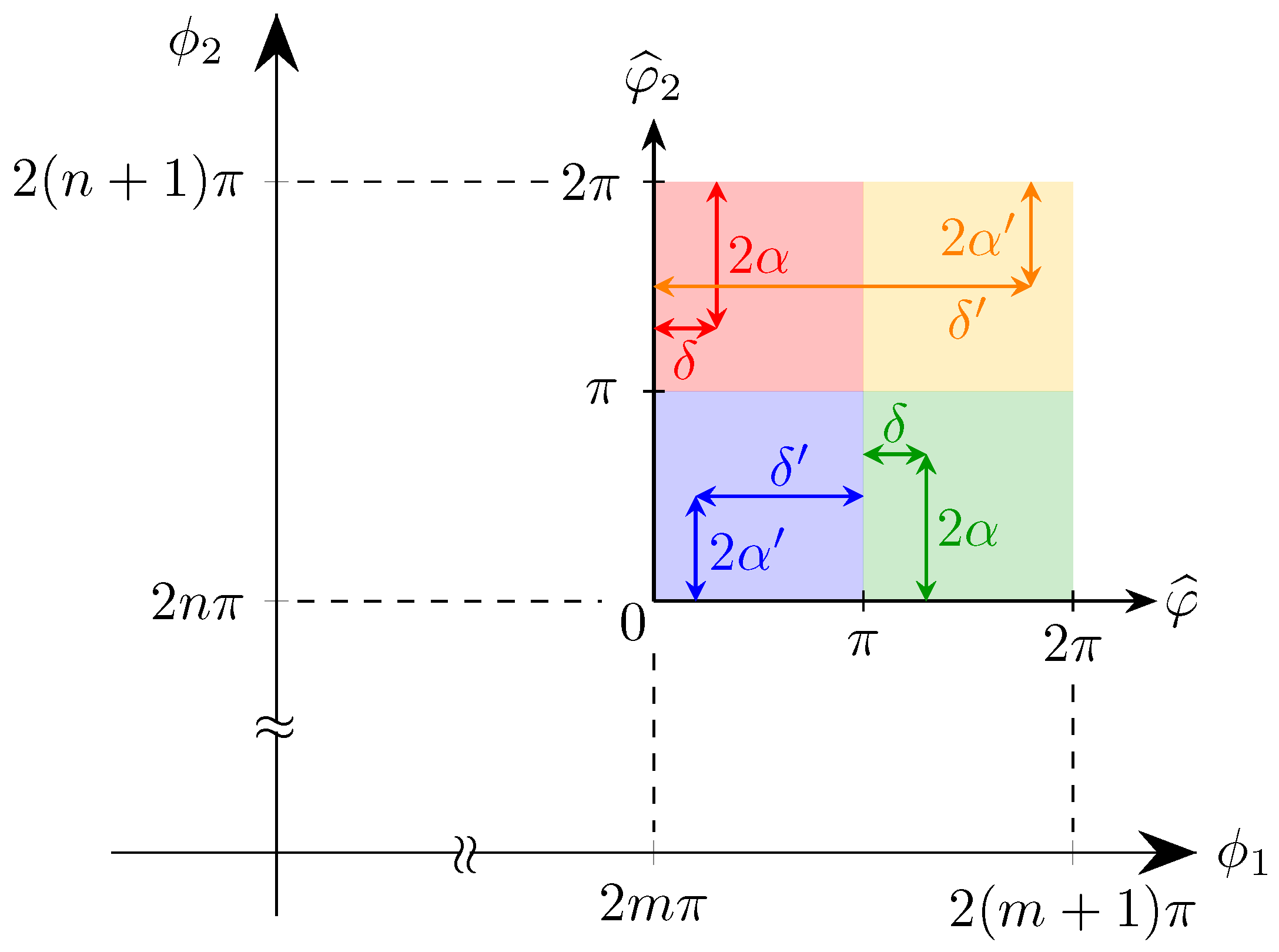
Figure 10.
Diagram for the determination of the input SOP: and are the actual applied phase shifts, whereas and are the remainders; the new origin is placed in . The top quadrants (shaded in red and yellow) correspond to the first solution, , while the lower ones (blue and green) to the second solution. Polarisations with the same value of lie in diametrically opposed quadrants: the red and green concern the case of , whilst the yellow and blue ones to .
Figure 11.
Schematic of the integrated polarisation controller. The labels are as in
Figure 1.
Figure 11.
Schematic of the integrated polarisation controller. The labels are as in
Figure 1.
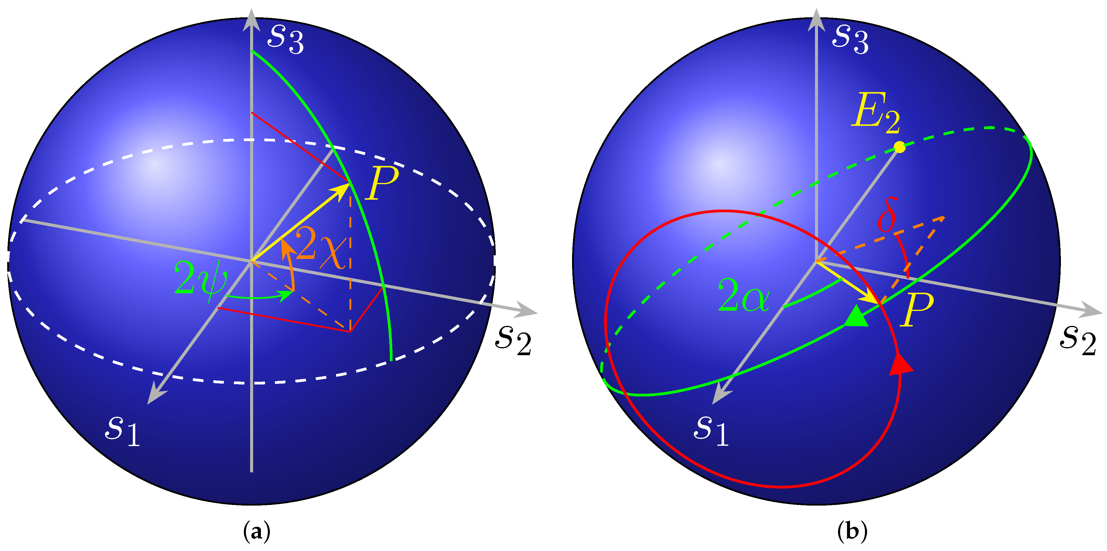
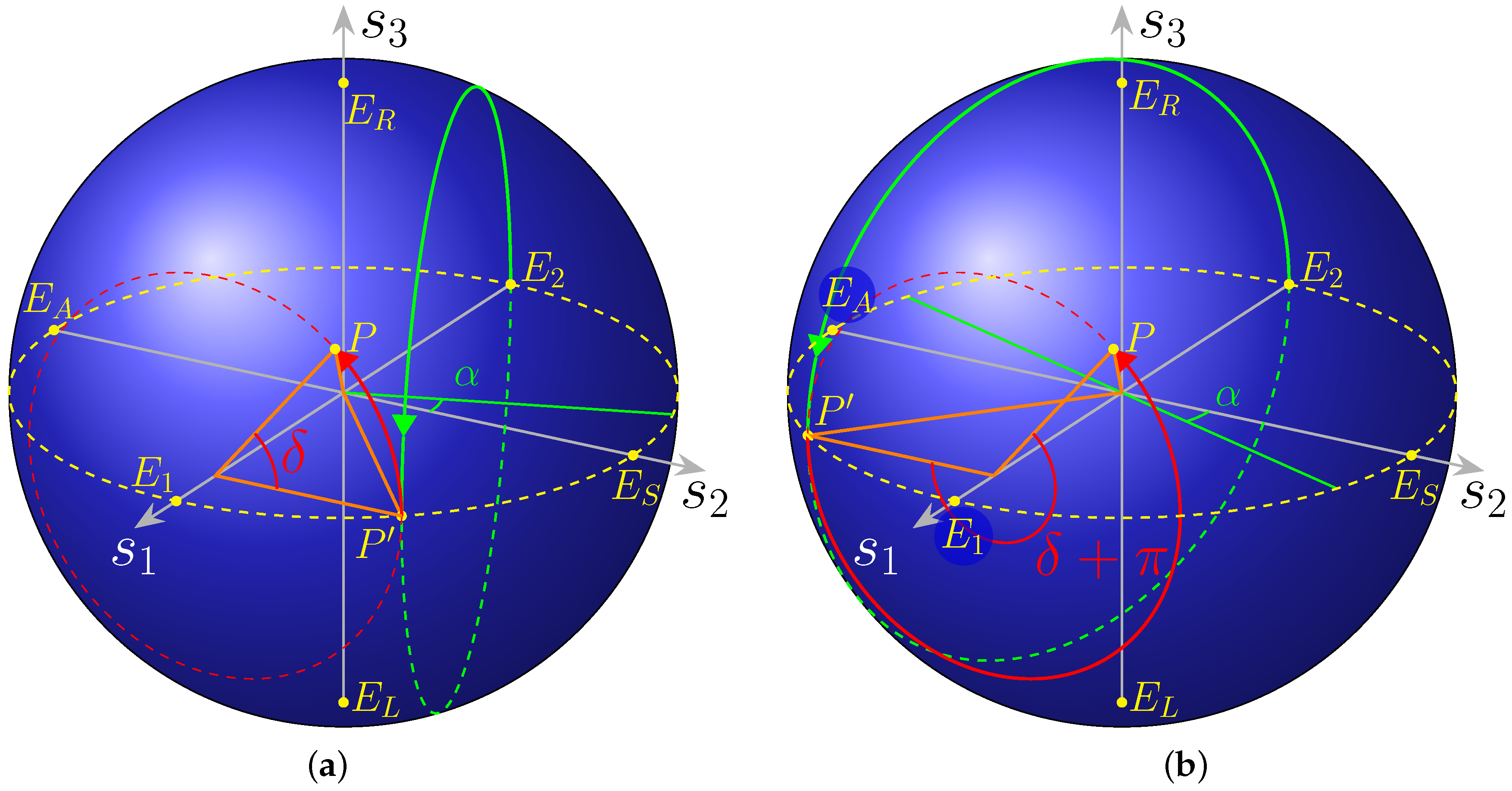
Figure 12.
Poincaré sphere. (a) Any SOP can be represented by a point P on its surface, by Equation (42). The usual spherical coordinates are used. (b) Poincaré sphere with the angles as in Equation (41). The point P corresponds to a generic polarisation state. The red and green circles display the trajectory on the sphere when a complete sweep is performed on the angle () and (), respectively, while the other is held constant. Notice the direction of the arrows on the circles: scanning on results in a counterclockwise rotation, whereas the opposite happens for , as the phase shifter is assumed to be in the lower arm.
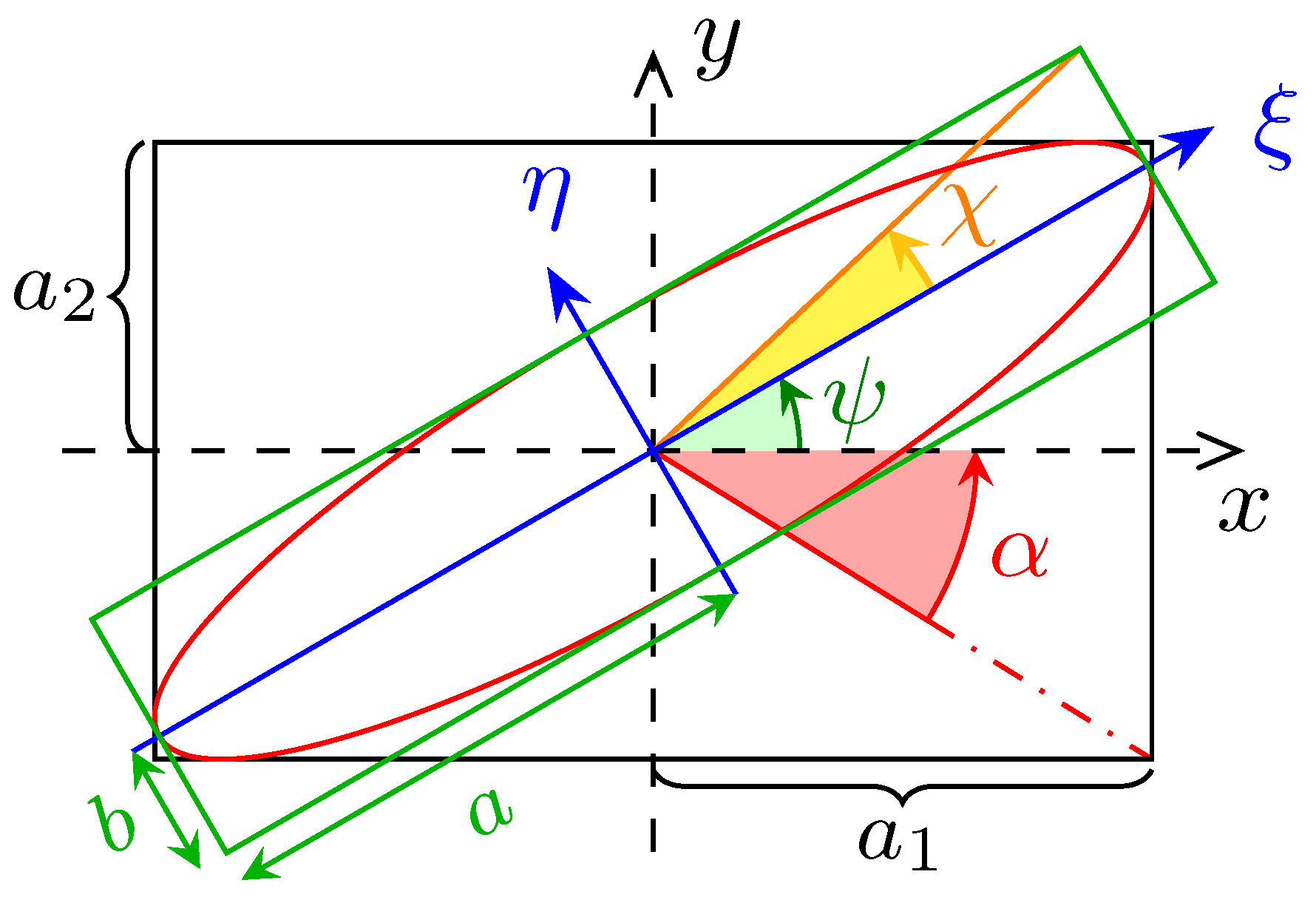
Figure 13.
Elliptically polarised wave seen in the observer () and in the ellipse () frame. The vibrational ellipse is for the electric field. The semi-major axis is tilted from x by the angle . The semi- axes length are a and b, not to be confused with the amplitudes and of the oscillations expressed in .
Figure 14.
Action on SOP of the circuit, seen as a MZI followed by a phase shifter, for , in the case of (a) the first solution set; and (b) the second solution set.
Figure 14.
Action on SOP of the circuit, seen as a MZI followed by a phase shifter, for , in the case of (a) the first solution set; and (b) the second solution set.
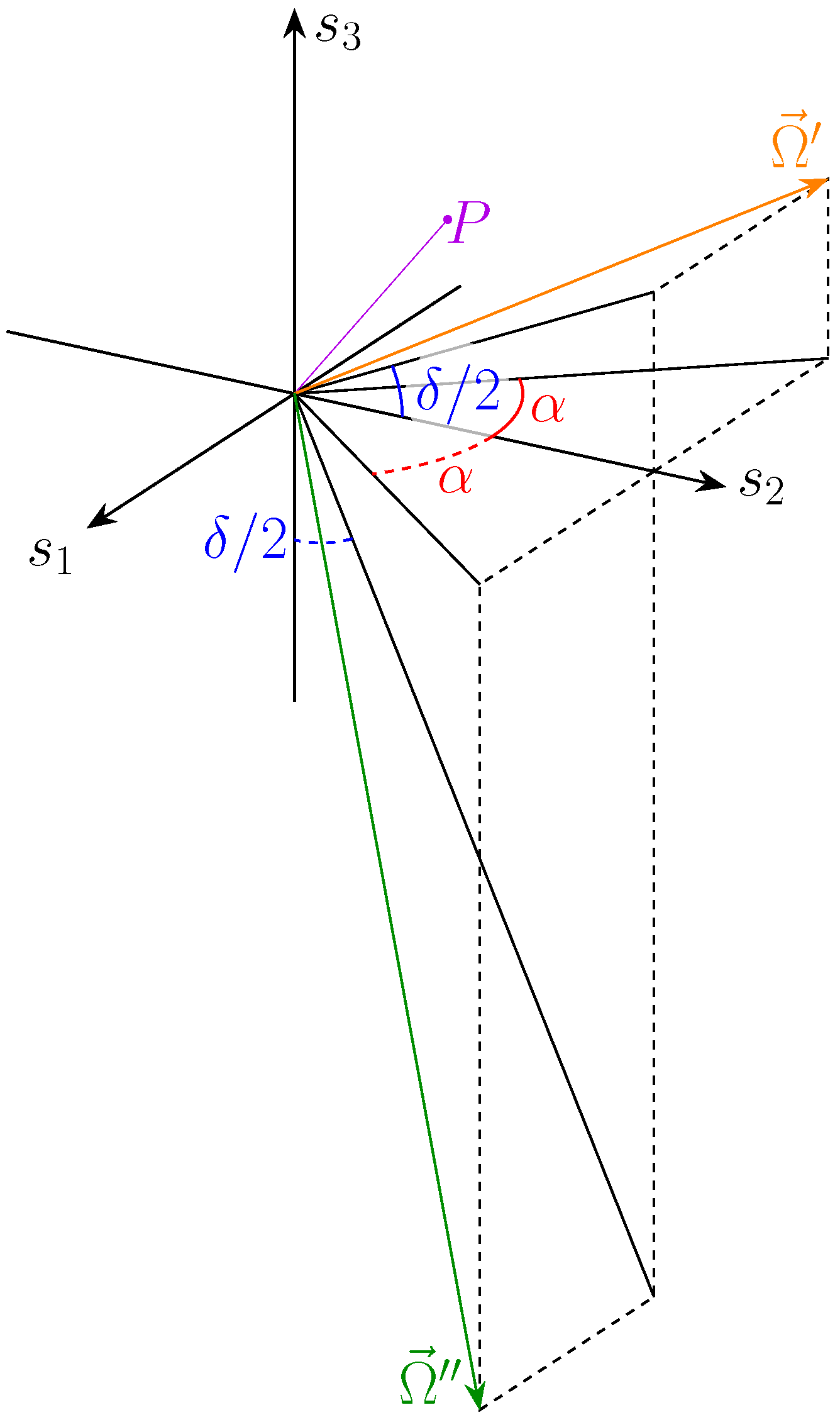
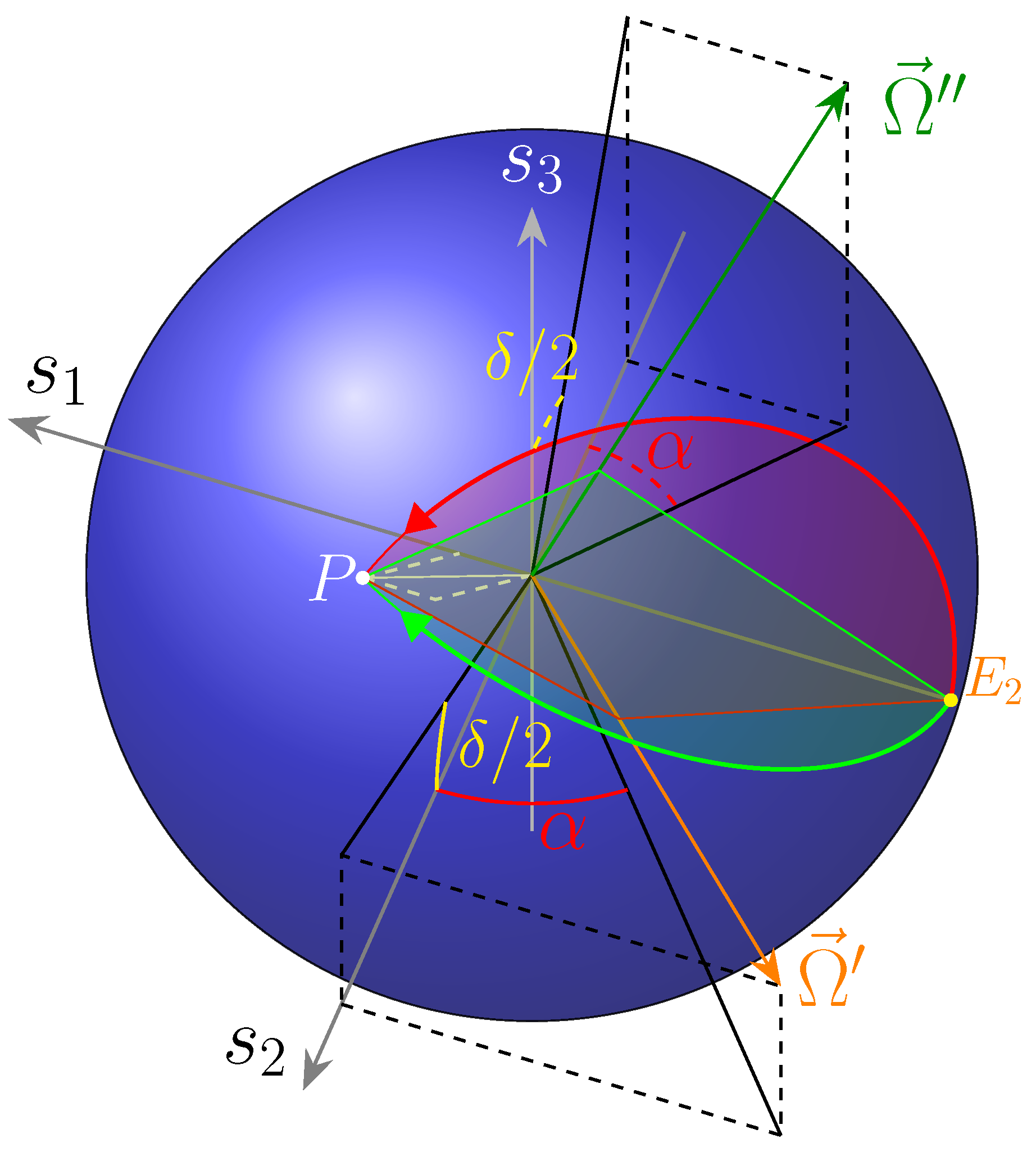
Figure 15.
Rotation axes for the two solution sets.
Figure 15.
Rotation axes for the two solution sets.
Figure 16.
Overall device effect, for the two solutions.
Figure 16.
Overall device effect, for the two solutions.
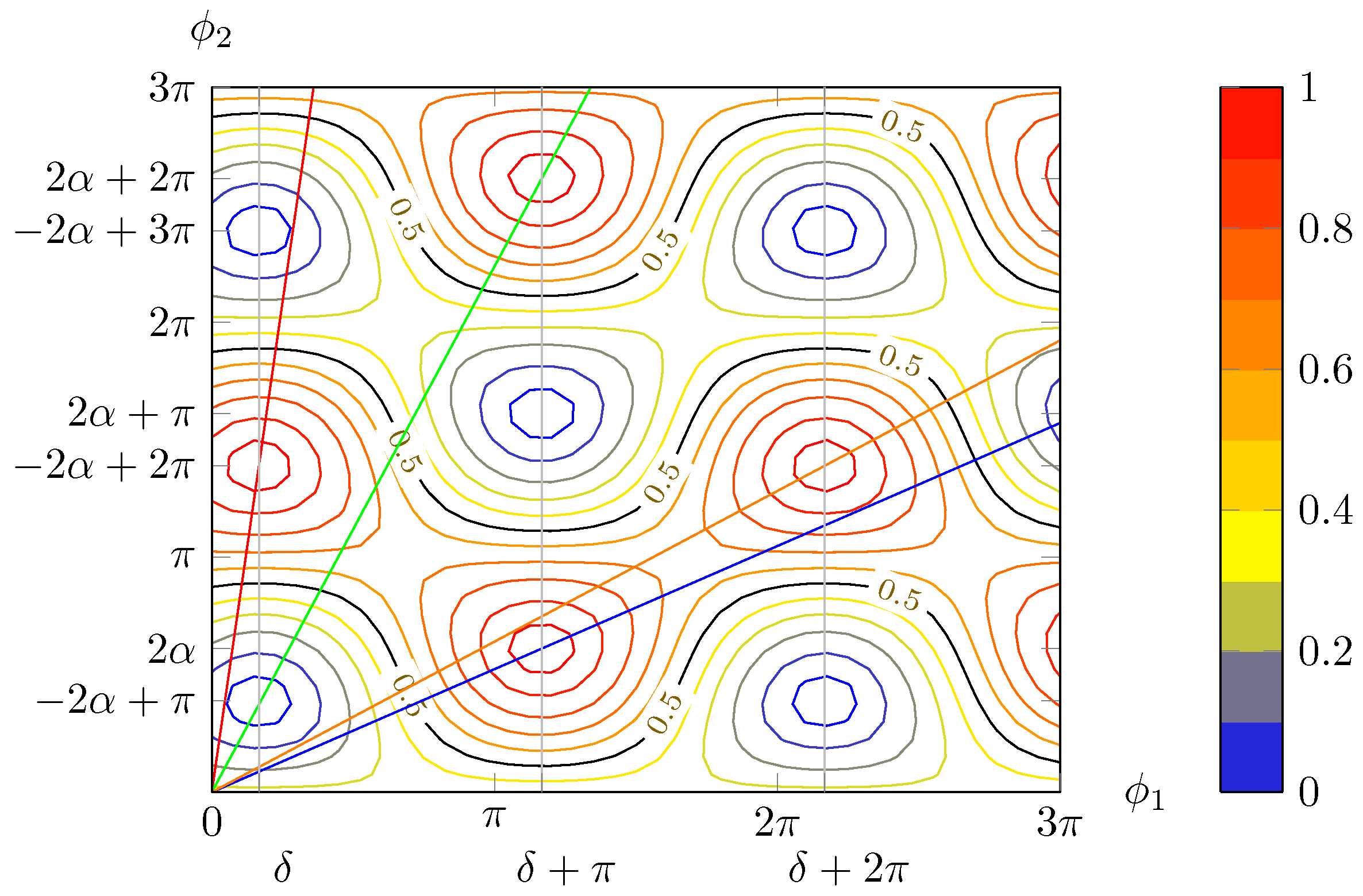
Figure 17.
The pair of phase shifts as a function of frequency are lines (in different colours for each solution, refer to the legend of
Figure 18) passing by the origin and the chosen peak, in the plane
. For comparison, the contour plots for
and
° are included. Note that those lines in general do not pass through other maxima.
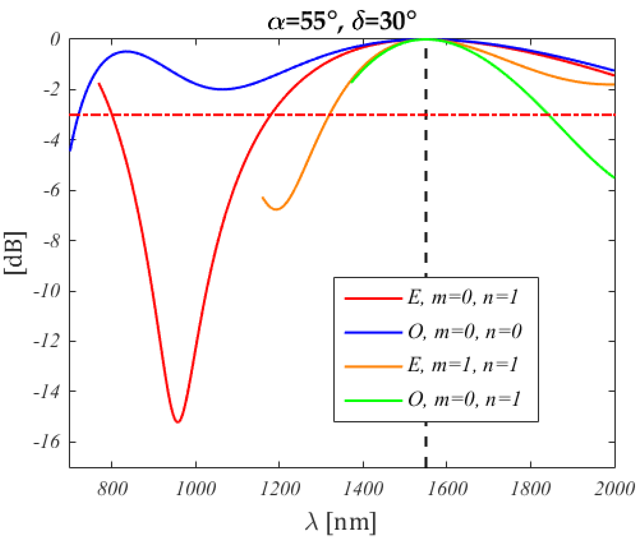
Figure 18.
Spectra corresponding to the lines in
Figure 17 (the colours correspond), for
1934
(1550
, indicated by the black dashed vertical line). The wavelength ranges have been chosen to represent only the portion of the
plane shown in
Figure 17. Note that the upper wavelength limit is the same, whereas the lower one increases with the solution distance from the origin. In general, the spectra are neither symmetric nor periodic. The legend lists the solution class (even or odd) and their order. The fundamental even solution is not reported, as it lies in the lower
half plane.
Figure 19.
Family of Clélie curves, in the (a) direct form (Equation (91)), for the parameter ranging from to 3, at steps of 1/9. Note that curves with different values of the parameter may pass by the same point, corresponding to different order solutions that have a different frequency behaviour. (b) The inverse form (Equation (95)), for the same parameter values of (a), in growing order from red to violet. The equator, in yellow, corresponds to , while in the previous figure it corresponds to .
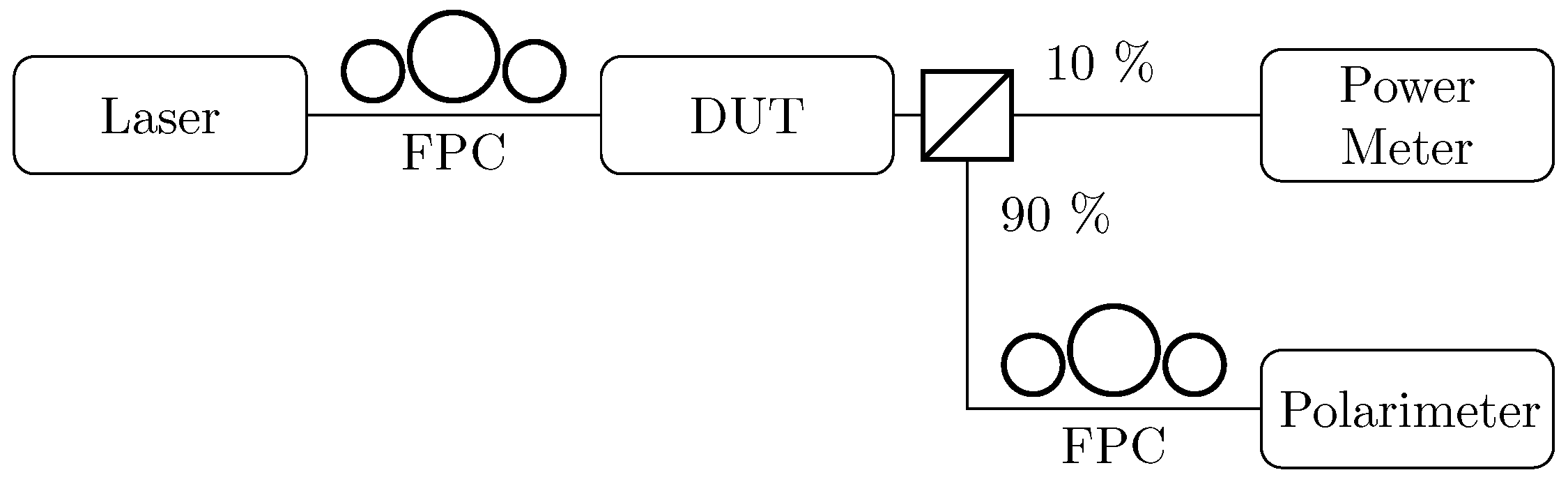
Figure 20.
Setup used for the characterisation of the controller configuration. FPC, fibre polarisation controller; DUT, device under test.
Figure 20.
Setup used for the characterisation of the controller configuration. FPC, fibre polarisation controller; DUT, device under test.
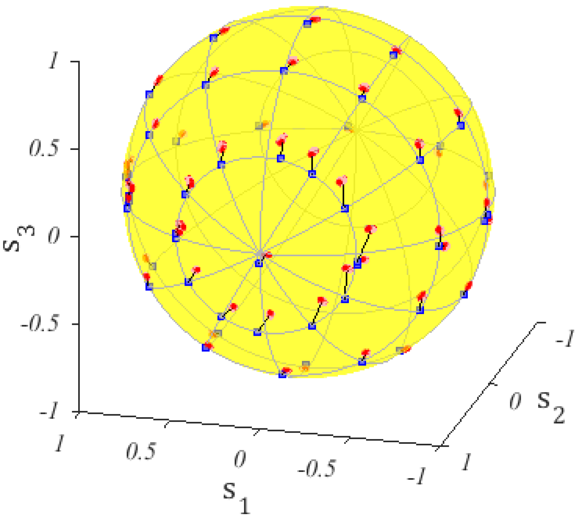
Figure 21.
Comparison between experimental data points as read on the polarimeter (blue squares) and as deduced from the dissipated power on each heater (red), measured by the sourcemeter and correcting the effect of the parasitic common ground electrode resistance. The start point for and is that with . Increasing produces a counter clockwise rotation around the axis, on the axis, when .
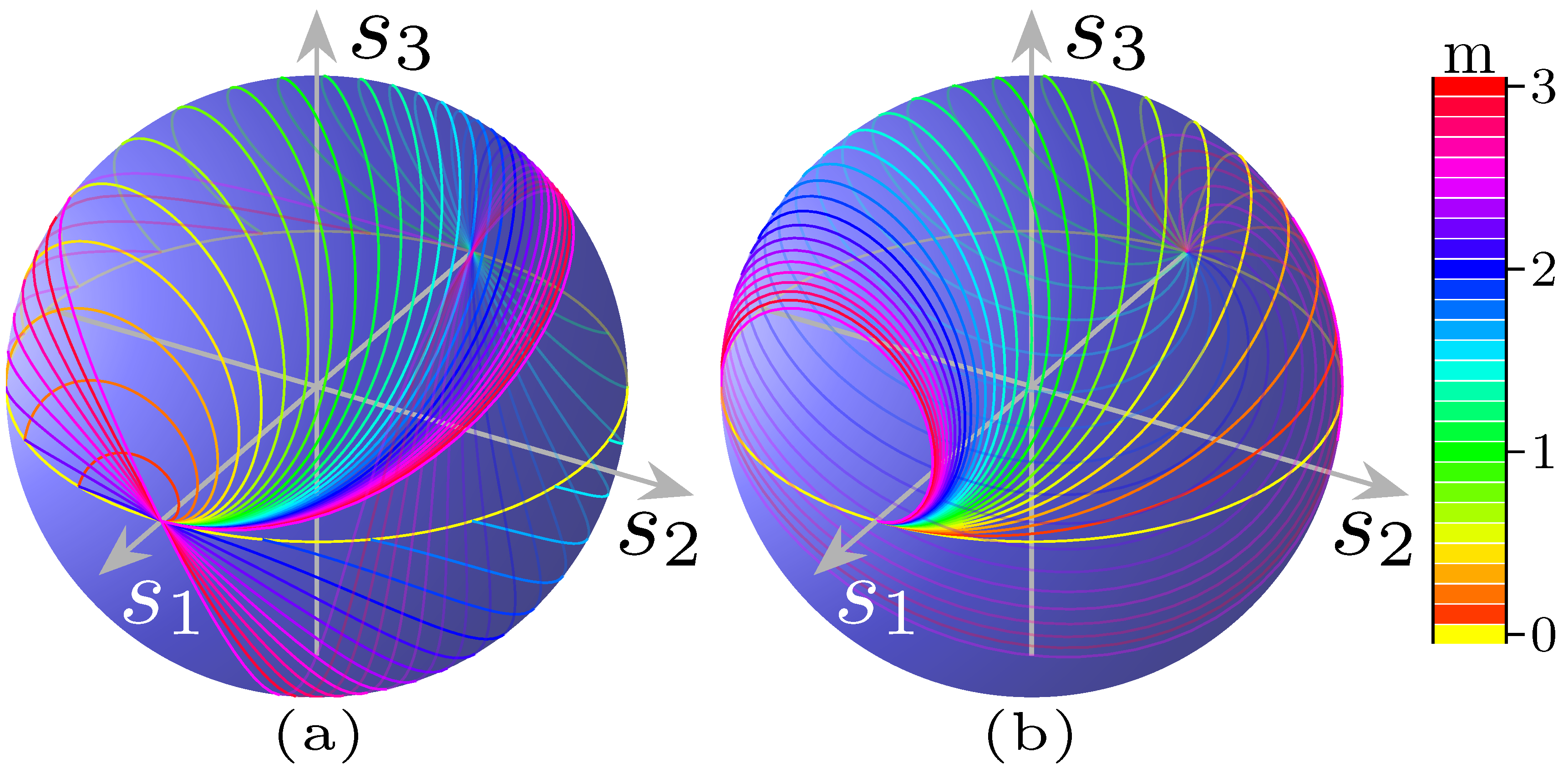
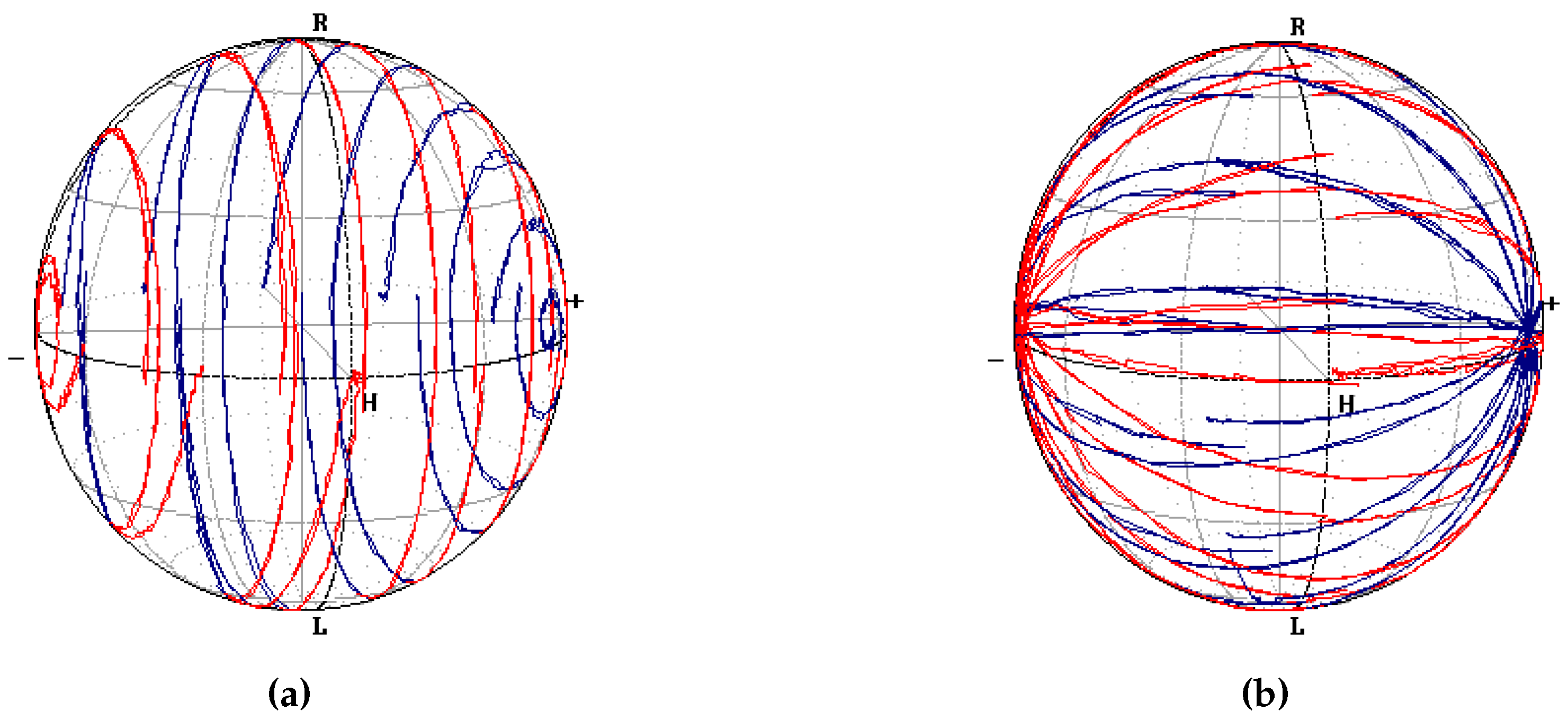
Figure 22.
Curves traced on the polarimeter when scanning on (
a)
and (
b)
, while keeping the other phase constant. The polarimeter has been calibrated so that the SOP from the SPGC is shown as a 45° linear polarisation. Red curves lie on the hemisphere on the observer’s side, blue ones on the rear one. The axes are rotated by 90° around
, with respect to
Figure 21.

 ,
, 