Review

Isolated DC-DC Power Converters for Simultaneous Charging of Electric Vehicle Batteries: Research Review, Design, High-Frequency Transformer Testing, Power Quality Concerns, and Future

by
Srinath Belakavadi Sudarshan
and
Gopal Arunkumar
*
School of Electrical Engineering, Vellore Institute of Technology, Vellore 632014, India
*
Author to whom correspondence should be addressed.
Sustainability 2023, 15(3), 2813; https://doi.org/10.3390/su15032813
Submission received: 21 December 2022 / Revised: 28 January 2023 / Accepted: 30 January 2023 / Published: 3 February 2023

Abstract

:
The transportation industry is transitioning from conventional Internal Combustion Engine Vehicles (ICVs) to Electric Vehicles (EVs) due to the depletion of fossil fuels and the rise in non-traditional energy sources. EVs are emerging as the new leaders in the industry. Some essential requirements necessary for the widespread adoption of EVs include sufficient charging stations with numerous chargers, less to no wait time before charging, quick charging, and better range. To enable a quicker transition from ICVs to EVs, commercial organizations and governments would have to put in a mammoth effort, given the low number of installed chargers in developing nations such as India. One solution to lower the waiting time is to have multiple vehicles charging simultaneously, which might involve charging two- and four-wheelers simultaneously, even though their battery voltage ratings differ. This paper begins by providing the details of the power sources for EV charging, the charging levels and connector types, along with the specifications of some of the commercial chargers. The necessity of AC-DC converters in EV charging systems is addressed along with the power quality concerns due to the increased penetration of EVs. Next, a review of the existing research and technology of isolated DC-DC converters for simultaneous charging of EV batteries is provided. Further, several potential isolated DC-DC converter topologies for simultaneous charging are described with their design and loss estimation. A summary of the existing products and projects with simultaneous charging features is provided. Finally, insight is given into the future of simultaneous charging.

1. Introduction

The primary mode of transportation in the world is petrol- and diesel-based vehicles. These vehicles use internal combustion engines (ICEs) to burn the fuel to run the vehicle. However, there are several issues with the use of ICEs. It has low fuel efficiency, higher operating cost, and harmful emissions [1]. Due to the emissions of ICEs, the resultant climate changes have led to the development of hybrid electric vehicles (HEVs) and electric vehicles (EVs).

1.1. Methods of Obtaining Electricity for Charging

Conventionally, electricity is obtained from thermal, hydro, and nuclear power plants. While fossil-fuel-based thermal power plants can be used to produce power in mega-watt levels, they also produce harmful gases such as carbon dioxide, carbon monoxide, sulphur dioxide, nitrogen oxide, and ash [2], which has led to a steady increase in the global temperature [3], and which in turn has caused the degradation of flora and fauna, and the health of humans. In addition, the depletion of fossil fuels is a significant threat to the continued use of fossil fuel-based power generation. The connection between emissions and fossil fuel depletion is a significant concern today [4]. While hydro plants do not lead to such an issue, the main problems with the hydro plant are related to the submergence of the areas surrounding the dam, the impact on the water resources, and the rainfall amount. The impact depends mainly on the dimensions of the hydro plant [5]. With nuclear power plants, the main issue is related to resource availability, the complexity of control, the potential risk of leakage, and waste disposal. Various nations have developed several policies to prevent nuclear disasters [6]. To prevent the issues resulting from the conventional sources, non-conventional energy sources have been introduced into the power generation sector. Among these resources, the solar photovoltaic (PV) system is being used due to abundant resource availability. Since solar panels can be integrated with vehicles, solar PV is an attractive option as a source to charge EVs. Nasr et al. [7] have comprehensively reviewed solar PV based converters for EV battery charging. Several non-isolated converters suitable for EV battery charging have been reviewed, along with gird integrated converters. The primary issue that needs to be addressed with the use of PV systems is the intermittency and variations of solar irradiance and temperature. The intermittency has been addressed by Jin et al. [8]. Energy optimization is necessary with the use of PV systems, as addressed by Al-Shahri et al. [9].
EVs, specifically battery electric vehicles (BEVs), have contributed to reducing pollution as they create no gas emissions. However, an important point to note is the power source for charging [10]. If coal-based power plants are used for power production to charge the battery, the burden on the system will be dominant. The positive environmental impact will be significantly higher when renewable energy resources are used [10]. Another issue that needs to be focused on with the increased use of EVs is the recycling and disposal of a battery that has been damaged or completed its life cycle. Yu et al. [11] have addressed the challenges in recycling Li-ion batteries and provided several suggestions to address recycling. If these issues are addressed effectively, the use of EVs can create a more positive impact on the environment.
EV research is experiencing a boom in the present day due to a renewed emphasis on reducing our carbon footprint [12], greenhouse gas emissions, and the depletion of fossil fuel resources. Several significant difficulties have gained attention due to the growing interest in EV use. These problems include, but are not limited to, the following:
  • Power quality concerns due to EV charging;
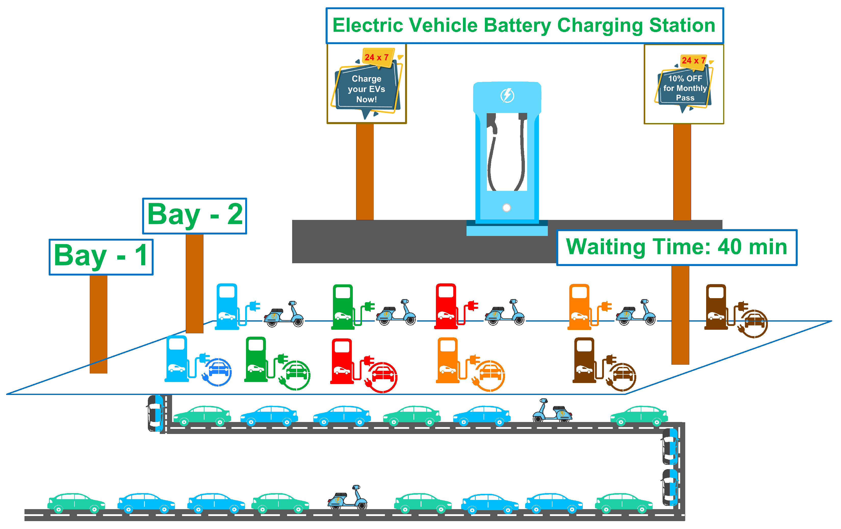
  • Low number of charging stations;
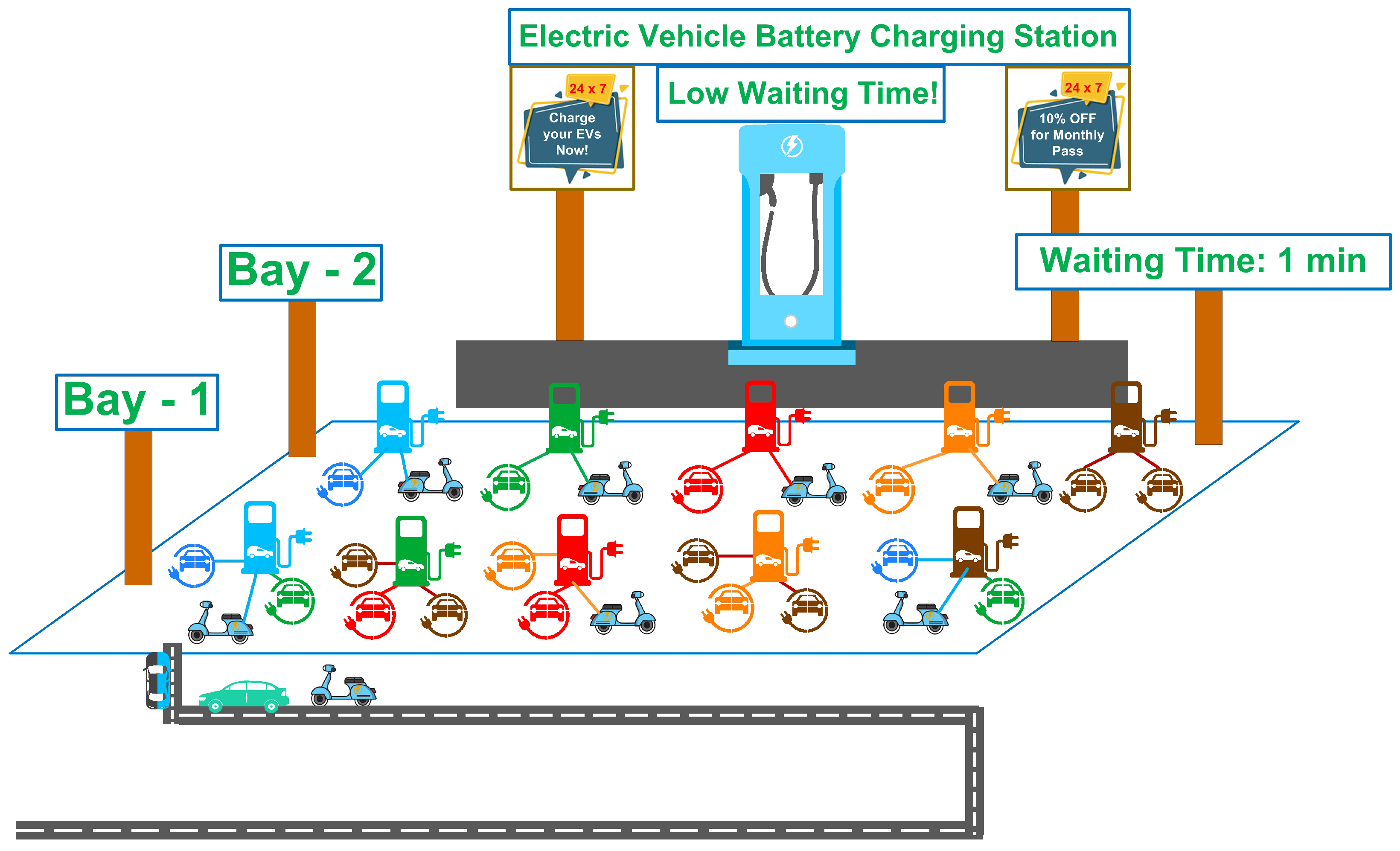
  • Long waiting time before charging;
  • Higher time for charging;
  • Lower range of EVs.
Government policies outside the research community’s purview influence the number of charging stations. The EV range issue is related to the type, C-rate, and battery rating, which the battery manufacturers and researchers of battery technology usually address. Electrical engineering research is directly or indirectly interested in the challenges of power quality issues and reducing the waiting and charging times.

1.2. Charging Techniques for EV Batteries

The technology or method employed for charging depends on the battery chemistry. Generally, Lithium-ion (Li-ion) batteries are used in EVs due to their high energy density, longer lifetime, and good electrochemical properties [13]. Several techniques for charging EV batteries have been recommended and reviewed by researchers for EVs. Shahjalal et al. [14] have provided the details of the various charging techniques for EV batteries. The charging methods could be conventional (slow) charging or fast charging. Conventional charging methods include constant current (CC) charging, constant voltage (CV) charging, and constant-current constant-voltage (CC-CV) charging. Several researchers have investigated the idea of reducing charging time by employing fast charging methods [15] such as flash charging [16], pulse charging [17,18], negative pulse charging [19], multistage current control protocol [20], variable current profile charging [21], boost charging [22], and other algorithm-based methods [23,24]. Hemavathi et al. [25] have provided details of the various conventional and fast charging methods with a qualitative comparison. In addition, the battery modeling has been provided with charging methodologies specific to various converters. Different charging levels have been described, along with the charging station architectures and fast charging topologies. The future trend of EV charging has been described to include smart charging, integration of renewable sources, wireless charging, and battery swapping. The authors have provided the road map of EV adaption. Research focus has also been shifted to address the degradation effects on the battery due to fast charging [26,27,28], its effect on the existing grid [29,30,31], and possible solutions [32]. While several of these methods are still at the research level, implementation in real-world EVs is a possibility that needs to be addressed by the research and development wing of the manufacturers.

1.3. EV Charging Levels, Connectors, and Standards

The charging levels are based on the power supplied, the source, and the charging time [25,33].
  • Level-1 charging, also known as AC charging or residential charging, can supply up to 2 kW power from a 120 V, 16 A single-phase source;
  • Level-2 charging, also known as AC split-phase charging, can supply up to 20 kW power from a 240 V, 80 A single-phase/split-phase source;
  • Level-3 charging, also known as DC charging, can supply between 120 kW and 350 kW power from a variable DC source between voltages of 200 V and 920 V, at a maximum current of 500 A;
  • Level-4 charging or Tesla Charging can supply 120 to 250 kW power from a 120 or 240, or 400 V source. This is applicable only for Tesla EVs.
A level-1 charger will require around 17–20 h to fully charge a battery with a 2 kW rating, while a level-2 charger will fully charge a 6.6 kW rated battery within 3.5 h. Level-3 and level-4 chargers are fast chargers that can charge high-power batteries in under 30 min [25,33]. The Electric Vehicle Supply Equipment (EVSE) for EVs and plug-in hybrid vehicles (PHEVs) are governed by IEC 61851-1:2017 standards for the conductive charging system. For India, Bharat EV standards have been proposed by the Government of India to standardize EV charging in the country. Kumar et al. [34] have reviewed India’s EV charging station standards. The authors have presented the present scenario of EVs in India and the different charging levels with the connector specifications. The authors have also presented the details of the various existing international standards with their applications. Details of Indian Standards (IS) have been described in detail with the charging methodologies (CHArge de Move (CHAdeMO), Combined Charging System (CCS), and Tesla.). Based on the charging standard, the types of connectors have been standardized. The specifications of such charging connectors are listed below:
  • AC Connector [25]
    • Type-1: up to 7.4 kW; follows SAE J1772 standard;
    • Type-2: up to 43 kW for public charging; follows IEC 62196-2 standard.
  • CHAdeMO [25,35]
    • Present: 50 kW, 500 V/125 A rated high power charger;
    • Proposed: over 100 kW, 500 V/200 A rated high power charger;
    • ChaoJi (CHAdeMO 3.0): over 500 kW, 600 A rated high power charger for fast charging.
  • CCS [25,36]
    • Type-1: 90 kW, 600 V/150 A (maximum ratings); 13 kW, 250 V (nominal rating);
    • Type-2: 170 kW, 850 V/200 A (maximum ratings); 44 kW, 230 V (single-phase)/ 440 V (three-phase) (nominal rating);
    • Type-2 and DC connector Combination: 43 kW for AC charging and 100 kW for DC charging; can go up to 350 kW.
  • Tesla Supercharger [25]
    • 480 V fast charging technology.
The newer definitions/ratings of chargers are proposed to enable fast charging and are suitable for high-power vehicles.

2. Commercial EV Charger Specifications: Present Market Status

Several commercial organizations have their own patented EV charging stations with specific advantages and features for the benefit of the customers. Some companies have provided their charger specifications to help the public understand their charging system specifications to enable an informed choice. This section gives a list of some of the electrical specifications of the chargers.

2.1. Eaton Corporation

2.1.1. AC Charger-Eaton xChargeIn Mobility

The specifications of the Eaton AC Charger-Eaton xChargeIn Mobility are listed below [37].
  • Power Range: 3.7 kW to 22 kW;
  • Connector Type: Type 1 for power levels up to 7.4 kW, and Type 2 for power levels up to 22 kW;
  • Input Voltage: 230 V, 50 Hz (1-phase) and 400 V 50 Hz (3-phase);
  • Input Current: 16 A and 32 A for both 1-phase and 3-phase at respective power levels;
  • Simultaneous Charging: No (only one vehicle can be charged at any given time).

2.1.2. DC Charger-Green Motion DC 22

The specifications of the DC Charger-Green Motion DC 22 are listed below [38].
  • Power: 22 kW;
  • Input Voltage: 400 V 50 Hz (3-phase);
  • Power Factor: Greater than 0.99;
  • Input Current: 32 A;
  • Output Voltage Range: 50 to 500 V DC;
  • Output Current: 55 A;
  • Efficiency: Greater than 96%;
  • Simultaneous Charging: No (only one vehicle can be charged at any given time).

2.1.3. DC Charger-Green Motion DC 44

The specifications of the Eaton DC Charger-Green Motion DC 44 are listed below [39].
  • Power: 44 kW;
  • Input Voltage: 400 V 50 Hz (3-phase);
  • Power Factor: Greater than 0.99;
  • Input Current: 64 A;
  • Output Voltage Range: 50 to 500 V DC;
  • Output Current: 110 A;
  • Efficiency: Greater than 96%;
  • Simultaneous Charging: No (only one vehicle can be charged at any given time).

2.1.4. DC Charger-Green Motion DC 66

The specifications of the Eaton DC Charger-Green Motion DC 66 are listed below [39].
  • Power: 66 kW;
  • Input Voltage: 400 V 50 Hz (3-phase);
  • Power Factor: Greater than 0.99;
  • Input Current: 96 A;
  • Output Voltage Range: 50 to 500 V DC;
  • Output Current: 165 A;
  • Efficiency: Greater than 96%;
  • Simultaneous Charging: No (only one vehicle can be charged at any given time).

2.2. Siemens

2.2.1. SICHARGE D for DC Fast Charging

The specifications of the Siemens SICHARGE D are listed below [40].
  • Nominal AC Input Voltage: 400 V, 50/60 Hz;
  • Nominal Input Current: 301 to 515 A, based on output power;
  • Power Factor: Greater than 0.99 at full load;
  • DC Output Power: 160 to 300 kW;
  • DC Output Voltage: 150 V to 1 kV.

2.2.2. VersiCharge for AC Charging

The specifications of the Siemens VersiCharge are listed below [41].
  • Nominal AC Input Voltage: 230 V (1-phase), 230 or 400 V (3-phase); 50/60 Hz;
  • Nominal Input Current: 10 to 32 A, based on output power;
  • DC Output Power: up to 7.4 kW (1-phase), up to 22 kW (3-phase);
  • DC Output Current: 32 A maximum.

2.3. Need for Simultaneous Charging of EV Batteries

A significant issue that needs to be addressed is the reduction in waiting time before charging. One of the ways to reduce this is by installing more charging stations. While this process can reduce the waiting time before charging, installing more charging stations is related to other variables, such as land availability and acquisition and availability of power supply. Increasing the number of charging stations may not be a very simple or practical solution. In addition to optimizing the number of charging stations, it would be of great help if simultaneous charging of multiple EVs with the same or different rating batteries could be implemented. In a scenario where there are 10 chargers in a charging station, with each charger capable of charging 1 EV at a time, 10 EVs can be charged at any given time. This is shown in Figure 1. If it is possible to charge more than 1 battery (say, 2) in 1 charger, then the charging station described above can charge 20 EVs simultaneously. This creates a significant reduction in waiting time. This will directly create a positive impact on the conversion from ICEVs to EVs for mass-use. An added advantage will be obtained if multiple EVs of different ratings (say, an electric-bike and an electric-car) can simultaneously be charged by the same charger. This is shown in Figure 2. In addition to reducing waiting time, simultaneous charging also leads to higher profit for the company that installs and maintains the charging station since more vehicles can be charged in a given time-period, leading to an overall increase in the number of vehicles that are being charged each day. With this, we can conclude that simultaneously charging multiple batteries of the same and different ratings offers many advantages to customers and companies.
Several authors have provided a detailed review of the various converters that can be used for EV battery charging. Khalid et al. [42] have reviewed the various isolated and non-isolated converter configurations that suit EV battery charging. In addition, the authors have provided the configuration of a charging station for fast charging, which includes the AC-DC multilevel converters. The concept of universal chargers has been described in work with various charging methods. However, the work does not deal with simultaneous charging and the corresponding modifications in the converters. In addition, the required design equations and loss calculation are beyond the scope of the review. Ghasemi-Marzbali et al. [43] have dealt explicitly with the infrastructure for fast charging of electric vehicles. The work gives details of the studies required for the charging station design, site selection and size determination, charging time estimation, and modeling of renewable energy resources for charging stations. The demand-side management principle has been introduced with risk factors and reliability considerations. The application of machine learning for system design has been described with a particular focus on fast charging stations. However, the work does not describe any converter topology required in the charger since the work’s objective is to review fast charging station requirements. Chakraborty et al. [44] have reviewed the various DC-DC converter topologies with a special focus on EV battery charging. Several isolated and non-isolated DC-DC converter topologies have been described in the work. Under the isolated converter topologies, full-bridge, current-fed converter, sinusoidal amplitude high voltage bus converter, and multi-input single output converters have been described. Design formulae for the memory elements have been provided for the described converters. The architecture of fast charging stations has been provided with a description of converters for the AC-DC and DC-DC conversion stages. In the DC-DC stage, full-bridge and phase-shifted full-bridge topologies for single-battery charging have been described. Common equations for loss estimation have been provided with the comparative efficiency for various switching frequencies. Various performance parameters have been compared for the described converters. However, the work does not describe loss estimation specific to the converters and does not include details for simultaneous charging. In addition, only some isolated converters have been described in previous work.
This work presents a detailed description of the various isolated converters that can simultaneously charge multiple EV batteries. While high-power converters such as full-bridge and its derived converters can be used to charge the battery of any vehicle, it is essential to note that a converter will give the desired performance only when it is operated at or close to the rated or designed conditions [45]. For example, a full-bridge converter-based charger designed for 10 kW can charge an electric car and an electric bike of low rating (say 250 W, such as the Hero Electric Flash electric bike used in India). However, not only will the converter be underutilized to deliver very low power for charging the electric bike, the cost per unit will be high when operated at low power [45]. To avoid this problem, isolated converters that can deliver low and medium-range power are very much needed when simultaneous charging infrastructure is planned since the same charger module should be able to charge vehicles with diverse power ratings. Thus, it is necessary to consider low and medium-power range isolated converters for EV battery charging applications, especially with simultaneous charging. This work also presents the detailed design and loss estimation process for various converters for low, medium, and high-power charging. In addition, a procedure for testing the high-frequency transformer (HFT) is provided, which has yet to be dealt with by previous literature.
This review work is organized as follows: Section 3 gives details of the main power quality issues that need to be addressed with battery charging. Section 4 details the various research works that have proposed and implemented simultaneous charging, with the advantages and limitations of each work. Section 5 explains the various isolated DC-DC converters that can be extended to charge multiple batteries simultaneously. The converters included in this section are the single-switch, two-switch isolated converters and bridge-type converters, including resonant converters, with their design equations and loss estimation. Section 6 gives a quantitative explanation of the multi-secondary HFTs required in the isolated converters for simultaneous charging with their testing procedure. Section 7 explains the trend of EV batteries shifting towards 400 V and 800 V levels. Section 8 describes the various products and projects that have implemented simultaneous charging features for public use. The paper concludes by describing the future research scope of simultaneous charging.

3. Power Quality Due to EV Charging: Concerns and Solutions

The supply systems in the world are invariably AC systems. This necessitates using an AC-DC converter in the battery-charging system. With grid connection, several important power quality parameters need to be considered. The power systems are usually designed keeping in mind the increase of load in the future. However, the sudden shift towards EVs has drastically increased the power demand, most likely more than the predicted demand. This has caused a negative impact on the grid and the system in general [46]. In addition, harmonics, low power factor, low voltage profile, and increased losses are causing significant trouble to the power system [46]. The power quality issues must be addressed more rigorously when multiple batteries are simultaneously charged. The power factor and the Total Harmonic Distortion (THD) are the most important parameters that must be addressed. IEC61000-3-2 [47] governs the Power factor correction (PFC) or harmonic reduction. These parameters will be controlled using a feedback control system designed for PFC and harmonic minimization.

3.1. Power Factor Correction

PFC can be done using two [48] methods: (a) passive PFC and (b) active PFC. The passive method uses passive components such as inductors and capacitors to filter out the harmonics. The passive method is suitable for low-power applications (less than 100 W) since it leads to lower efficiency, high cost, and weight due to the size of line-frequency inductors and capacitors. On the other hand, active PFC methods use switching regulators to correct the wave shape to obtain sinusoidal grid current at unity power factor. This method is complex but is suited for high power levels. Active PFC can be done using converters that operate in continuous conduction mode (CCM), critical conduction mode (CrCM), and discontinuous conduction mode (DCM).
The general requirements of a PFC AC-DC converter topology include a simple power stage with a low number of components, less distortions in the input current, and the ability to achieve a near-unity power factor. Kolar et al. [49] and Friedli et al. [50] have provided an exhaustive review of the various topologies of PFC rectifiers. Conventional Boost PFC Rectifiers (CBRs) operating in CCM are among the most popular PFC topologies [51]. Integrated PFC controllers such as NCP1650 by ON Semiconductors [52] also work as a CBR. With Silicon Carbide (SiC) and Gallium Nitride (GaN) MOSFETs and diodes, the issue of output diode reverse recovery is mitigated [53]. The design of the memory elements of the CBR is the same as that of a conventional boost converter. In addition to the CBR, dual boost bridge-less PFC rectifiers [54,55,56,57,58,59], totem-pole bridge-less PFC rectifiers [60,61,62,63], and interleaved boost PFC rectifiers [64] are more commonly used [65] in several products that need PFC. On the three-phase system side, Vienna rectifiers have become very popular [66] since they have inherent PFC capability. Several control techniques can be used to achieve a unity power factor. Examples of control strategies include hysteresis control [67,68], average and peak current mode controls [69,70,71,72,73], model predictive control [74], sliding controller [75], and one-cycle control [76,77].

3.2. Harmonics and THD

EV battery charging systems are made of multiple power electronic converters and analog electronic systems. These are non-linear loads to the grid and hence cause harmonics in the grid current. The harmonics will be very significant when multiple vehicles are being charged at the same time [78]. Not only will the harmonic pollution of the grid current be higher in that part of the power system, but it will also reflect on all its connected systems and cause distortion in those parts. The presence of harmonics affects the operation of all the connected equipment and can also cause failures with considerable financial implications. EV charging can cause unbalance in the power system. Due to the unbalance, negative sequence components can be produced, producing a second-order harmonic ripple in the DC link voltage. This causes distortions in the grid input currents. Equation (1) can be used to explain the effects of harmonics [79] on the DC-link. The presence of even-order harmonics on the DC-grid side will cause the generation of odd-harmonics on the grid-side, leading to power quality issues. In Equation (1), α represents the negative sequence components, and I d c represents the DC current.
V d c = 3 4 C I d c + I 2 4 π f s i n ( 4 π f t α 2 ) + I 4 8 π f s i n ( 8 π f t α 4 ) + I 6 12 π f s i n ( 12 π f t α 6 ) + I 8 16 π f s i n ( 16 π f t α 8 ) + I 12 24 π f s i n ( 24 π f t α 12 )
Other effects of harmonics on the various components of the power system are well known, and their solutions have been investigated for years. PFC converters are to be controlled such that the harmonics are mitigated well and the THD levels are within the permissible limits. In addition, strategic placement and optimal sizing of variable passive filters can also help in harmonic reduction. Alame et al. [80] have comprehensively analyzed the effects of harmonics due to EV charging on the various components of a distribution system. The authors have explained transformer loss modeling, temperature rise modeling, and lifetime modeling. A sample case study on a 1500 kVA distribution transformer has been provided to show that the percentage of harmonic currents increased with an increase in the battery state of charge. Further, the impact of EV charging on the distribution system has been analyzed by considering the IEEE 33-bus system charging four EVs at different buses using PV-based distributed generation units. The analysis has been performed using the decoupled harmonic power flow algorithm to obtain the effect on voltage quality and current THD. A centralized control flow has been proposed as an optimization problem to mitigate the effects of harmonics.

3.3. Other Detrimental Effects

Due to the diverse charging rates of EVs owing to slow, fast, and ultra-fast chargers, several negative effects can be observed. These include stability issues, unbalance, and overloading [79]. Dharmakeerthi et al. [81] have concluded that using fast charging stations can cause issues in the grid since they can significantly reduce the steady state voltage stability of the grid. In addition, the harmonics and inter-harmonics produced due to charging rates will also affect the power system’s critical components, such as transformers, breakers, cables, and meters. Alshareef and Morsi [82] have shown that fast charging stations can significantly affect and cause voltage flicker in distribution systems.
Despite these issues, EVs will be integral to our system since the advantages outweigh the limitations. Hence it is necessary to address these issues while designing a charging station. Nguyen et al. [78] have provided the topology of a photovoltaic inverter used as an active filter to mitigate power quality issues during simultaneous fast charging of five EV batteries. The proposed system models a bidirectional DC-DC converter acting as a charger and a DC-AC converter connected to the AC grid. Control structures for the control of both converters to implement harmonic mitigation have been explained, and the corresponding simulation results have been provided to validate the proposed scheme.
Once the AC power has been converted to DC and the power quality is maintained, a DC-DC converter is required to regulate the voltage, match the battery voltage level, and implement charging control. These DC-DC converters form a significant research area and are the focus of the following sections of this review, specific to the simultaneous charging of multiple batteries.

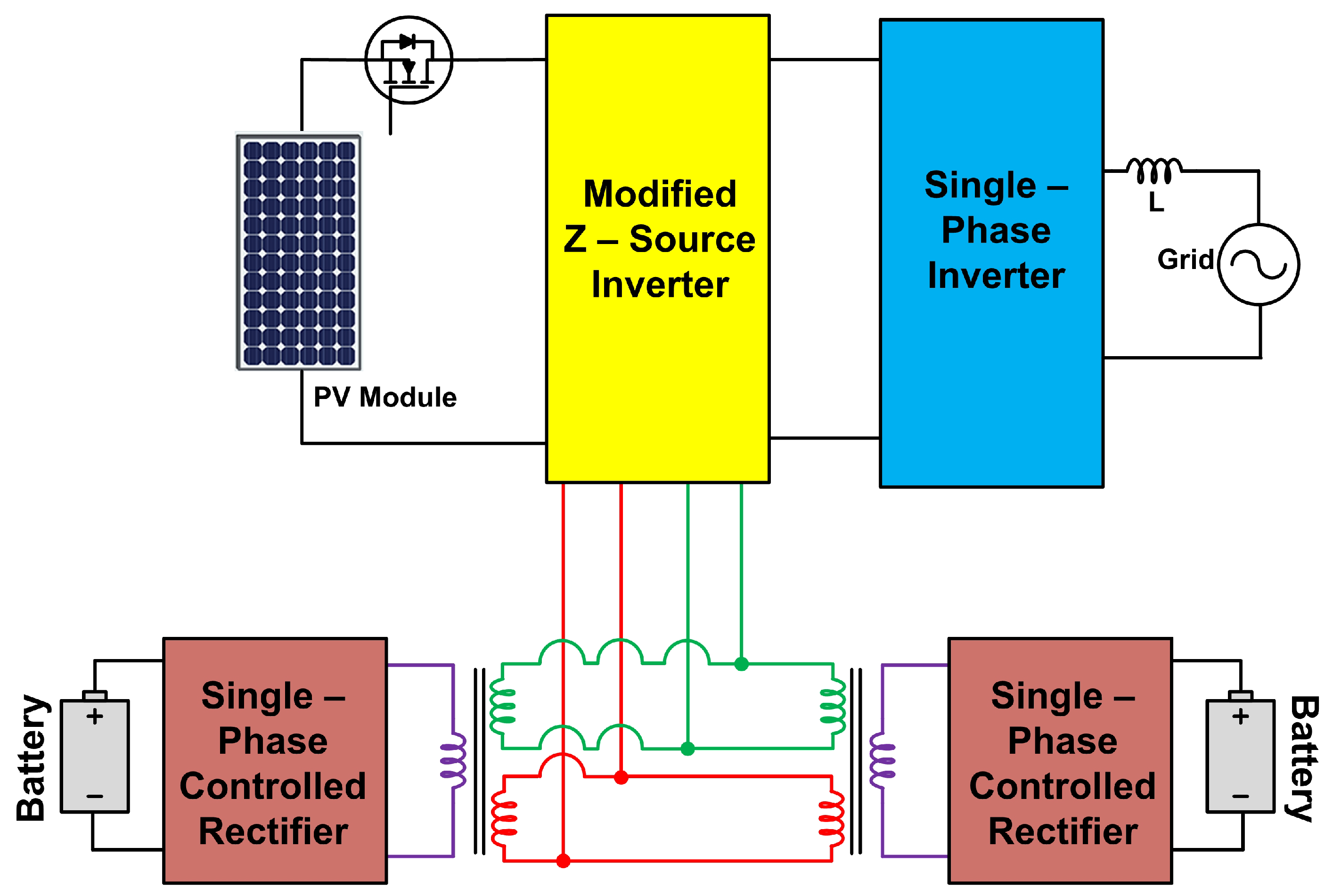
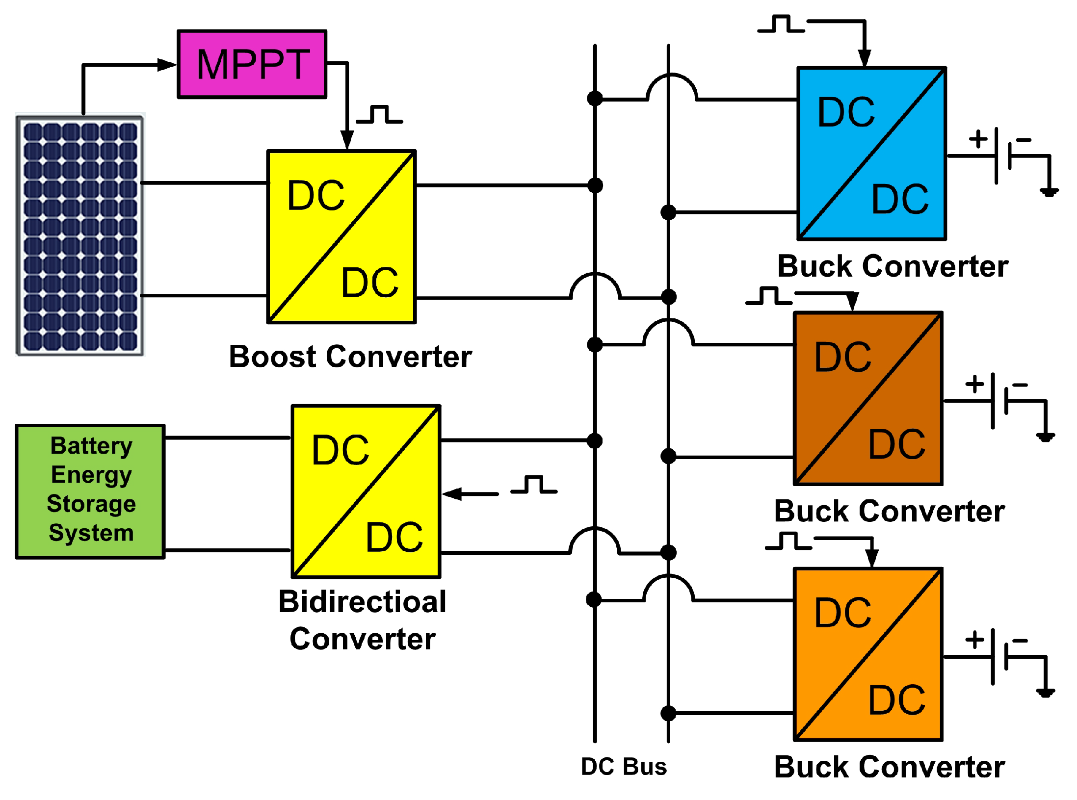
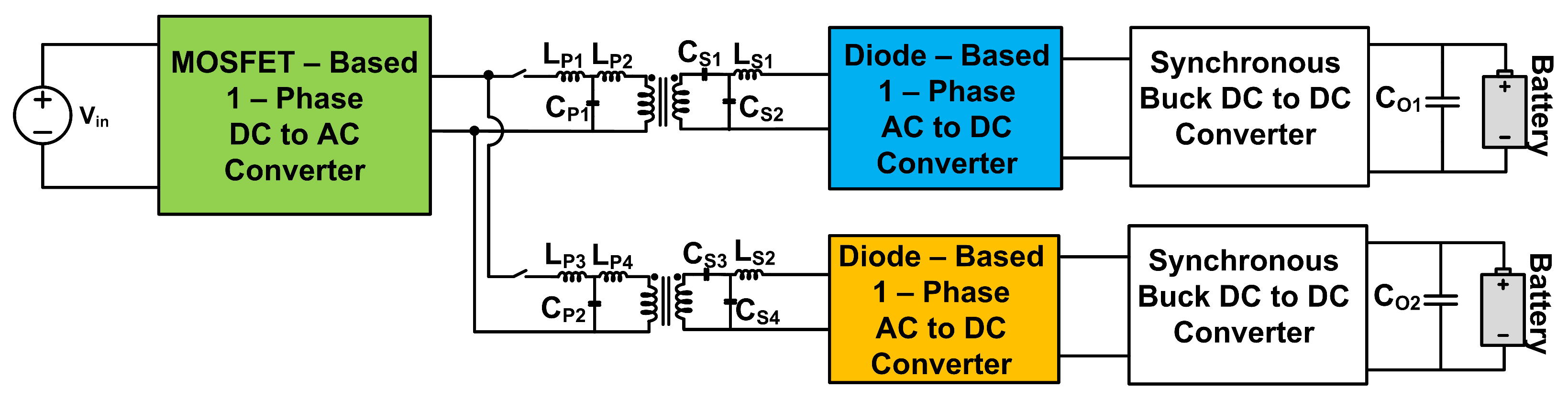
4. Simultaneous Charging Research: State of the Art

Only a few researchers have taken up experimental validation of simultaneous charging of EV batteries. Although it leads to the many advantages described in Section 2.3, the research focus has been relatively less compared to the focus on fast charging for charging time reduction. This section describes the various converters proposed by researchers working on simultaneously charging multiple batteries.
Mahafzah et al. [83] have proposed a synchronized multi-output hybrid buck-boost converter based on the Ćuk-Flyback topologies for renewable energy systems and electric vehicle applications. The proposed converter is shown in Figure 3. The design and steady-state analysis are provided for the proposed converter. The authors have presented the simulation results for a 300 W design to obtain a full-load efficiency of 90% at higher duty cycles close to 80 % . This is significantly higher than the conventional Flyback and Ćuk converters. For EV battery charging applications, the authors have proposed an AC-DC full-bridge PFC rectifier connected to the input terminals of the proposed converter. A simulation of a 1.5 kW system is provided to validate the idea. With the proposed AC-fed system, a power factor of 0.96 is obtained at the AC input side for an input of 200 V and 0.9401 for an AC input of 110 V. At these two input voltage levels, the THD is 27.69% and 36.25%, respectively. The work provides a novel multi-output converter fed from a single source. However, the converter is mainly suited for low-power EV charging at lower output voltage levels (such as a 48 V Li-ion battery).
Chen et al. [84] have considered the case of simultaneous charging as a constrained optimization problem to minimize simultaneous charging time. The block diagram of the solution proposed by the authors is shown in Figure 4. The authors have considered four objectives: convergence of State-Of-Charge (SOC) deviation, minimization of loss due to internal resistance, equating the SOCs of different batteries, and minimization of simultaneous charging time. The constraints are the SOC limitation of the batteries, the limitation on charging current, and the terminal voltage of the batteries. The authors have provided the battery pack model and developed the optimal charging strategy where trade-offs are made between the objective functions since it is impossible to optimize all objectives simultaneously to obtain a single solution to such problems. To tackle this problem, the authors have used the Adaptive Momentum-Based Steepest Descent (AMSD) algorithm and performed a simulation on the PLECS software platform with four battery packs and four Constant Voltage Current Sources (CVCS). For simulation, 3.1 Ah batteries have been considered, and the rating of the CVCS is 5 V. The simulation results have shown that the equilibrium time is reduced by more than 50 % compared to the quasi-sliding mode control. In addition, the convergence of the charging error is shown to be faster with the proposed algorithm. Experimental validation of the proposed method is provided by charging NCR 18650 3.1 Ah lithium-ion batteries (considered equivalent to battery packs). The experimental results have been used to show the superiority of the proposed algorithm over the battery-assisted charging system. The simultaneous charging time was observed to be minimum with the proposed algorithm, and the proposed system is said to prevent the over-charge and over-discharge of the battery. The work deals with simultaneous charging as an optimization problem focusing on reducing simultaneous charging time. However, the proposed system will have an increased component count for high-power EV battery charging applications, which may lead to lower reliability. If a diode rectifier is used for AC to DC conversion, there will be no control over the DC link side voltage when the input voltage changes. If a fully controlled rectifier is employed, the control becomes complex. With a full-bridge or its derived DC-DC converters, higher output voltage and power can be obtained, and it will be suitable for higher voltage battery charging, which will also involve reduced current, thereby reducing the losses in the secondary. Since the DC-DC converters can be designed based on the requirement of the charging station, the architecture proposed by the authors is very well suited for the simultaneous charging of vehicles with batteries of different voltage and power levels.
Aziz and Oda [13,85] have evaluated a battery-assisted quick-charging strategy for the simultaneous charging of EVs to reduce the burden on the grid. The proposed system is represented in Figure 5. The control server is considered to control the energy flow into all the parts of the community considering the related economics. The authors have considered the CHAdeMO standard for testing the charging of the quick chargers and the Li-ion battery for different seasonal conditions. A 50 kW inverter with an input voltage of 450 V and output RMS voltage of 200 V is considered, with the DC-DC converter feeding a 400 V battery with a maximum current of 150 A. The 64.2 kWh battery with a nominal voltage of 364.8 V and a maximum charging voltage of 393.6 V is considered. The 50 kW chargers are taken to have a variable DC output voltage of 50 to 500 V and a maximum output current of 125 A. The authors have concluded that the proposed battery-assisted system facilitates an increased charging rate and shorter charging time compared with the conventional system without battery support. This work describes the system for battery charging, and can be used for charging batteries at higher power and voltage. Better control is possible for the AC-DC and DC-DC converters to regulate the DC bus voltage and the charger output voltage. With full-bridge or dual active bridge (DAB) converter variants, higher power and voltage charging can be achieved at high efficiency. However, lower reliability could affect the system, and the control will be relatively complex.
Okon et al. [86] have described a CLLC-based charging circuit, shown in Figure 6, to charge a Li-ion battery using the CC-CV charging method. The operation is done in two stages, with the first stage providing control signals in progression and the second stage controlling the battery’s CC-CV charging. The authors have suggested creating a DC bus to connect multiple converters in parallel to enable multiple-battery charging. The authors have proposed a modified combined control system to control the proposed converter. The authors have provided simulation results obtained from PLECS software to validate the single battery charging. The authors have claimed that the system can be used for multiple-battery charging using the DC bus described above. Practical implementation has not been provided in this work for simultaneous battery charging. The proposed system is very well suited for high-power, high-efficiency battery charging, even with batteries with voltages greater than 400 V. On the other hand, the implementation of simultaneous battery charging will need a higher component count, thereby leading to an increase in the size and weight of the system.
Li et al. [87] have used two dual active bridge (DAB) converters with a rectifier and DC voltage divider to charge three Li-ion batteries, as shown in Figure 7. The proposed converter is a two-stage circuit. It uses a single-phase AC-DC converter, a DC voltage divider (using split capacitors with a neutral inductor and half-bridge configuration), and two parallel DAB converters. Two batteries are connected across the two split capacitors, and the DAB converter feeds the third battery. Correspondingly, control strategies are provided for the rectifier, the neutral leg circuit, and the two DAB converters. The rectifier is controlled using a double loop controller with a PI controller and a PR controller to obtain a constant DC voltage at the common node of the capacitors C1 and C2. The neutral leg is controlled using another double-loop controller with two PI controllers. The DAB converters are controlled using the concept of phase shift and feedback compensation. The circuit is fed from a 400 V, 50 Hz grid to obtain a DC link voltage of 560 V. A resistive load of 60 Ω is used instead of a battery for testing. Simulation and test results have been provided to validate the proposed system, considering a switching frequency of 4 kHz. The topologies proposed in work are well suited for high-power, high-voltage battery charging. The trade-off is with the higher number of components. The control is very flexible, specifically with DC-link voltage control. The two batteries that feed at the output terminals of the DC voltage divider have a common node. It would be preferable to isolate these two batteries to prevent current flow from one battery to the other.
Ramanathan et al. [88] have proposed a PV- and grid-fed modified impedance source inverter (ZSI) with transformers and full bridge rectifiers to charge two batteries simultaneously. The block diagram of the proposed circuit is shown in Figure 8. The maximum shoot-through duty ratio of the ZSI is calculated. Then the inductor and capacitor values are obtained. The system is configured to operate in four modes. Power flows from the PV to the grid in the first mode. The PV system charges the battery via the HFT in the second mode. In the third mode, the battery transfers energy to the grid through the inverter; in the fourth mode, the grid is used to charge the battery. The authors have considered the switching frequency of 20 kHz for the ZSI and 40 kHz for the half-bridge converter. A battery power of 200 W is considered. The authors have provided the simulation results from MATLAB/Simulink to show the simultaneous charging of the two equal-rated batteries. The system can be used up to a medium power level since it is fed from a single-phase supply. With the use of controlled rectifiers as proposed by the authors, it is possible to control the battery charging current for each battery. The system is not well suited for higher voltage batteries.
Graw and Zimmermann [89] have proposed a boost-flyback converter combination to charge battery stacks separately from a renewable energy source. The work aims to simultaneously charge both a high voltage (HV) battery and a low voltage battery from a single source. The authors have explained the modes of operation of the proposed converter with the corresponding timing diagrams and the design of the flyback transformer. Overcharging the LV battery is prevented by redirecting the power to the HV battery, leading to simpler control. The effect of the capacitance between the adjacent transformer windings has been evaluated, and the effect on efficiency is noted. The authors have also considered the effect of adding an LC snubber as a method to reduce the MOSFET drain peak voltage. The proposed system is a combination of an isolated and a non-isolated converter. It can be used only for power levels below 100 W and is unsuitable for fast charging. The system has common ground between the secondary and primary due to the combination of the non-isolated and isolated converters. The circulating current from the HV battery to the LV battery is possible due to this. It could also lead to EMI issues when etched on a PCB.
Sun et al. [90] have proposed an isolated multi-port DC charging station as a part of a smart grid system. The block diagram proposed by the authors is shown in Figure 9. The HV stage employs a cascaded H-bridge converter, and the isolation stage uses multiple cascaded DAB converters. The DC side of all the DABs is connected to the DC bus, which charges multiple batteries simultaneously using separate chargers. Dual-loop control is used for the rectifier stage, while the voltage control strategy with a current balancing function controls the DAB stage. Both Grid-to-Vehicle (G2V) and Vehicle-to-Grid (V2G) are employed in the charging module. The authors have provided the simulation results for the proposed system. The simulation system comprises 24 rectifier modules, each connected in series with a DAB operating at a switching frequency of 10 kHz. The three batteries are at voltage levels of 300 V with capacities of 15 kWh, 15 kWh, and 20 kWh, with different SOCs. The objective of the work is to validate the proposed topology, which has been done using simulation. The hardware implementation of the proposed system has not been provided in the work. The system is very well suited for high voltage batteries as described by the authors. However, the intermediate conversion stage has a very high number of devices, which may lead to poor reliability in real-time implementation.
In Ref. [91], the authors Yesheswini et al. have proposed a DC-DC converter-based system for charging multiple EVs simultaneously. The system is a solar-fed battery charging system with a boost converter, backup battery, bidirectional converter, and buck converter to charge EV batteries. The system proposed by the authors is shown in Figure 10. The authors have chosen a 36 V, 28 Ah lead-acid battery for simulation. The solar PV source is chosen to be composed of two 180 W panels connected in parallel. The solar-fed converter is controlled using the perturb and observe (P&O) maximum power point tracking (MPPT) algorithm, while the battery charging is simulated using the CC-CV charging algorithm. A bidirectional converter connects the station battery with the DC grid, facilitating charging and discharging based on the requirement. The station battery will support the charging whenever the solar PV supplies low power (lower than the EV requirement). The station battery will be charged when the solar power is in excess. The station battery is also used to maintain a constant DC bus voltage. The hardware prototype is implemented using a lead-acid battery with the buck converter (with IRFP460 MOSFET) controlled using an STM controller. The switching frequency is chosen to be 4 kHz. The authors have analyzed the performance of the converters for EV battery charging. As a future scope, the authors have suggested optimizing sources such as solar, wind, and biofuels, using various controllers and machine learning methods to optimize the load on the charging station. The proposed system has used solar and battery energy storage systems as the two sources. Therefore, the current rating will be limited, especially considering the intermittency of solar energy. Since the system does not involve a grid connection, so that power will be limited, it is hence not very suitable for fast charging.
Mishra et al. [92] have proposed a grid and solar-based hybrid charger that is controlled using adaptive supervisory control (ASC). The topology used by the authors is shown in Figure 11. The proposed topology uses two isolated converter stages (one DAB and one resonant converter), one working as a slow charger and the other as a fast charger. In addition, a PV-fed DC-DC converter with a battery storage unit (BSU) is considered as shown in the figure. The grid-side converter (GSC) is an active bridge AC to DC converter used to regulate the DC link voltage and to ensure PFC. It is operated at a frequency of 10 kHz. A PR controller-based closed loop is used to control the GSC. In the PV-fed converter, the incremental conductance algorithm is implemented for MPPT. The BSU is the battery pack with a buck-boost bidirectional converter. The DAB is controlled to have zero voltage switching (ZVS) with bidirectional power transfer. When only the grid supplies power, the slow charger is utilized to charge the EV batteries, while slow and fast chargers are used when both the grid and PV supply power to ensure minimal stress on the grid. The proposed system is very suitable for simultaneous fast and slow charging. Battery swapping function is added along with a storage unit that can be used as a backup source. The proposed system can be used to charge high-power, high-voltage batteries. However, a higher number of components could pose reliability issues.
In Ref. [93], Vu et al. have proposed using a multi-input capacitive coupled wireless charger for EV battery charging. The block diagram is shown in Figure 12. Capacitive power transfer (CPT) topologies have high leakage capacitance, which is usually compensated for by using resonant inductors. However, the authors have pointed out that this method is unsuitable for high-power applications, and that LCL topology is more suitable. The authors have provided a detailed analysis of the CPT system. A DC input voltage of 250 V is chosen with a variable output of 120 to 270 V. The switching frequency of 1 MHz is chosen for the system. Cross-coupling is avoided by selecting a distance of 150 cm between both primary plates. Simulation results are provided for the proposed system for equal and unequal load conditions of the two converters. With the wireless power transfer of the capacitive type, the main issue is the distance of separation between the transmitter and the receiver. In addition, the efficiency of wireless transfer is less. With the use of diode rectifiers as proposed by the authors, the receiver side circuit also needs to be controlled from the transmitter side, making the control less flexible.
Fan et al. [94] have proposed a reflex charging technique to charge two batteries simultaneously. The authors have used ‘N’ sets of interleaved buck-boost converters to obtain reflex charging. The modes of operation and the corresponding equivalent circuits have been explained. Phase shift control has been employed to control the converters in this work. This is also said to prevent over-charging or over-discharging. In addition, a battery charge-discharge management system has been proposed to maintain the battery voltage. The authors have validated the system by charging two 12 V batteries from 17 to 24 V input. The experiment for N = 1, 2, 3, and 4 sets have been provided. Both positive and negative battery currents have been obtained, validating the two states of operation based on the power switch operation. Since the proposed system uses buck-boost converters, isolation is not provided and is only suitable for low-power charging at lower voltages.
Vu et al. [95] have proposed a multi-output inductive wireless power transfer (WPT) charger for simultaneously charging two batteries. A standard full-bridge voltage source inverter is used to convert DC input to AC, which is then passed to two compensation networks of inductors and capacitors with high-frequency transformers, which feed two diode rectifiers separately in cascade with synchronous buck converters (SBCs). The output of the SBCs is used to supply the two batteries, which charge simultaneously. The circuit diagram proposed by the authors is shown in Figure 13. The AC equivalent circuit of the inductive power transfer system with its analysis has been provided to calculate the coupling coefficient. The frequency is kept constant during the operation, and the secondary side converter functions as the charger controller. The resonant tank circuit components design has been provided for the proposed converter. A DC input voltage of 400 V is chosen to obtain a variable output of 250 to 400 V. A switching frequency of 68 kHz was used for the simulation. Unequal loads have been used to simulate the system to validate the circuit operation and simultaneous charging of both batteries. With WPT, the two primary challenges are the separation distance between the two coils and the lower efficiency of power transfer. The proposed system can be used to charge batteries of unequal ratings. Synchronous buck converter provides better control possibility but limits the power. Hence the system is not very suitable for fast charging.
Chakraborty et al. [96] have proposed a pulse charging-based Li-ion battery charging converter. The main power supply working as a current source (equivalent) is connected in a predefined order, in parallel, with different batteries using a set of switches. At any given time, one battery is being charged. This is decided by turning the selector switch (S1, S2 or S3) ON and OFF to connect or disconnect the respective battery. If all batteries are charged, a reset switch is used for freewheeling the inductor energy. The controlled current source uses the forward converter topology with a core reset. A number of MOSFETs and diodes are used to implement the switch selectors. For ‘n’ battery cells connected in series in each switch selector block, 2n+2 MOSFETs and 2n diodes are required. Thus, if three battery cells are connected in series for one switch block, say, S1, then eight MOSFETs and six diodes are required for making that selector switch. Charge balancing is implemented along with charging and discharging using the pulse charging technique. A two-output case is simulated using the parameters of the VALENCE 444 Li-polymer cell. The converter is fed from a 170 V AC supply with the maximum duty cycle limited to 44 % . The switching frequency selection is flexible, and average current control is used to control the inductor current. The proposed system uses a higher number of components, especially when multiple batteries are to be charged simultaneously. In addition, the power limitation leads to slow charging and is not suited for charging vehicles at higher voltages.
In continuation with the previous work [96], Chakraborty and Mohan [97] have extended the work to a wider range of medium-power AC-DC applications. The suitability of CCM and DCM has been evaluated. Negative voltage feedback reduces the bus voltage stress, with a trade-off that includes an increase in the input current distortion. The advantages of the voltage doubler rectifier topology are provided in detail, and the corresponding simulation waveforms have been provided. The input current THD is around 60% and a simulation efficiency of 84 % has been obtained with an input of 110 V AC.
Table 1 gives a comparison of the various converters described in Section 4.

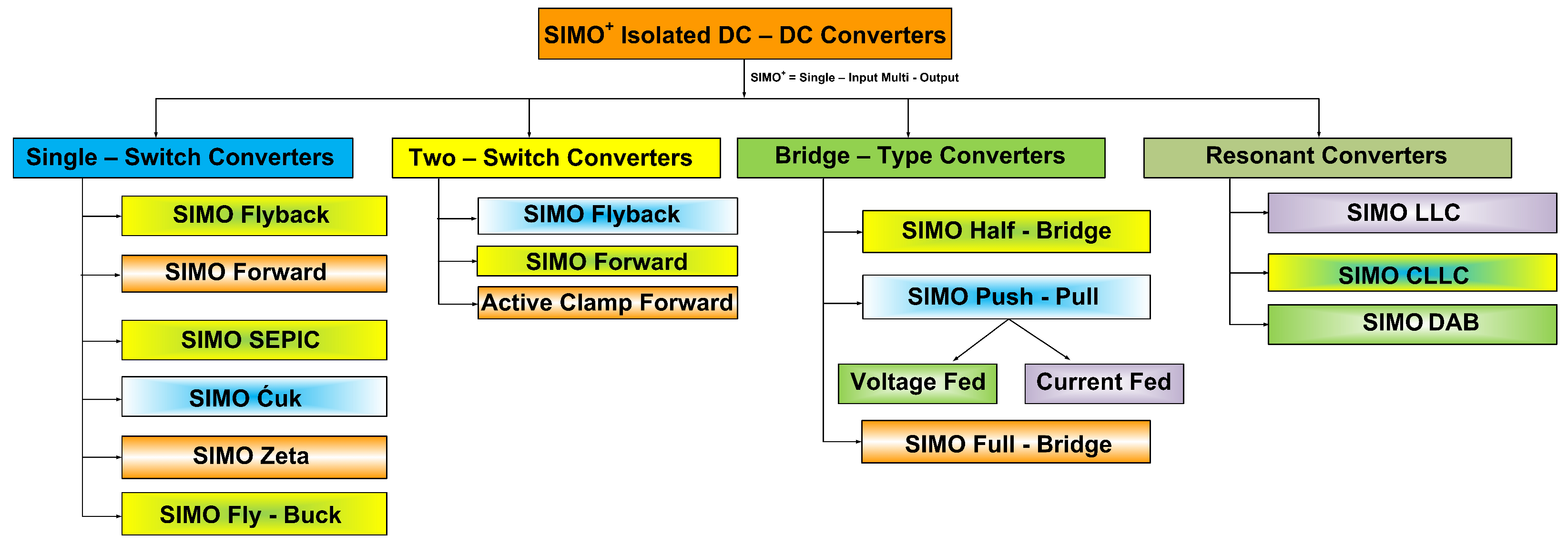
5. Potential Extension of Existing Isolated DC-DC Converters for Simultaneous Charging of Multiple EV Batteries

Simultaneous charging of multiple EV batteries requires multi-output DC-DC converters. For high-power applications such as battery charging, isolated converters are preferred. While several isolated DC-DC converter topologies exist in the literature, all the topologies cannot be used to get the same performance characteristics for EV battery charging applications. This section provides some potential isolated DC-DC converter configurations for simultaneously charging multiple Li-ion batteries. Galvanic isolation is required between the different circuits of the charger to ensure safe and reliable operation [42]. A classification of the most common Single-Input Multi-Output (SIMO) Isolated DC-DC converters is shown in Figure 14.
The choice of a DC-DC converter for EV battery charging depends on the following factors [98]:
  • Power rating and power density;
  • Isolation requirement;
  • Charging type (AC/DC charging, slow/fast charging);
  • Current rating (affects the choice of cable);
  • Type of switch used (depends on the frequency of switching, which decides the magnetic component size);
  • Number of outputs required;
  • Voltage at each of the output terminals;
  • Cost, size, and weight of the system.
The appropriate topology is to be chosen based on the trade-offs between the factors. With the mass usage of EVs, infrastructure needs to be developed to facilitate charging. The infrastructure in developed countries is better than that in developing nations. During infrastructure development, the land size, availability of power supply, the possibility of extension for future needs, types of vehicle, charging station layout, cabling cost, distance, incentives, and other factors need to be considered [99]. Location, cost, waiting time, charging time, and payment options are some of the most critical factors from the consumer’s point of view [100]. The locations could include workplace parking areas, shopping malls, and public parking structures [99]. The waiting time needs to be reduced in addition to the reduction of charging time to attract consumers to a particular charging station. Presently available infrastructure will significantly affect the further expansion and installation of new chargers. In this scenario, many of the above-mentioned factors will be predefined and can pose some limitations during expansion. Care has to be taken, especially regarding the ratings of the components, protection system, and communication protocols during expansion. The expansion needs to be planned, modeled, and programmed considering the present infrastructure along with the pattern of transportation expansion [101]. It can be taken up as an optimization problem with the existing infrastructure limits as the constraints [102].
Section 5.1, Section 5.2, Section 5.3, Section 5.4 and Section 5.5 describe the various converters that can simultaneously charge two or more batteries. Some converters are limited to low-power applications, while others can be used for high-power applications. All descriptions related to this are provided in this section. In addition, power loss estimation (assuming ideal passive elements) is described for the converters that are more commonly used for battery charging.

5.1. Single-Switch Isolated DC-DC Converters

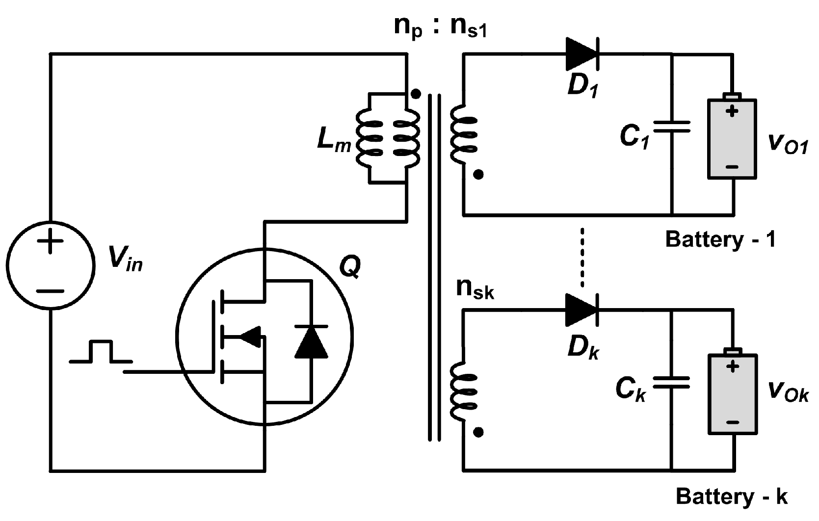
5.1.1. Single-Switch Multi-Output Flyback Converter

The flyback converter is an isolated buck-boost topology that can be modified to implement multi-battery charging. The basic flyback converter uses one active switch (MOSFET/IGBT), diode, capacitor, and transformer. Theoretically, ‘k’ number of batteries can be charged using a flyback converter if a transformer with ‘k’ number of isolated secondaries is used [103], as shown in Figure 15. Getting multiple outputs does not involve much difference in complexity, space, or cost since each additional output requires one HFT, one diode, and one capacitor. The converter gives relatively good efficiency at a low cost. The equation for each of the outputs (in CCM) is given by Equation (2), where δ is the duty cycle. However, this topology has one major limitation. The typical power limitation of a flyback converter is approximately 60 W [104] (less than 100 W, in general). Hence, the converter could charge and discharge the low-voltage auxiliary battery of the EV or low-power vehicles such as e-bicycles or low-power two-wheelers. The other disadvantages include high stress on the switch, relatively higher conduction losses, and the requirement of a snubber. The choice of switching frequency and ratings of the various components depends on the type of source available and the rating of the battery, which will decide the duty cycle value. The design of the multi-secondary flyback transformer is a critical design criterion that needs to be considered. The magnetizing inductance value needs to be greater than a minimum value ( L m , m i n ) to ensure CCM. This is given by Equation (3). To ensure CCM operation, the inductance value should be greater than L m , m i n value. Since the inductance chosen should be greater than L m , m i n , it could lead to design issues if too high or too low inductance is chosen. Hence, the required inductance can be calculated using Equation (4) and then verified if it is greater than L m , m i n or not.
v O k = n s k n p · δ 1 δ · V i n
L m , m i n = k × ( 1 δ ) 2 2 × f s w · n s k 2 n p 2
L m = k × V i n × δ Δ i L m × f s w
The capacitance of the capacitor across the load can be calculated using Equation (5), where R is the equivalent load resistance.
C k = v O × δ Δ v O × R × f s w
A capacitor (Cin) can be connected across the source if the input is noisy. Such a capacitance can be calculated using Equation (6).
C i n = i i n × t o f f 2 × Δ v c i n
The semiconductor utilization factor ( S U F ) is given by Equation (7). A plot of S U F for duty cycles from 0 to 1 is shown in Figure 16. It can be seen from the graph that the S U F is the highest when the converter is operated at a duty cycle of 50% [105]. Therefore, it is better to operate the flyback converter at or around the duty cycle values of 50%.
S U F = δ δ 2 δ + 1 δ
The conduction losses in the MOSFET and each diode can be estimated using Equations (8) and (9), respectively [105].
P c o n d , Q = V t h · I i n + r D S , O N · i i n 2 δ + δ · Δ i L m 2 3
P c o n d , D K = V t h · I O + r O N D k ( 1 δ ) i i n n p δ n s k 2 + Δ i L m · n p n s k 2 3
where r D S , O N is the on-state resistance of the MOSFET, r O N D k is the on-state resistance of the diode, I i n is the average value of the input current, and V t h is the threshold voltage of the corresponding device (MOSFET or diode). Based on the turn-off energy loss characteristic ( w o f f , D K , x o f f , D K and y o f f , D K ) provided by the manufacturer for the 100FIT test voltage ( V 100 F I T ; it is the voltage across the device such that there are 100 failures within 10 9 h of operation [106]; FIT is Failures In Time), we can estimate the average value of the switching loss in the diode [105] using Equation (10).
P s w , D K = V O δ + Δ v o T s w V 100 F I T · w o f f , D K · I i n δ Δ i L m n p n s k 2 + x o f f , D K · I i n δ Δ i L m n p n s k + y o f f , D K
Similarly, the average value of the switching loss [105] in the MOSFET ( P s w , Q ) is estimated using Equation (11).
P s w , Q = V i n ( 1 δ ) Δ v o n p n s k T s w V 100 F I T · w o f f , S W · I i n δ + Δ i L m 2 + x o f f , S W · I i n δ + Δ i L m + y o f f , S W + V i n ( 1 δ ) + Δ v o n p n s k T s w V 100 F I T · w o n , S W · I i n δ Δ i L m 2 + x o n , S W · I i n δ Δ i L m + y o n , S W
where w o f f , S W , x o f f , S W and y o f f , S W are the turn-off energy loss characteristic provided by the manufacturer for V 100 F I T , and w o n , S W , x o n , S W and y o n , S W are the turn-on energy loss characteristic from the MOSFET data-sheet.

5.1.2. Single-Switch Multi-Output Forward Converter

The other popular isolated converter is the forward converter. It is an isolated version of the popular buck converter. Compared to a flyback converter, it gives a faster transient response, better efficiency, and low output ripple. However, the cost is higher when compared to that of a flyback converter. It is generally used whenever a high current output is required [107]. The major limitation of the forward converter is the duty cycle. Its maximum duty cycle must be about 50%. The forward converter uses a tertiary winding ( n t e r ) and a diode to enable core reset. The high-voltage winding usually provides the core reset. The time taken to reset is inversely proportional to the winding voltage. Figure 17 shows the implementation of a forward converter with multiple winding to enable simultaneous charging of batteries. Similar to a flyback converter, the forward converter also has a power limitation of 100 W [103]. The output of the kth winding is related to the input as given by Equation (12). The magnetizing inductance ( L m ), output inductance ( L k ) and output capacitance ( C k ) can be found using Equations (13), (14) and (15), respectively. If the input is noisy, a capacitor ( C i n ) with a value calculated using Equation (16) can be connected across the source.
v O k = n s k n p · δ · V i n
L m = k × V i n × δ f s w × Δ i L m
L k = V O × ( 1 δ ) f s w × Δ i L k
C k = V O × ( 1 δ ) 8 × Δ V O × L k × f s w 2
C i n = ( I i n + Δ i L m ) · T o f f 2 · Δ v C i n
The semiconductor utilization factor ( S U F ) for the forward converter [105] is given by Equation (17). The choice of transformer turns ratio ( n s k : n p ) plays a vital role in obtaining optimal semiconductor utilization factor since the S U F depends on δ m a x , which depends on the transformer turns ratio. Optimal S U F leads to optimal converter design. A plot of duty cycle ( δ ) vs. S U F can be plotted to obtain the corresponding optimal turns ratio of the transformer. An example of such a plot is shown in Figure 18 for various δ m a x between 0.2 and 0.9 .
S U F = ( 1 δ m a x ) · δ ( 1 + δ m a x ) · δ + ( 1 δ m a x ) · 1 δ
The average value of conduction loss of the switch Q, and three diodes D 0 , D 1 k , and D 2 k are given by Equations (18), (19), (20), and (21), respectively [105].
P c o n d , Q = V t h · ( I i n + Δ i L m · δ ) + r D S , O N · δ · I O · n s k n p + Δ i L M 2 + Δ i L m + Δ i L 1 n s k n p 2 3
P c o n d , D 0 = V t h · Δ i L m · δ + r D S , O N · ( 2 · Δ i L m ) 2 · n p n t e r · δ 3
P c o n d , D 1 k = V t h · I O · δ + r D S , O N · δ Δ I O 2 + Δ i L k 2 3
P c o n d , D 2 k = V t h · I O · ( 1 δ ) + r D S , O N · ( 1 δ ) Δ I O 2 + Δ i L k 2 3
Before calculating the switching losses, we note that the switching loss in diode D 0 is negligible since it is turned OFF when the current reaches zero. Therefore, switching losses must be calculated for switch Q and diodes D 1 k and D 2 k . The corresponding switching losses are estimated using Equations (22), (23) and (24), respectively [105]. The W, x and y coefficients have the same meaning as described before.
P s w , Q = 1 + n p n t e r · ( V i n Δ v C i n ) T s w V 100 F I T · w o f f , S W I O + Δ i L k n s k n p + 2 · Δ i L m 2 + x o f f , S W I O + Δ i L k n s k n p + 2 · Δ i L m + y o f f , S W + 1 + n t e r n p · ( V i n + Δ v C i n ) T s w V 100 F I T · w o n , S W I O Δ i L k n s k n p 2 + x o n , S W I O Δ i L k n s k n p + y o n , S W
P s w , D 1 k = n s k n t e r · ( V i n Δ v C i n ) T s w V 100 F I T · w o f f , D 1 k I O + Δ i L k 2 + x o f f , D 1 k I O + Δ i L k + y o f f , D 1 k
P s w , D 2 k = n s k n t e r · ( V i n + Δ v C i n ) T s w V 100 F I T · w o f f , D 2 k I O Δ i L k 2 + x o f f , D 2 k I O Δ i L k + y o f f , D 2 k

5.1.3. Single-Switch Multi-Output Isolated SEPIC

The Single-Ended Primary Inductor Converter (SEPIC) is a popular buck-boost-derived converter. A transformer replaces the inductor of the non-isolated SEPIC with proper dot polarity to obtain the isolated version of the converter. This converter can be modified to charge multiple batteries simultaneously, as shown in Figure 19. It provides an output voltage described by Equation (25). The advantage of isolated SEPIC is that the input current has low ripple and hence is suited very well when the input to the charger is provided from solar PV panels. Adding multiple outputs does not significantly increase cost since each additional stage requires only an HFT, a diode, and a capacitor. The input inductance, input capacitance, magnetizing inductance, and output capacitance are calculated using Equations (26), (27), (28), and (29), respectively [105].
v O k = n s k n p · δ 1 δ · V i n
L 1 = k × V i n 2 × Δ i L 1 × f s w · δ
C 1 = k × I O 2 × Δ v C 1 × f s w · n s k n p · δ
L m = k × V i n 2 × Δ i L m × f s w · δ
C k + 1 = I O 2 × Δ v C 1 × f s w · n s k n p · δ
The semiconductor utilization factor of an isolated SEPIC is the same as that of a flyback converter and is given by Equation (7). The conduction losses in the MOSFET (Q) and diode ( D k ) can be estimated using Equations (30) and (31), respectively [105].
P c o n d , Q = V t h I i n + r D S O N I i n 2 δ + δ Δ i L 1 + Δ i L m 2 3
P c o n d , D K = V t h , D K I O + r O N D k ( 1 δ ) I i n δ n p n s k 2 + n p n s k 2 Δ i L 1 + Δ i L m 2 2 3
where r O N D k is the ON-state resistance of the diode and V t h , D K is its threshold voltage. The average switching loss P s w , D k in diode D K [105] is given by Equation (32).
P s w , D k = V i n ( 1 δ ) + Δ v C 1 · n s k n p + Δ v C k T s w · V 100 F I T · W + X + Y
where,
  • W = w o f f , D k · I i n Δ i L 1 Δ i L m · n p n s k + I O 2
  • X = x o f f , D 1 · I i n Δ i L 1 Δ i L m · n p n s k + I O
  • Y = z o f f , D 1
The average switching loss of the switch Q can similarly be found [105] using Equation (33).
P s w , S W = V i n ( 1 δ ) Δ v C 1 Δ v C ( k + 1 ) n p n s k T s w · V 100 F I T U + V + W + V i n ( 1 δ ) + Δ v C 1 + Δ v C ( k + 1 ) n p n s k T s w · V 100 F I T X + Y + Z
where,
  • U = w o f f , S W · I i n + Δ i L 1 + Δ i L m + I O · n s k n p 2
  • V = x o f f , S W · I i n + Δ i L 1 + Δ i L m + I O · n s k n p
  • W = y o f f , S W
  • X = w o n , S W · I i n Δ i L 1 Δ i L m + I O · n s k n p 2
  • Y = x o n , S W · I i n Δ i L 1 Δ i L m + I O · n s k n p 2
  • Z = y o n , S w

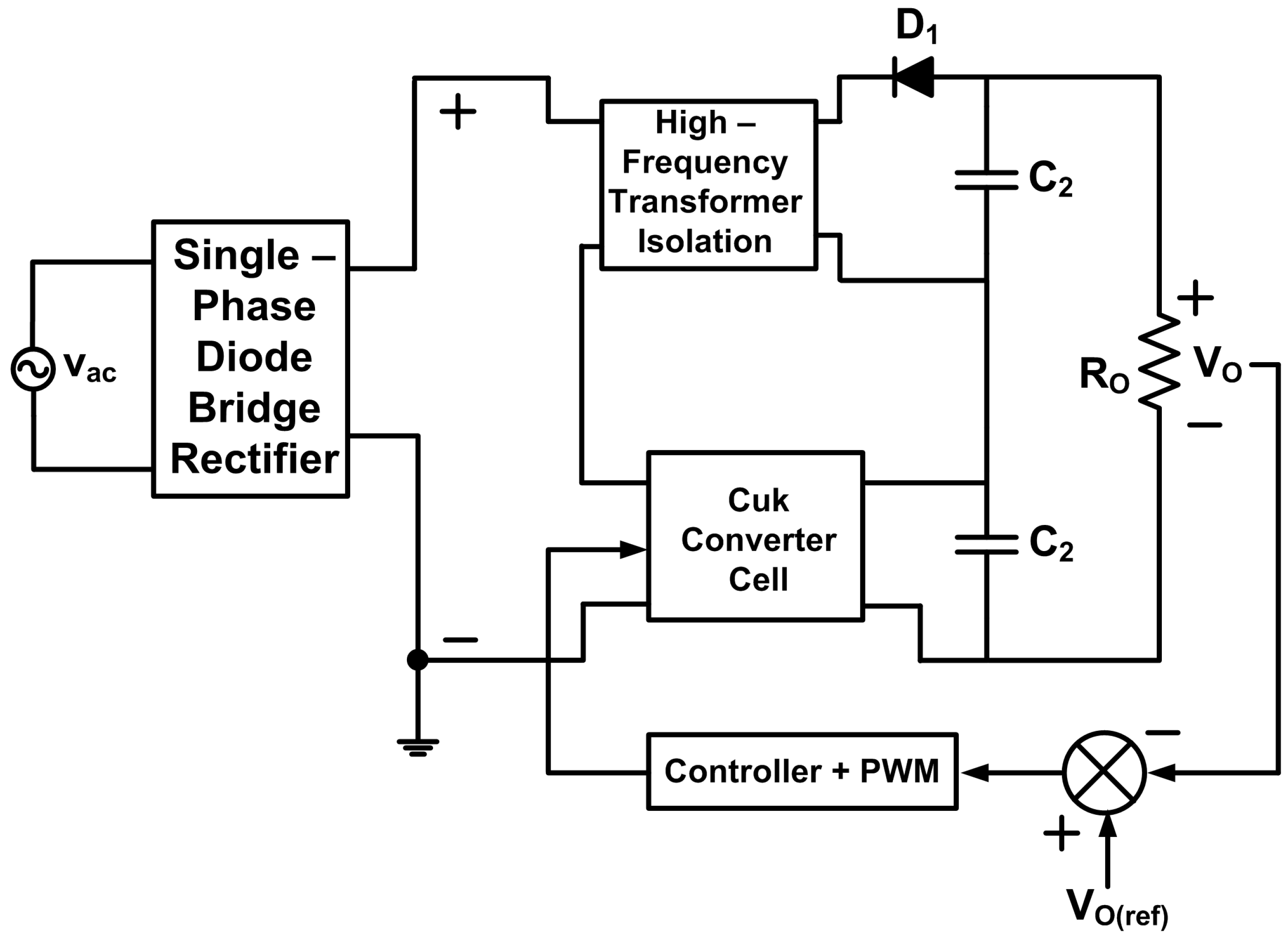
5.1.4. Single-Switch Multi-Output Isolated Ćuk Converter

The Ćuk converter is another popular buck-boost-derived converter. It was invented and patented by Slobodan M. Ćuk and Robert D. Middlebrook [108]. The non-isolated Ćuk converter can be modified to obtain the isolated version of the converter. This can further be modified to charge multiple batteries simultaneously, as shown in Figure 20. It provides an output voltage that is described by Equation (25), and the design [105] of the inductance and capacitance of the inductors and capacitors are calculated using Equations (34) through (39).
L 1 = k × V i n 2 × Δ i L 1 × f s w · δ
L m = k × V i n 2 × Δ i L m × f s w · δ
L k + 1 = V i n 2 × Δ i L ( k + 1 ) × f s w · δ
C 1 a = k × I O 2 × Δ v C 1 × f s w · n s k n p · δ
C k b = I O 2 × Δ v C 1 × f s w · δ
C k + 1 = Δ i L 2 8 × Δ v C ( k + 1 ) × f s w
Considering the average value input current represented by Iin, the average conduction loss in the MOSFET Q [105] is given estimated using Equation (40).
P c o n d , S W = V t h I i n + r D S , O N I i n 2 δ + δ Δ i L 1 + Δ i L m + Δ i L ( k + 1 ) · n s k n p 2 3
The average conduction loss in the diode D k [105] is given by Equation (41).
P c o n d , D k = V t h , D K I O + r O N D k ( 1 δ ) I i n δ n p n s k 2 + Δ i L 1 + Δ i L m ) n p n s k + Δ i L ( k + 1 ) 2 3
The average switching loss in diode D k [105] is estimated using Equation (42).
P s w , D k = V i n ( 1 δ ) + Δ v C 1 a n s k n p + Δ v C k b T s w V 100 F I T W + X + Y
where,
  • W = w o f f , D k I i n Δ i L 1 Δ i L m n p n s k + I O Δ i L ( K + 1 ) 2
  • X = x o f f , D k I i n Δ i L 1 Δ i L m n p n s k + I O Δ i L ( k + 1 )
  • Y = y o f f , D k
The average switching loss of of the switch Q [105] can similarly be estimated using Equation (43).
P s w , Q = V i n ( 1 δ ) Δ v C 1 a Δ v C k b · n p n s k T s w · V 100 F I T · U + V + W + V i n ( 1 δ ) + Δ v C 1 a + Δ v C k b · n p n s k T s w · V 100 F I T · X + Y + Z
where,
  • U = w o f f , S W · I i n + Δ i L 1 + Δ i L m + I O + Δ i L 2 n s k n p 2
  • V = x o f f , S W I i n + Δ i L 1 + Δ i L m + I O + Δ i L ( k + 1 ) n s k n p
  • W = y o f f , S W
  • X = w o n , S W I i n Δ i L 1 Δ i L m + I O Δ i L ( k + 1 ) n s k n p 2
  • Y = x o n , S W I i n Δ i L 1 Δ i L m + I O Δ i L ( k + 1 ) n s k n p 2
  • Z = y o n , S W

5.1.5. Single-Switch Multi-Output Isolated Zeta Converter

A Zeta converter is a modified buck-boost converter, and its isolated version uses one transformer, one inductor, one capacitor, one active switch, and one diode. An isolated Zeta converter is emerging as an attractive option for EV battery charging as it gives a very stable response and requires minimal control. The isolated zeta converter modified to charge multiple batteries is shown in Figure 21. The relationship between the output and input voltages is given by Equation (25). The inductance L m of the magnetizing inductance and the inductor L k is calculated using Equations (44) and (45), respectively. The capacitance of the capacitors C 1 k and C 2 k are given by Equations (46) and (47), respectively.
L m = k × V i n × δ f s w × L m
L k = n s k n p · V i n × δ f s w × L k
C 1 k = v O × δ f s w × R × Δ v C 1 k
C 2 k = v O × ( 1 δ ) 8 × f s w 2 × L k × Δ v C 2 k

5.1.6. Single-Switch Multi-Output Isolated Buck (Fly-Buck) Converter

The single-switch fly-buck converter is shown in Figure 22 for multiple-battery charging. The converter has a capacitor C 1 across which the first output can be taken (shown across C 1 as a small battery of voltage V a u x ) . This can be used to charge the low-voltage auxiliary battery. The secondary windings can charge other batteries based on the transformer turns ratio. The equations for output voltages are given by Equations (48) and (49).
v a u x = V i n × δ
v O k = n s k n p × v a u x

5.2. Two-Switch Isolated DC-DC Converters

5.2.1. Two-Switch Flyback Converter

The two-switch flyback converter is used to overcome the typical problems of a single-switch flyback converter. The topology can be used for multi-battery charging, as shown in Figure 23. It can also be modified into a quasi-resonant flyback converter (a DCM Flyback having a valley switching turn on). The output voltage equation is the same as the flyback converter (Equation (2)). The same pulse is provided to both the switches of the converter. The two-switch flyback converter has better efficiency since the clamping losses are removed by recycling the leakage energy to the input side through the two diodes. This also implies reduced thermal stress on the switch. The overall voltage stress is divided between the two MOSFETs [109]. In this topology, the maximum duty cycle limitation is 0.5 when operating in continuous conduction mode [109].

5.2.2. Two-Switch Forward Converter

The two-switch forward converter feeding multiple batteries is shown in Figure 24. The output voltage is given by Equation (50). It is usually used between 150 W and 750 W [110]. The circuit has multiple advantages, including no body-diode conduction, no snubber requirement, and the possibility of handling multiple isolated outputs. It does not require any dead-time and does not suffer from the problem of a potential shoot-through. However, the frequency of operation is limited due to its inability to switch at zero voltage [110] and requires a relatively larger transformer since it is a single-ended converter. The minimum value of inductance Lk is given by Equation (51), and the maximum value of the duty cycle is limited to 50% [111].
v O k = n s k n p × δ × V i n
L k , m i n = k × V O × ( 1 δ m i n ) 2 × f s w × I O , B
where IO,B is the output current at the CCM/DCM boundary, given by,
I O , B = V O R L o a d , m a x
The semiconductor utilization factor ( S U F ) for the two-switch forward converter is given by Equation (53). The plot of duty cycle vs. S U F for this converter is presented in Figure 25.
S U F = δ ( 3 · δ ) + 1 δ
The conduction loss in the diode D k is given by Equation (54) and that in switch Q is given by Equation (55).
P c o n d , D k = V t h · Δ i L m · δ + r D S , O N · ( 2 · Δ i L m ) 2 · δ 3
P c o n d , Q = V t h · ( I i n + Δ i L m · δ ) + r D S , O N · δ · I O · n s k n p + Δ i L M 2 + Δ i L m + Δ i L 1 n s k n p 2 3
The average value of conduction losses in diodes D p 1 and D p 2 are estimated using Equations (56) and (57), respectively.
P c o n d , D p 1 = V t h · I O · δ + r D S , O N · δ Δ I O 2 + Δ i L k 2 3
P c o n d , D p 2 = V t h · I O · ( 1 δ ) + r D S , O N · ( 1 δ ) Δ I O 2 + Δ i L k 2 3
Similarly, the average switching losses can be estimated for the MOSFET, and diodes D p 1 and D p 2 using Equations (58), (59), and (60), respectively.
P s w , Q = ( V i n Δ v C i n ) T s w V 100 F I T · w o f f , S W I O + Δ i L k n s k n p + 2 · Δ i L m 2 + x o f f , S W I O + Δ i L k n s k n p + 2 · Δ i L m + y o f f , S W + ( V i n + Δ v C i n ) 2 · T s w V 100 F I T · w o n , S W I O Δ i L k n s k n p 2 + x o n , S W I O Δ i L k n s k n p + y o n , S W
P s w , D p 1 = n s k n p · ( V i n Δ v C i n ) T s w V 100 F I T · w o f f , D p 1 I O + Δ i L k 2 + x o f f , D p 1 I O + Δ i L k + y o f f , D p 1
P s w , D p 2 = n s k n p · ( V i n + Δ v C i n ) T s w V 100 F I T · w o f f , D p 2 I O Δ i L k 2 + . x o f f , D p 2 I O Δ i L k + y o f f , D p 2

5.2.3. Push-Pull Converter

The push-pull topology is another isolated converter that can charge multiple batteries simultaneously. Figure 26 shows the push-pull converter topology used to charge two batteries. The output voltages of the push-pull converter feeding two batteries are given by Equations (61) and (62).
v O 1 = 2 × n s 1 n p 1 × δ × V i n
v O 2 = 2 × n s 2 n p 1 × δ × V i n
The semiconductor utilization factor ( S U F ) for a push-pull converter is given by Equation (63), and a plot of duty cycle vs. S U F is provided in Figure 27. From the equation of S U F , it can be inferred that the SUF would be imaginary for duty cycles greater than 50%. Hence, δ 50 % is the duty cycle limitation for a push-pull converter.
S U F = δ ( 2 · δ ) + 1 ( 2 · δ )
The average value of conduction losses in switches Q 1 and Q 2 are estimated using Equations (64) and (65), respectively. Similarly, the average conduction losses in the diodes on the secondary side are estimated using Equations (66) and (67), respectively. We must note that the conduction loss in diodes D 1 and D 2 are equal and that in D 3 and D 4 are equal. Hence, the loss equations for D 1 and D 3 have been presented.
P c o n d . Q 1 = v t h · I i n 2 + r D S , O N · δ · I O n s 1 n p 1 2 + Δ i L m + I L 1 n s 1 n p 1 2 3
P c o n d . Q 2 = v t h · I i n 2 + r D S , O N · δ · I O n s 2 n p 1 2 + Δ i L m + I L 2 n s 2 n p 1 2 3
P c o n d , D 1 = v t h · I O 2 + r D S , O N · ( 1 + 2 δ ) I O 2 2 + 1 3 Δ i L 1 2 2 + ( 1 2 δ ) Δ i L m 2 n p 1 n s 1 2
P c o n d , D 3 = v t h · I O 2 + r D S , O N · ( 1 + 2 δ ) I O 2 2 + 1 3 Δ i L 2 2 2 + ( 1 2 δ ) Δ i L m 2 n p 1 n s 2 2
The switching losses of switches Q 1 and Q 2 are estimated using Equations (68) and (69), respectively, and that of diodes D 1 and D 3 are given by Equations (70) and (71), respectively.
P s w , Q 1 = ( V i n Δ v C i n ) T s w V 100 F I T · w o f f , S W I O + Δ i L 1 n s 1 n p 1 + Δ i L m 2 + x o f f , S W I O + Δ i L 1 n s 1 n p 1 + Δ i L m + y o f f , S W + ( V i n + Δ v C i n ) 2 · T s w V 100 F I T · w o n , S W I O Δ i L 1 n s 1 n p 1 Δ i L m 2 + x o n , S W I O Δ i L 1 n s 1 n p 1 Δ i L m + y o n , S W
P s w , Q 2 = ( V i n Δ v C i n ) T s w V 100 F I T · w o f f , S W I O + Δ i L 2 n s 2 n p 1 + Δ i L m 2 + x o f f , S W I O + Δ i L 2 n s 2 n p 1 + Δ i L m + y o f f , S W + ( V i n + Δ v C i n ) 2 · T s w V 100 F I T · w o n , S W I O Δ i L 2 n s 2 n p 1 Δ i L m 2 + x o n , S W I O Δ i L 2 n s 2 n p 1 Δ i L m + y o n , S W
P s w , D 1 = ( V i n + Δ v C i n ) · n s 1 n p 1 T s w V 100 F I T · w o f f , D 1 · ( I O Δ i L 1 ) 2 4 + x o f f , D 1 · ( I O Δ i L 1 ) 2 + y o f f , D 1
P s w , D 3 = ( V i n + Δ v C i n ) · n s 2 n p 1 T s w V 100 F I T · w o f f , D 3 · ( I O Δ i L 2 ) 2 4 + x o f f , D 3 · ( I O Δ i L 2 ) 2 + y o f f , D 3

5.2.4. Current-Fed Push-Pull Converter

Texas Instruments design review [112] gives the details of the current-fed push-pull (CFPP) converter. It is also called a push-pull isolated boost converter [105]. It gives low-noise outputs with good efficiency. Instead of a center-tapped transformer secondary (CTTS), conventional push-pull and CFPP can use a diode bridge rectifier on the secondary side [105] to get similar outputs. The maximum duty cycle of the CFPP converter is limited to 50% [105]. The DC voltage gain is given by Equation (72). The input inductance L 1 and the magnetizing inductance Lm can be calculated using Equations (73) and (74), respectively.
V O 1 V i n = 1 1 2 δ · n s 1 n p 1 V O 2 V i n = 1 1 2 δ · n s 2 n p 1
L 1 = V i n Δ i L 1 f s w · δ
L m = V O 4 Δ i L m f s w · n p 1 n s 1 · ( 1 2 δ )
The output capacitance of both outputs are calculated using Equations (75) and (76), respectively.
C 1 = I O 2 · Δ v C 1 · f s w · δ
C 2 = I O 2 · Δ v C 2 · f s w · δ
For the CFPP converter, the semiconductor utilization factor is given by Equation (77), and the corresponding plot of duty cycle vs. SUF is shown in Figure 28. From this curve, we can observe that the SUF is better at lower duty cycles. Thus, the transformer turns ratio must be chosen to ensure operation at high SUF.
S U F = 1 ( 2 δ ) 4 · 1 δ 2 + 1 2 δ 2
For loss estimation, we note that the average conduction losses of both switches are equal since they conduct the same average current. Similarly, the conduction losses in diodes D 1 and D 2 are equal, while the conduction losses in D 3 and D 4 are also equal. The conduction loss in switches Q 1 and Q 2 are estimated using Equation (78), that of diodes D 1 and D 2 is estimated using Equation (79), and that of diodes D 3 and D 4 is estimated using Equation (80).
P c o n d , Q = V t h I i n 2 + r D S , O N I i n 2 ( 1 δ ) 2 + δ Δ i L m 2 2 + Δ i L 1 2 6 + 1 2 δ Δ i L 1 2 3
P c o n d , D 1 = V t h I O 2 + r O N I i n n p 1 n s 1 2 + n p 1 n s 1 2 · ( Δ i L m + Δ i L 1 ) 2 3 1 2 δ
P c o n d , D 3 = V t h I O 2 + r O N I i n n p 1 n s 2 2 + n p 1 n s 2 2 · ( Δ i L m + Δ i L 1 ) 2 3 1 2 δ
The loss equality mentioned above also remains steady during switching losses. Thus, the average switching loss in switches Q 1 and Q 2 are estimated using Equation (81), that in diodes D 1 and D 2 using Equation (82), and that in D 3 and D 4 using Equation (83), respectively.
P s w , Q = 2 ( V O Δ v C O ) n s 1 n p 1 T s w V 100 F I T × w O f f , S W ( I i n + Δ i L 1 + Δ i L m ) 2 2 + x O f f , S W ( I i n + Δ i L 1 + Δ i L m ) 2 + y O f f , S W + 2 ( V O + Δ v C O ) n s 1 n p 1 T s w V 100 F I T × w O f f , S W ( I i n Δ i L 1 Δ i L m ) 2 2 + x O f f , S W ( I i n Δ i L 1 Δ i L m ) 2 + y O f f , S W
P s w , D 1 = ( V O + Δ v C O ) 2 T s w V 100 F I T × w O f f , D 1 ( I i n Δ i L 1 Δ i L m ) n p 1 n s 1 2 + x O f f , D 1 ( I i n Δ i L 1 Δ i L m ) n p 1 n s 1 + y O f f , D 1
P s w , D 3 = ( V O + Δ v C O ) 2 T s w V 100 F I T × w O f f , D 3 ( I i n Δ i L 1 Δ i L m ) n p 1 n s 2 2 + x O f f , D 3 ( I i n Δ i L 1 Δ i L m ) n p 1 n s 2 + y O f f , D 3
The gating circuit for the push-pull converter is relatively simple. The current-fed variant has lesser input current ripple and has no flux imbalance [113]. The major disadvantage of the push-pull topology is that the voltage stress across the MOSFETs is more than the input voltage magnitude [114].

5.2.5. Active Clamp Forward Converter

The active clamp forward converter uses two switches. There are two possible topologies, as shown in Figure 29a,b. The primary difference between the two topologies is the placement of the clamping switch ( Q 2 ). An N-Channel MOSFET is used in the high-side active clamp, while a P-Channel MOSFET is required for the low-side active clamp circuit. Due to this, the high-side clamp can be used for voltages higher than 500 V, while the low-side clamp is restricted for voltages below 500 V. The switch stress is (switch Q 1 ). The high-side clamp can be used for offline applications, while the low-side is restricted to telecommunication applications. The output voltage as a function of the duty cycle [115] is given by Equation (84). The minimum inductance value of the transformer magnetizing inductor (Lm,min) and the output inductor (Lk,min) are given by Equations (85) and (86), respectively, and the minimum value of the capacitance of the output capacitor (Ck,min) is given by Equation (87) for the low-side active clamp configuration [116]. The N-MOSFET is selected based on the maximum drain-source voltage, the transformer primary’s peak current, and the MOSFET package’s maximum allowable power dissipation. In contrast, the P-MOSFET should be selected based on the maximum drain-source voltage [117]. For the high-side active clamp, the magnetizing inductance is proportional to the square of the primary turns [118], as shown in Equation (88).
v O k = V i n × δ · n s k n p
L m , m i n = k × v i n × δ m i n Δ i m × f s w
L k , m i n = k × v O Δ i L k × I O × f s w · ( 1 δ m i n )
C k , m i n = 0.5 × Δ i O 2 × f s w
L m = k × n p 2

5.3. Suitability for EV Battery Charging

The isolated converters described in Section 5.1 and Section 5.2 are converters where the energy transfer from the primary side to the secondary side depends on the energy stored in the magnetizing inductance ( L m ) of the transformer during one-half of the switching cycle. In most high-frequency transformers, the order of L m will be in μ H. This implies that the energy ( 1 2 L I 2 ) will be relatively low. Thus, these converters are preferred for low-power applications, usually between 100 and 500 W. In addition, the output voltage level is also limited. These converters can be used for charging batteries of low-power and low-voltage. The present trend for electric cars and electric buses is to use battery voltages of 400 V or 800 V since the current will be lower at these voltages, giving lower losses. The single- and two-switch converters are not very suited for such applications. For high-power applications, the energy transfer should not depend on stored energy in the magnetizing inductance of the transformer. Such converters use the full-bridge or its variant topology with the appropriate transformer. In these circuits, the transformer is not used to store energy but only for step-up/down action and isolation. These circuits are most suitable for high-power applications and are described in Section 5.4. These converters can be used for high-power, high-voltage battery charging and can be employed for fast charging stations. Among these, the resonant converters and phase-shifted full bridge variant topologies are best suited for fast and ultra-fast charging [44,119,120,121].

5.4. Bridge-Type Isolated DC-DC Converters

5.4.1. Half-Bridge Converter

The half-bridge converter is one of the simplest bridge-type DC-DC converters and can be used for battery charging applications. Shivaprasad et al. [122] have proposed a half-bridge converter for charging one battery. The system proposed is used to charge a 48 V battery from 180–270 V input source. The pulses for the switches are generated using TL494 pulse width modulator (PWM) integrated circuit (IC). The circuit can be modified to charge multiple batteries to obtain the circuit diagram of the half-bridge converter feeding two batteries, as shown in Figure 30. The relationship between input and output voltages is given by Equations (89) and (90). Compared with the push-pull topology, the voltage stress across the MOSFETs in half-bridge topology is lesser than the input voltage. Compared with the isolated SEPIC and Ćuk topologies, the half-bridge configuration has lower conduction and switching losses, leading to better efficiency. Similar to the push-pull converter described in the previous subsection, the half-bridge converter duty cycle is limited to 50%. In addition, the center-tapped configuration can be replaced by a diode bridge rectifier [105].
v O 1 = n s 1 n p 1 × δ × V i n
v O 2 = n s 2 n p 1 × δ × V i n
The magnetizing inductance can be calculated using Equation (91), and the output inductance can be calculated using Equations (92) and (93), respectively. The capacitance input side capacitors are usually equal and can be calculated using Equation (94). The capacitance output side capacitors can be calculated using Equation (95).
L m = V i n δ 4 Δ i L m f s w
L 1 = V O ( 1 2 δ ) 4 Δ i L 1 f s w
L 2 = V O ( 1 2 δ ) 4 Δ i L 2 f s w
C 1 = I i n ( T s w t O N ) 2 Δ v C 1 C 2 = I i n ( T s w t O N ) 2 Δ v C 2
where T s w = 1 f s w and t O N is the time period of conduction of the switch.
C 3 = Δ i L 1 16 Δ v C 3 C 4 = Δ i L 2 16 Δ v C 4
For a half-bridge converter, the semiconductor utilization factor is the same as that of the push-pull converter and is given by Equation (63) with its plot in Figure 27. The average value of conduction losses in switches Q 1 and Q 2 are the same, and they can be estimated using Equation (96). Similarly, the average value of conduction losses in diodes D 1 and D 2 are the same (Equation (97)), and those in D 3 and D 4 are the same (Equation (98)).
P c o n d . Q 1 = v t h · I i n + r D S , O N · δ · I O n s 1 n p 1 2 + Δ i L m + I L 1 n s 1 n p 1 2 3
P c o n d , D 1 = v t h · I O 2 + r D · ( 1 + 2 δ ) I O 2 2 + 1 3 Δ i L 1 2 2 + ( 1 2 δ ) Δ i L m 2 n p 1 n s 1 2
P c o n d , D 3 = v t h · I O 2 + r D · ( 1 + 2 δ ) I O 2 2 + 1 3 Δ i L 2 2 2 + ( 1 2 δ ) Δ i L m 2 n p 1 n s 2 2
The average value of switching losses of switches Q 1 and Q 2 are the same and can be estimated using by Equations (99) and (100), respectively.
P s w , Q 1 = ( V i n 2 Δ v C 2 ) T s w V 100 F I T · w o f f , S W I O + Δ i L 1 n s 1 n p 1 + Δ i L m 2 + x o f f , S W I O + Δ i L 1 n s 1 n p 1 + Δ i L m + y o f f , S W + ( V i n 2 + Δ v C 2 ) T s w V 100 F I T · w o n , S W I O Δ i L 1 n s 1 n p 1 Δ i L m 2 + x o n , S W I O Δ i L 1 n s 1 n p 1 Δ i L m + y o n , S W
P s w , Q 2 = ( V i n 2 Δ v C 1 ) T s w V 100 F I T · w o f f , S W I O + Δ i L 1 n s 2 n p 1 + Δ i L m 2 + x o f f , S W I O + Δ i L 1 n s 2 n p 1 + Δ i L m + y o f f , S W + ( V i n 2 + Δ v C 1 ) T s w V 100 F I T · w o n , S W I O Δ i L 1 n s 2 n p 1 Δ i L m 2 + x o n , S W I O Δ i L 1 n s 2 n p 1 Δ i L m + y o n , S W
The average value of switching losses of diodes D 1 and D 3 are estimated using Equations (101) and (102), respectively.
P s w , D 1 = ( V i n 2 + Δ v C i n ) · n s 1 n p 1 T s w V 100 F I T · w o f f , D 1 · ( I O Δ i L 1 ) 2 4 + x o f f , D 1 · ( I O Δ i L 1 ) 2 + y o f f , D 1
P s w , D 3 = ( V i n 2 + Δ v C i n ) · n s 2 n p 1 T s w V 100 F I T · w o f f , D 3 · ( I O Δ i L 2 ) 2 4 + x o f f , D 3 · ( I O Δ i L 2 ) 2 + y o f f , D 3
A modified half-bridge converter was proposed by Ou et al. [123]. It uses eight diodes, two switches, three capacitors, and two inductors, and a center-tapped transformer. This can be modified to charge two batteries (or more) by using transformers with multiple secondaries. The ratings of the primary side components become critical in such a case. Hyeon and Cho [124] have proposed a dual half-bridge LLC Resonant Converter with two outputs (one main output and one sub-output). This could also be used for battery charging applications, with the main output used to charge the main battery and the sub-output used to charge the auxiliary battery. Li and Zhang [125] have proposed a modified system called the isolated voltage type half-bridge three-port converter. It comprises three input combined half-bridge circuits with a three-winding transformer.
Jain et al. [126] have proposed a bi-directional topology with a half-bridge converter on the primary side and a current-fed push-pull on the secondary side to charge one battery, albeit for low-power applications. This can be extended to charge multiple batteries simultaneously.

5.4.2. Half-Bridge Isolated Boost Converter

A half-bridge isolated boost (HBIB) converter is a boost-derived converter [105] that uses two switches on the primary of the HFT and a diode bridge on the secondary in its basic topological format. Such a converter can feed two batteries of equal rating and is shown in Figure 31. Equation (103) gives the relationship between the input and output voltages.
v O 1 = n s 1 n p 1 · V i n 1 δ v O 2 = n s 2 n p 1 · V i n 1 δ
The maximum duty cycle of the converter is limited to 50%. The inductance of the inductors L 1 , L 2 , and L m can be calculated using Equations (104), (105) and (106), respectively. Similarly, the capacitance of the output capacitors C O 1 and C O 2 can be found using Equations (107) and (108), respectively. The capacitance of the input capacitor can be calculated using Equation (109).
L 1 = V i n δ 2 · Δ i L 1 · f s w
L 2 = V i n δ 2 · Δ i L 2 · f s w
L m = V O 2 · Δ i L 1 · f s w · n p 1 n s 1 · ( 1 δ )
C O 1 = I O 4 · Δ v C O 1 · f s w · ( 2 δ 1 )
C O 2 = I O 4 · Δ v C O 2 · f s w · ( 2 δ 1 )
C i n = Δ i L 1 16 · Δ v C i n · f s w · 2 1 δ
The semiconductor utilization factor ( S U F ) of the HBIB converter is given by Equation (110), and the plot of the S U F as a function of the duty cycle is given in Figure 32. It can be seen that the S U F is better at lower duty cycles. Thus, the transformer turns ratio must be selected such that the converter operates at a duty cycle close to 50% [105].
S U F = 1 δ ( 2 1 δ ) + 3 ( 2 δ )
The MOSFETs Q 1 and Q 2 carry the same current, implying equal conduction and switching losses. Similarly, the diodes in the bridge rectifiers on the secondary have the same conduction and switching losses. The average value of conduction loss of the MOSFETs can be estimated [105] using Equations (111) and (112), respectively. Based on the above loss equality, the conduction loss in each diode ( D 1 to D 4 ) of the bridge rectifier connected to the first battery can be estimated using Equation (113). Similarly, the average conduction loss in each of the diodes ( D 5 to D 8 ) of the bridge rectifier feeding the second battery can be estimated using Equation (114).
P c o n d , Q 1 = v t h I i n 2 + r D S , O N I i n 2 3 ( 2 δ ) 4 + ( Δ i L m · Δ i L 1 ) 1 δ 2 + Δ i L m 2 ( 2 δ 1 ) + Δ i L 1 2 3 5 2 δ ( 2 δ )
P c o n d , Q 2 = v t h I i n 2 + r D S , O N I i n 2 3 ( 2 δ ) 4 + ( Δ i L m · Δ i L 2 ) 1 δ 2 + Δ i L m 2 ( 2 δ 1 ) + Δ i L 2 2 3 5 2 δ ( 2 δ )
P c o n d , D 1 = v t h I O 2 + r D I i n n p 1 n s 1 2 + n p 1 n s 1 2 ( Δ i L m + Δ i L 1 ) 2 3 ( 1 δ )
P c o n d , D 5 = v t h I O 2 + r D I i n n p 1 n s 2 2 + n p 1 n s 2 2 ( Δ i L m + Δ i L 2 ) 2 3 ( 1 δ )
For the estimation of switching losses, the loss equality is valid. The losses in the switches can be calculated using Equations (115) and (116), respectively. The switching losses in each upper and lower bridge diode can be estimated using Equations (117) and (118), respectively.
P s w , Q 1 = ( V O Δ v O ) n p 1 n s 1 T s w V 100 F I T · w o f f , Q 1 I i n 2 + Δ i L 1 + Δ i L m 2 + x o f f , Q 1 I i n 2 + Δ i L 1 + Δ i L m + y o f f , Q 1 + ( V O + Δ v O ) n p 1 n s 1 T s w V 100 F I T · w o n , Q 1 I i n 2 Δ i L 1 Δ i L m 2 + x o n , Q 1 I i n 2 Δ i L 1 Δ i L m + y o n , Q 1
P s w , Q 2 = ( V O Δ v O ) n p 1 n s 2 T s w V 100 F I T · w o f f , Q 2 I i n 2 + Δ i L 2 + Δ i L m 2 + x o f f , Q 2 I i n 2 + Δ i L 2 + Δ i L m + y o f f , Q 2 + ( V O + Δ v O ) n p 1 n s 2 T s w V 100 F I T · w o n , Q 2 I i n 2 Δ i L 2 Δ i L m 2 + x o n , Q 2 I i n 2 Δ i L 2 Δ i L m + y o n , Q 1
P s w , D 1 = ( V O + Δ v O ) 2 T s w V 100 F I T · w o n , D 1 I i n 2 Δ i L 2 Δ i L m n p 1 n s 1 2 + x o n , D 1 I i n 2 Δ i L 2 Δ i L m n p 1 n s 1 + y o n , D 1
P s w , D 5 = ( V O + Δ v O ) 2 T s w V 100 F I T · w o n , D 5 I i n 2 Δ i L 2 Δ i L m n p 1 n s 2 2 + x o n , D 5 I i n 2 Δ i L 2 Δ i L m n p 1 n s 2 + y o n , D 5

5.4.3. Voltage-Fed Full Bridge Converter

Full-bridge converter and their variants are one of the most commonly used converters for medium- and high-power battery charging applications. The circuit diagram of a basic voltage-fed full-bridge converter (VFFBC) feeding two batteries is shown in Figure 33a. Equations (89) and (90) give the relationship between input and output voltages. In a VFFBC, a dead-band is required between the PWM pulses of diagonal and off-diagonal switches to prevent shoot-through. The dead-band is not required n the case of a current-fed FBC (CFFBC; described in the following subsection).
In addition, a modulation technique called phase-shifting can be applied to a VFFBC to get the phase-shifted full-bridge converter (PSFBC). Its pulse pattern is shown in Figure 34. It is one of the best-suited converters for high-power EV battery charging applications [114]. The PSFBC topology has reduced losses due to zero-voltage-switching. The primary currents are low, and the total flux in the core is utilized. The conversion ratio (output to input voltages) can be wide, and very high efficiency of the order of 99% can be achieved. Several works described in Section 4 use full-bridge topology or its variants for these reasons.
The value of the inductance of the output inductors L O 1 and L O 2 of VFFBC is calculated using Equation (119).
L O 1 = V i n n s 1 n p 1 V O 2 Δ i L O 1 f s w · δ L O 2 = V i n n s 2 n p 1 V O 2 Δ i L O 2 f s w · δ
The primary leakage inductance can be estimated using Equation (120).
L σ = L 01 V O V i n n s 1 n p 1 2 = L 02 V O V i n n s 2 n p 1 2
The capacitance of the output capacitors can be calculated using Equation (121).
C O 1 = Δ i L O 1 16 · Δ v C O 1 · f s w C O 2 = Δ i L O 2 16 · Δ v C O 2 · f s w
The semiconductor utilization factor ( S U F ) of a PSFB converter is given by Equation (122), and the plot of the duty cycle vs. S U F is given in Figure 35. The S U F graph shows that the S U F will be higher at higher duty cycles. Hence, the transformer turns ratio must be chosen such that the converter operates at duty cycle values close to 50%.
2 · δ 2 · ( 2 + δ + 1 δ ) + 2
For estimation of power losses, it is to be noted that the losses in diagonal MOSFETs ( S 1 and S 2 ) are the same, and the losses in the off-diagonal MOSFETs ( S 3 and S 4 ) are the same. This also happens with their respective body diodes ( D S 1 to D S 4 ). The various time intervals can be seen from the waveform of the current through the leakage inductor [105], shown in Figure 36.
The conduction losses in switches S 1 to S 4 are calculated using Equations (123), (124), (125) and (126), respectively.
P c o n d , S 1 = V t h n s 1 n p 1 I O δ e f f + T o f f I O + Δ i L O 1 + I S n p 1 n s 1 2 T s w + ( I O Δ i L O 1 ) ( t o f f T o f f t a ) 2 T s w + r D S , O N a 3 T s w n s 1 n p 1 2
P c o n d , S 2 = V t h n s 1 n p 1 I O δ e f f + ( I O Δ i L O 1 ) ( t o f f T o f f t a ) 2 T s w + r D S , O N b 3 T s w n s 1 n p 1 2
P c o n d , S 3 = V t h n s 2 n p 1 I O δ e f f + T o f f I O + Δ i L O 2 + I S n p 1 n s 2 2 T s w + ( I O Δ i L O 2 ) ( t o f f T o f f t a ) 2 T s w + r D S , O N a 3 T s w n s 2 n p 1 2
P c o n d , S 4 = V t h n s 2 n p 1 I O δ e f f + ( I O Δ i L O 2 ) ( t o f f T o f f t a ) 2 T s w + r D S , O N b 3 T s w n s 2 n p 1 2
The average conduction losses in the body diodes D S 1 and D S 2 are calculated using Equations (127) and (128), respectively.
P c o n d , D S 1 = V t h I s t a 2 T s w + r D S , O N I s 2 t a 3 T s w
P c o n d , D S 2 = V t h I s 2 T s w t a + T o f f 1 + ( I O + Δ i L O 1 ) I s + r D S , O N c 3 T s w
The average conduction loss in diode D 1 is calculated using Equation (129). The losses in all the other diodes have the same value.
P c o n d , D 1 = V t h ( t o f f T o f f t a ) · I O Δ i L O 1 2 T s w + t o n I O T s w + t a 2 T s w I s n p 1 n s 1 + T o f f 2 T s w I O + Δ i L O 1 + I s n p 1 n s 1 + r D ( t o f f T o f f t a ) · ( I O Δ i L O 1 ) 2 3 T s w + T o f f 2 T s w I s n p 1 n s 1 3 ( I O + Δ i L O 1 ) 3 I s n p 1 n s 1 ( I O + Δ i L 1 ) 3 + t a 3 T s w · I s n p 1 n s 1 2 + t o n ( 3 I O 2 + Δ i L O 1 2 ) 3 T s w
The body diodes and the secondary diodes do not undergo hard switching. Hence the losses can be neglected. In addition, the MOSFETs undergo zero voltage switching (ZVS). Hence, their turn-ON power losses are minimal and can be neglected. Hence, switching loss equations consider the turn-off characteristics only. The losses are estimated using Equations (130) and (131).
P s w , S 1 = V i n T s w V 100 F I T w o f f , S 1 I s 2 + x o f f , S 1 I s + y o f f , S 1
P s w , S 2 = V i n Δ v c i n T s w V 100 F I T w o f f , S 2 ( I O + Δ i L O 1 ) n s 1 n p 1 2 + x o f f , S 1 ( I O + Δ i L O 1 ) n s 1 n p 1 + y o f f , S 1
If the leakage inductance is negligible, the above expressions can be simplified further. In the equations related to PSFBC, the terms Is, ta, tb, a, and b are defined as follows:
I s = n s 1 n p 1 · I O + Δ i L O 1 V s · ( 0.5 δ ) L σ f s w
δ e f f = δ L σ 2 I O V i n f s w · n s 1 n p 1
t a = I s ( t o f f T o f f ) n s 1 n p 1 · ( I O Δ i L O 1 ) + I s
t b = I i n + I s n s 1 n p 1 · ( I O Δ i L O 1 ) + I s · ( t o f f T o f f )
a = ( t o f f T o f f t a ) ( I O Δ i L O 1 ) 2 + t o n 2 Δ i L O 1 ( 2 Δ i L O 1 + I O Δ i L O 1 ) 3 ( I O Δ i L O 1 ) 3 + T o f f I s 3 n p 1 n s 1 2 ( I O + Δ i L 1 ) 3 · n s 1 n p 1 I s ( I O + Δ i L O 1 ) n s 1 n p 1
b = ( t o f f T o f f t a ) ( I O Δ i L O 1 ) 2 + t o n 2 Δ i L O 1 ( 2 Δ i L O 1 + I O Δ i L O 1 ) 3 ( I O Δ i L O 1 ) 3
This topology is also well-suited for high-power and fast-charging systems.

5.4.4. Current-Fed Full Bridge Converter

The current-fed full-bridge converter (CFFBC), also known as the isolated-boost FBC [105] is a unidirectional converter of bridge type with an input inductor, MOSFET bridge, HFTs, diode bridge, and output filter capacitor. The CFFBC topology used to charge two batteries is shown in Figure 33b. The maximum duty cycle of the MOSFETs is limited to 50%, and the relationship between the input and output voltages is given by Equation (132).
V O 1 = V i n 1 2 δ n s 1 n p 1 V O 2 = V i n 1 2 δ n s 2 n p 1
The magnetizing inductance ( L m ) of the transformer and the input inductance ( L 1 ) can be calculated using Equations (133) and (134), respectively.
L m = V O 4 Δ i L m f s w · n s 1 n p 1 · ( 1 2 δ )
L 1 = V i n 2 Δ i L 1 f s w · δ
Similarly, the output filter capacitance of the two capacitors can be calculated using Equation (135).
C O 1 = I O 2 Δ v C O 1 f s w · δ C O 2 = I O 2 Δ v C O 2 f s w · δ
The semiconductor utilization factor for a CFFB converter is the same as that of the CFPP converter and is given by Equation (77), and its plot as a function of the duty cycle is shown in Figure 28. The MOSFETs on the input side of the CFFB converter carry the same current and hence have equal power losses. The same inference is also applicable to the secondary side diodes. Hence, the average value of conduction loss in MOSFETs is estimated using Equation (136) and that in diodes D1 and D3 using Equations (137) and (138), respectively.
P c o n d , S 1 = V t h I i n 2 + r D S , O N I i n 2 ( 1 δ ) 2 + δ Δ i L m 2 2 + Δ i L 1 2 6 + 1 2 δ Δ i L 1 2 3
P c o n d , D 1 = V t h I O 2 + r O N I i n n p 1 n s 1 2 + n p 1 n s 1 2 · ( Δ i L m + Δ i L 1 ) 2 3 1 2 δ
P c o n d , D 3 = V t h I O 2 + r O N I i n n p 1 n s 2 2 + n p 1 n s 2 2 · ( Δ i L m + Δ i L 1 ) 2 3 1 2 δ
The average switching loss in each MOSFET is estimated using Equation (139), that in diodes D 1 and D 2 using Equation (140), and that in D 3 and D 4 using Equation (141), respectively.
P s w , Q = ( V O Δ v C O ) n s 1 n p 1 T s w V 100 F I T × w O f f , S W ( I i n + Δ i L 1 + Δ i L m ) 2 2 + x O f f , S W ( I i n + Δ i L 1 + Δ i L m ) 2 + y O f f , S W + ( V O + Δ v C O ) n s 1 n p 1 T s w V 100 F I T × w O f f , S W ( I i n Δ i L 1 Δ i L m ) 2 2 + x O f f , S W ( I i n Δ i L 1 Δ i L m ) 2 + y O f f , S W
P s w , D 1 = ( V O + Δ v C O ) 2 T s w V 100 F I T × w O f f , D 1 ( I i n Δ i L 1 Δ i L m ) n p 1 n s 1 2 + x O f f , D 1 ( I i n Δ i L 1 Δ i L m ) n p 1 n s 1 + y O f f , D 1
P s w , D 3 = ( V O + Δ v C O ) 2 T s w V 100 F I T × w O f f , D 3 ( I i n Δ i L 1 Δ i L m ) n p 1 n s 2 2 + x O f f , D 3 ( I i n Δ i L 1 Δ i L m ) n p 1 n s 2 + y O f f , D 3
This topology is also well-suited for high-power and fast-charging systems.

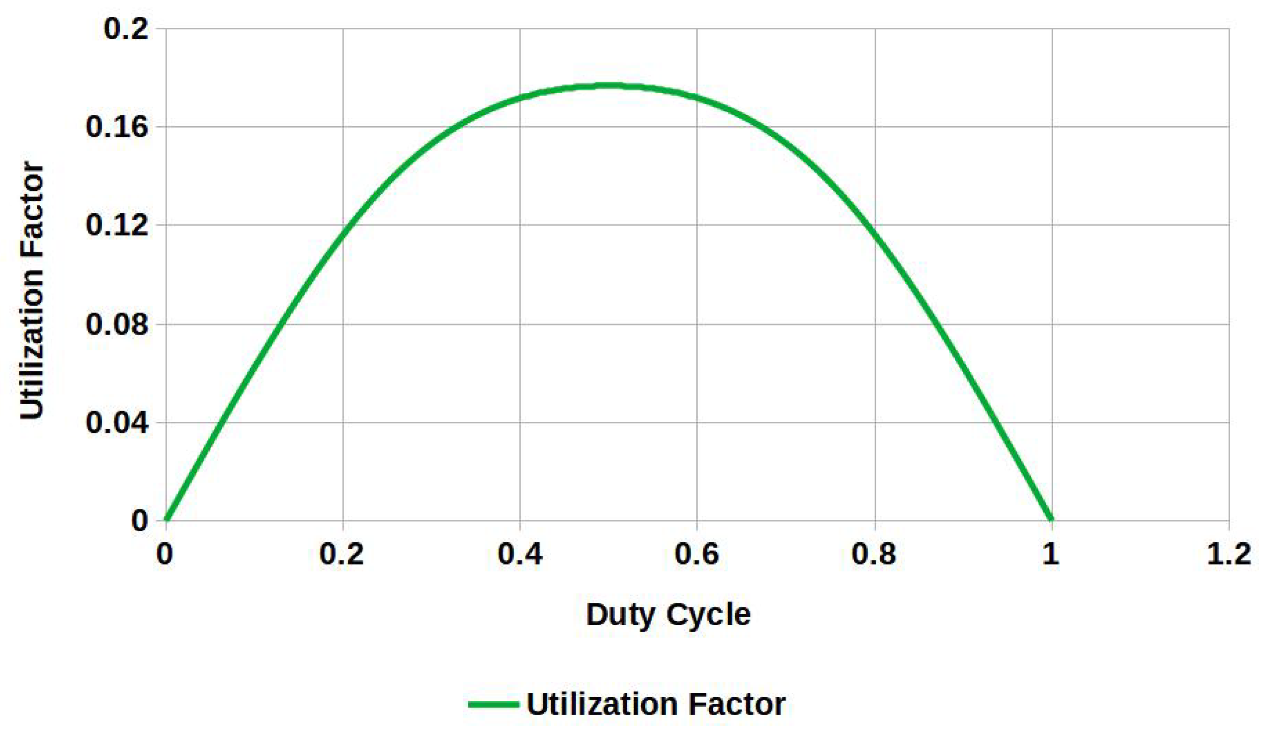
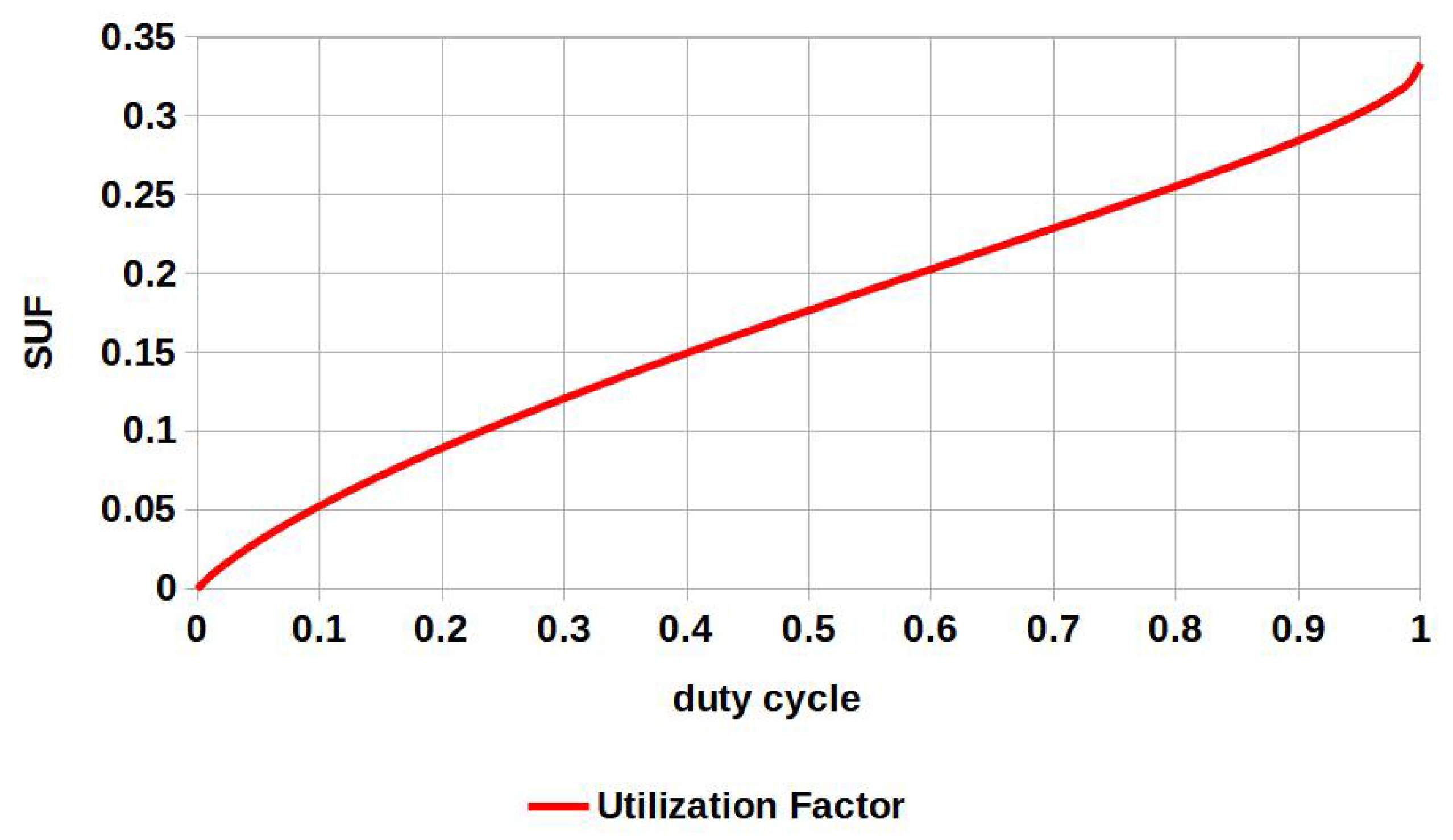
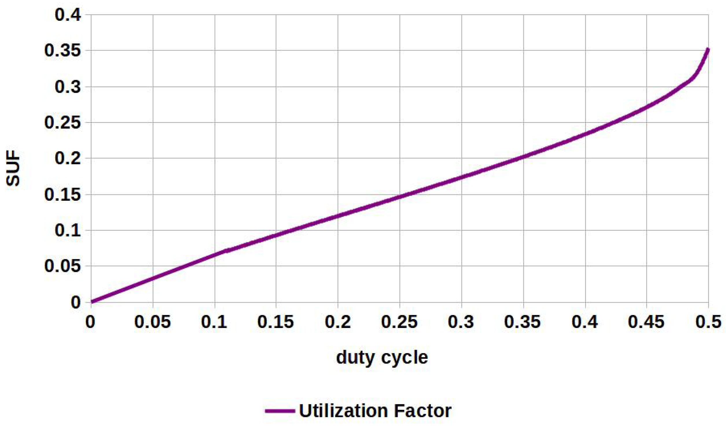
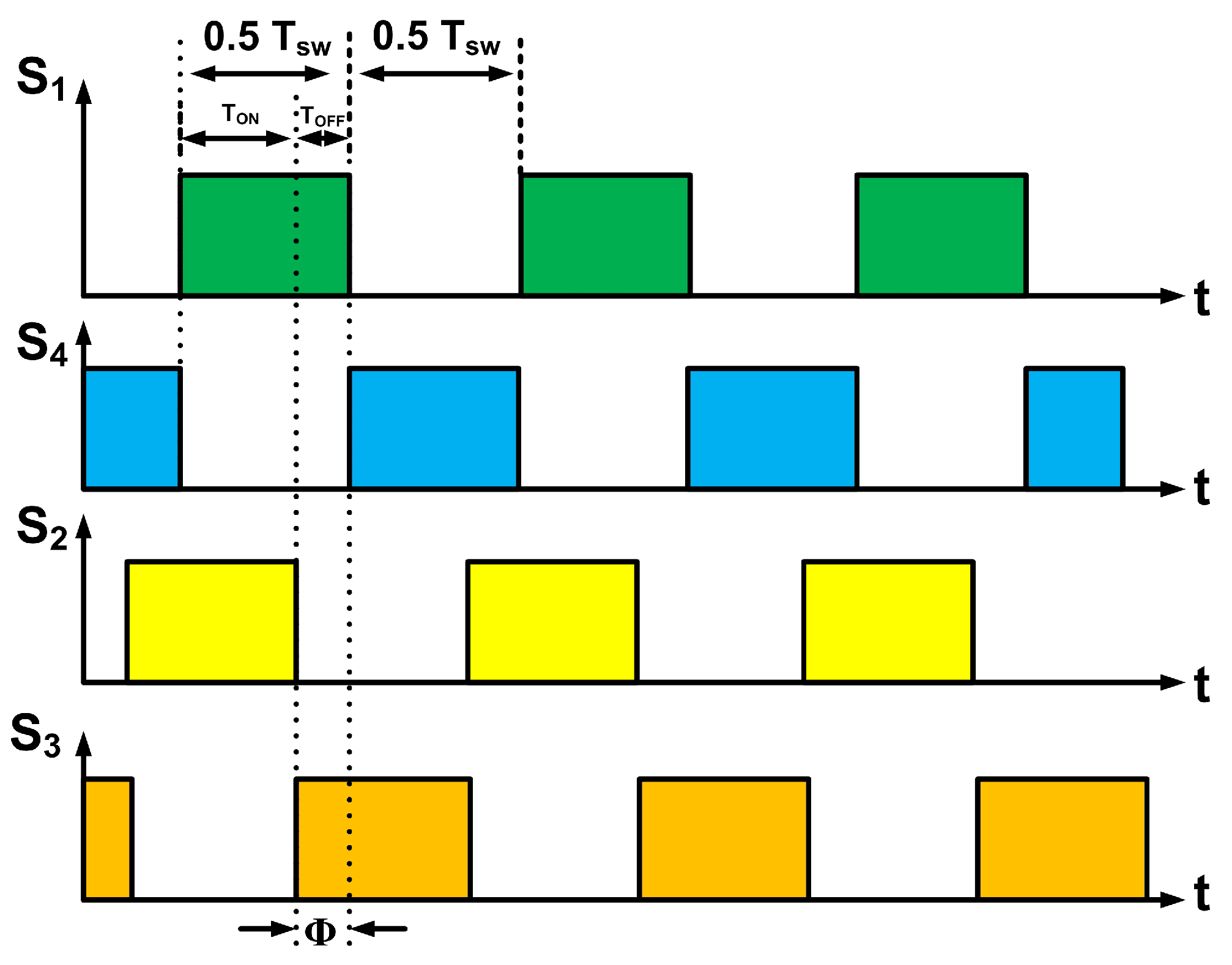
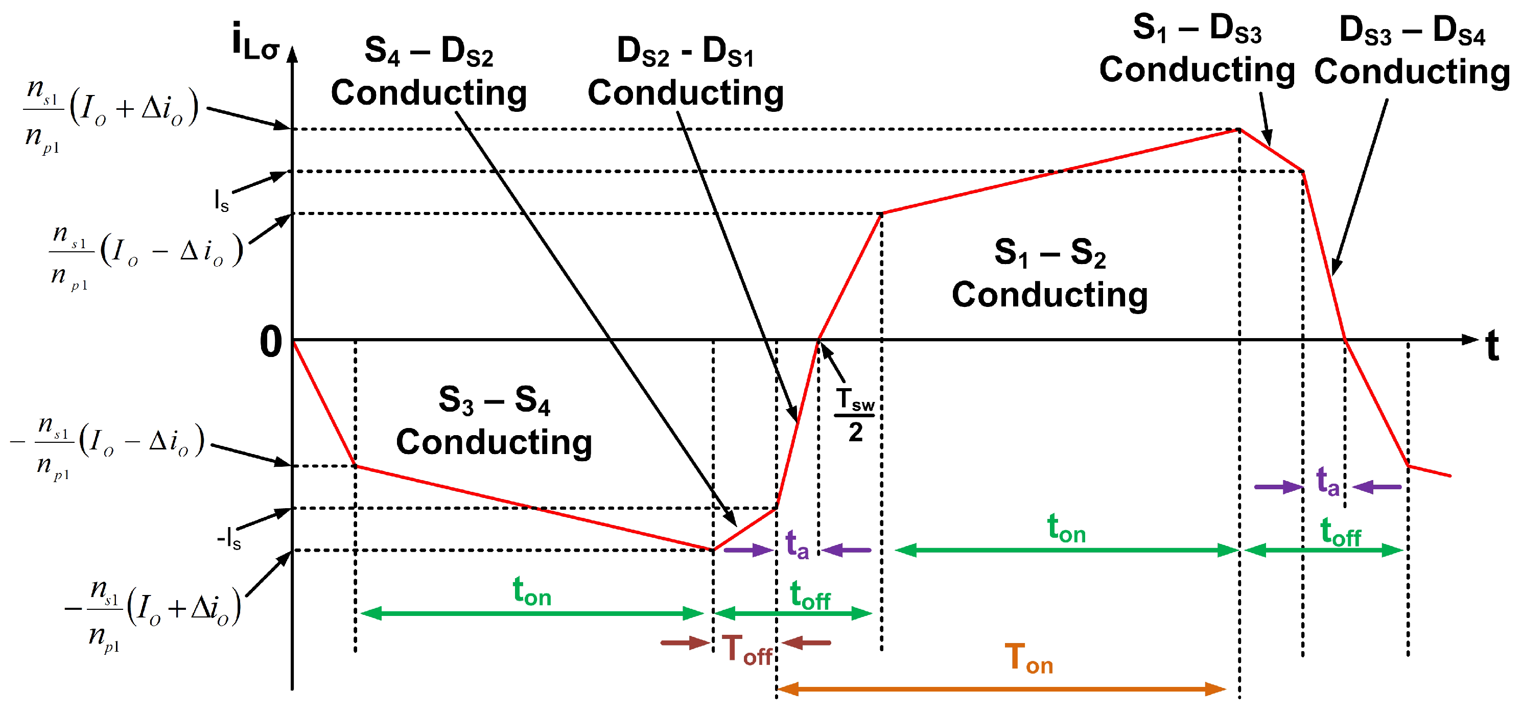
5.4.5. Dual Active Bridge
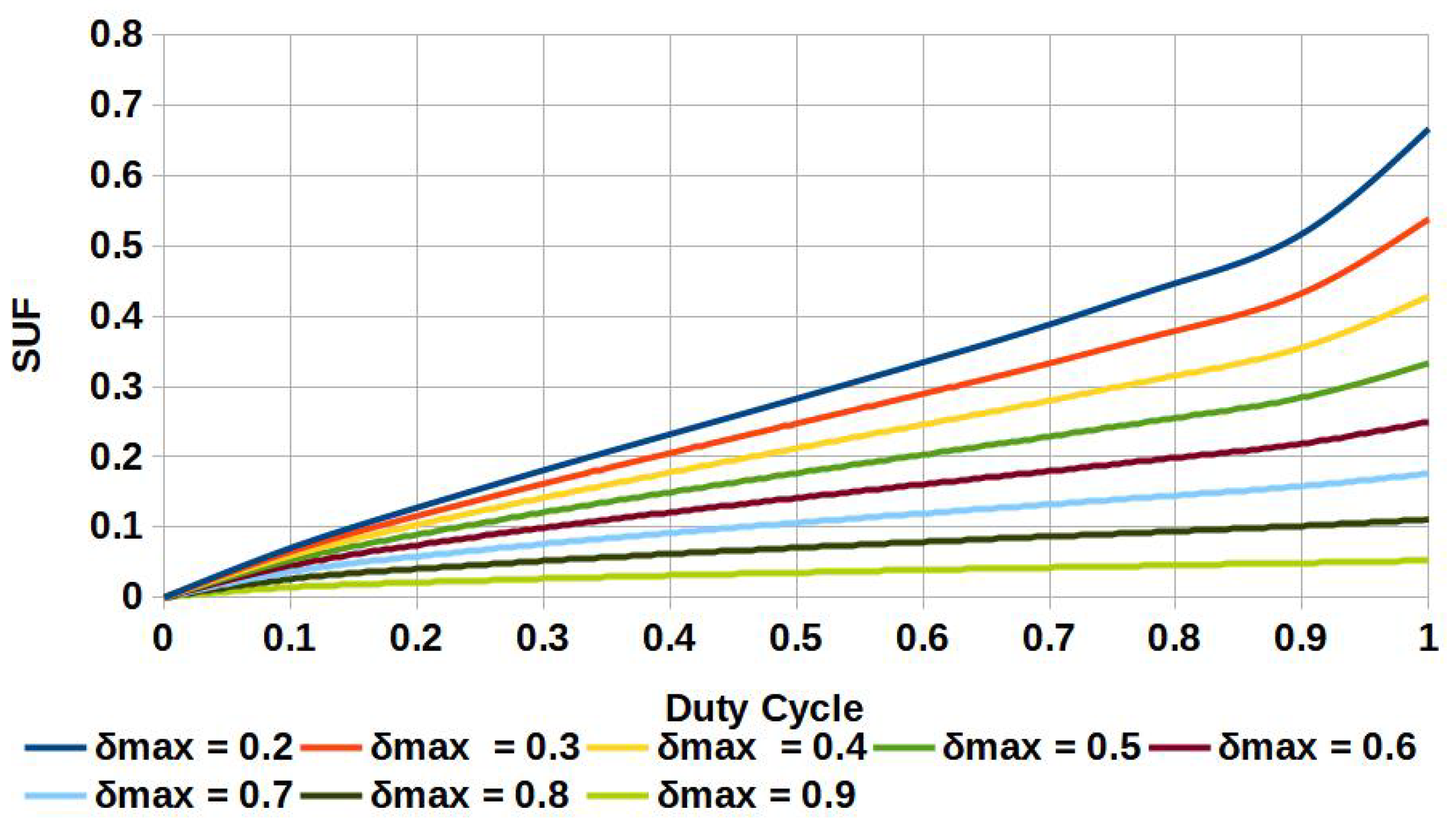
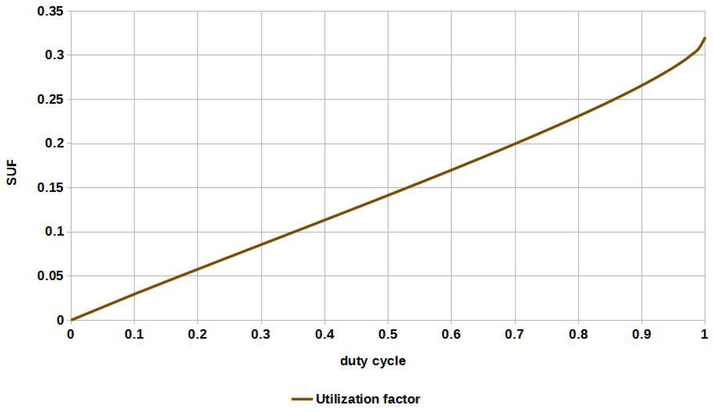
The Dual Active Bridge (DAB) is a bidirectional buck-boost converter. In a DAB, the diodes of the conventional VFFBC are replaced by MOSFET-based H-bridges, as shown in Figure 37. Phase-shifted modulation technique with pulses shown in Figure 38 is generally used for DAB. The corresponding inductor current is shown in Figure 39.
The semiconductor utilization factor ( S U F ) of the DAB is a function of its rated power, input and output voltages, input and output bridge MOSFET currents, and their corresponding body diode currents [105]. It is also a function of the phase shift ( ϕ ) of the pulses provided to the switches (Figure 38). By plotting the ϕ vs. S U F waveform and ϕ vs. Output Power, we can conclude the following:
  • S U F is the best at phase- shifts of 0 and 180 ;
  • However, at these points of phase-shift, the converter is underutilized (output power is close to zero);
  • Hence, despite the low S U F , it is preferred to generate pulses with a phase shift of 90 to maximize power transfer.
For the calculation of power losses, it is to be noted that the losses in the input side MOSFETs are the same as they carry the same current. This argument is valid with the body diodes and the output side MOSFETs. Hence, power loss is estimated from S 1 , S 5 , D S 1 , and D S 5 from Equations (142), (143), (144) and (145), respectively.
P c o n d , S 1 = V t h i 1 2 ϕ 2 π t a T s w + i 1 + i m a x 4 1 ϕ π + r D S , O N 3 i 1 2 ϕ 2 π t a T s w + ( i 1 2 + i m a x i 1 + i m a x 2 ) 1 2 ϕ 2 π
P c o n d , S 1 = V t h i 1 2 n p 1 n s 1 ϕ 2 π t a T s w + r D S , O N 3 i 1 n p 1 n s 1 2 ϕ 2 π t a T s w
P c o n d , D S 1 = V t h i m a x 2 t a T s w + r D S , O N i m a x 2 t a 3 T s w
P c o n d , D S 5 = V t h n p 1 n s 1 i m a x 2 t a T s w + i 1 + i m a x 4 1 ϕ π + r D S , O N 3 c T s w + r D S , O N 3 n p 1 n s 1 2 · ( i 1 2 + i m a x i 1 + i m a x 2 ) 1 2 ϕ 2 π + i m a x 2 t a T s w
The phase-shifted DAB’s main advantage is that the MOSFETs operate under zero voltage switching, and the body diodes operate under zero current switching conditions. Therefore, the losses are reduced, and the efficiency is very high, usually above 95%. Therefore, turn-ON power losses of the MOSFETs and the turn-OFF losses of the body diodes need not be considered. Thus, the switching losses in the MOSFETs S 1 and S 5 are given by Equations (146) and (147), respectively.
P s w , S 1 = ( V i n Δ v C i n ) T s w V 100 F I T w o f f , S 1 i m a x 2 + x o f f , S 1 i m a x + y o f f , S 1
P s w , S 5 = ( V O Δ v C O ) T s w V 100 F I T · w o f f , S 5 i 1 n p 1 n s 1 2 + x o f f , S 1 i 1 n p 1 n s 1 + y o f f , S 1
The DAB topology is well suited for high-power charging systems, fast-charging systems, and systems that charge high-voltage batteries.

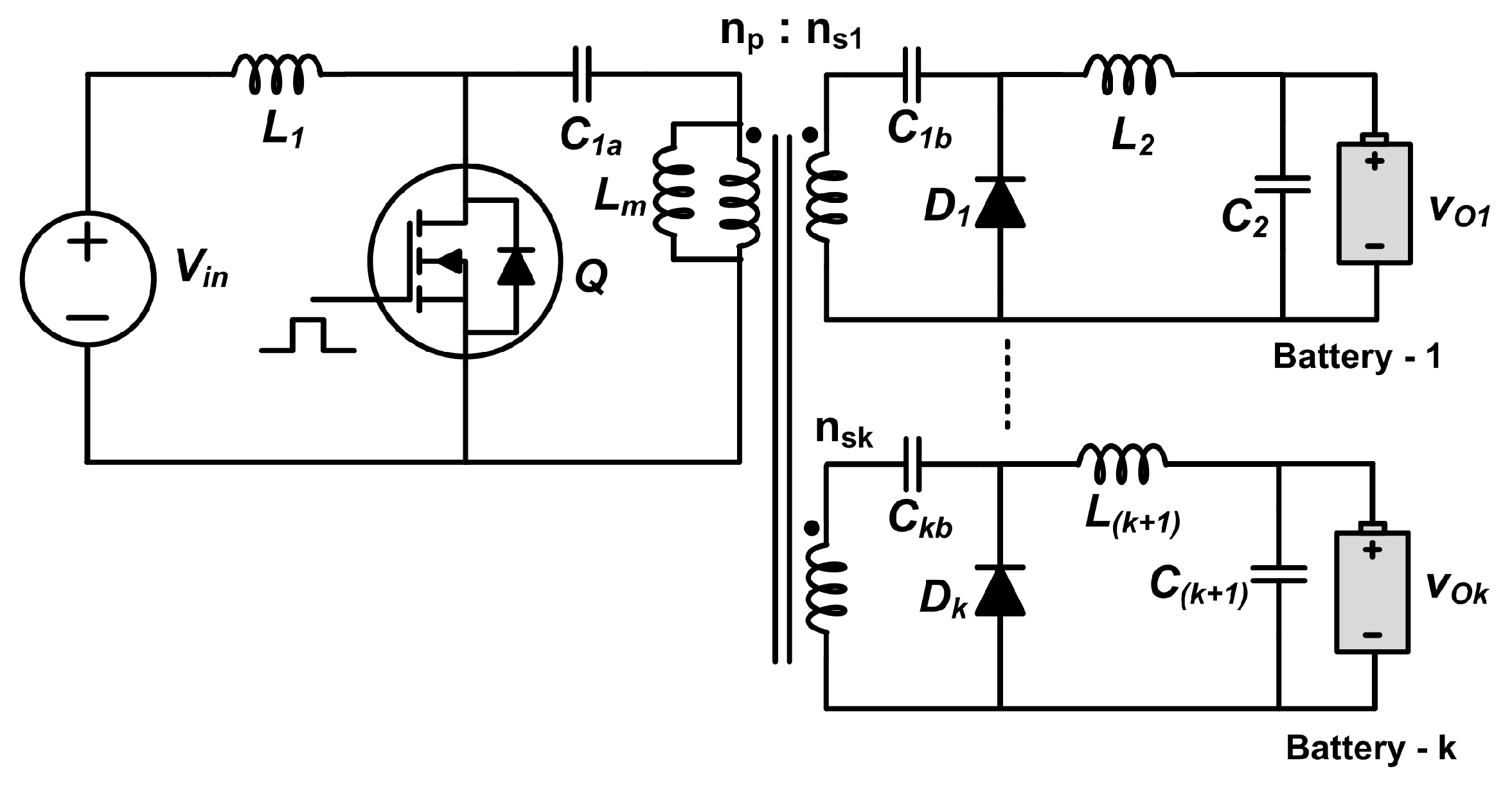
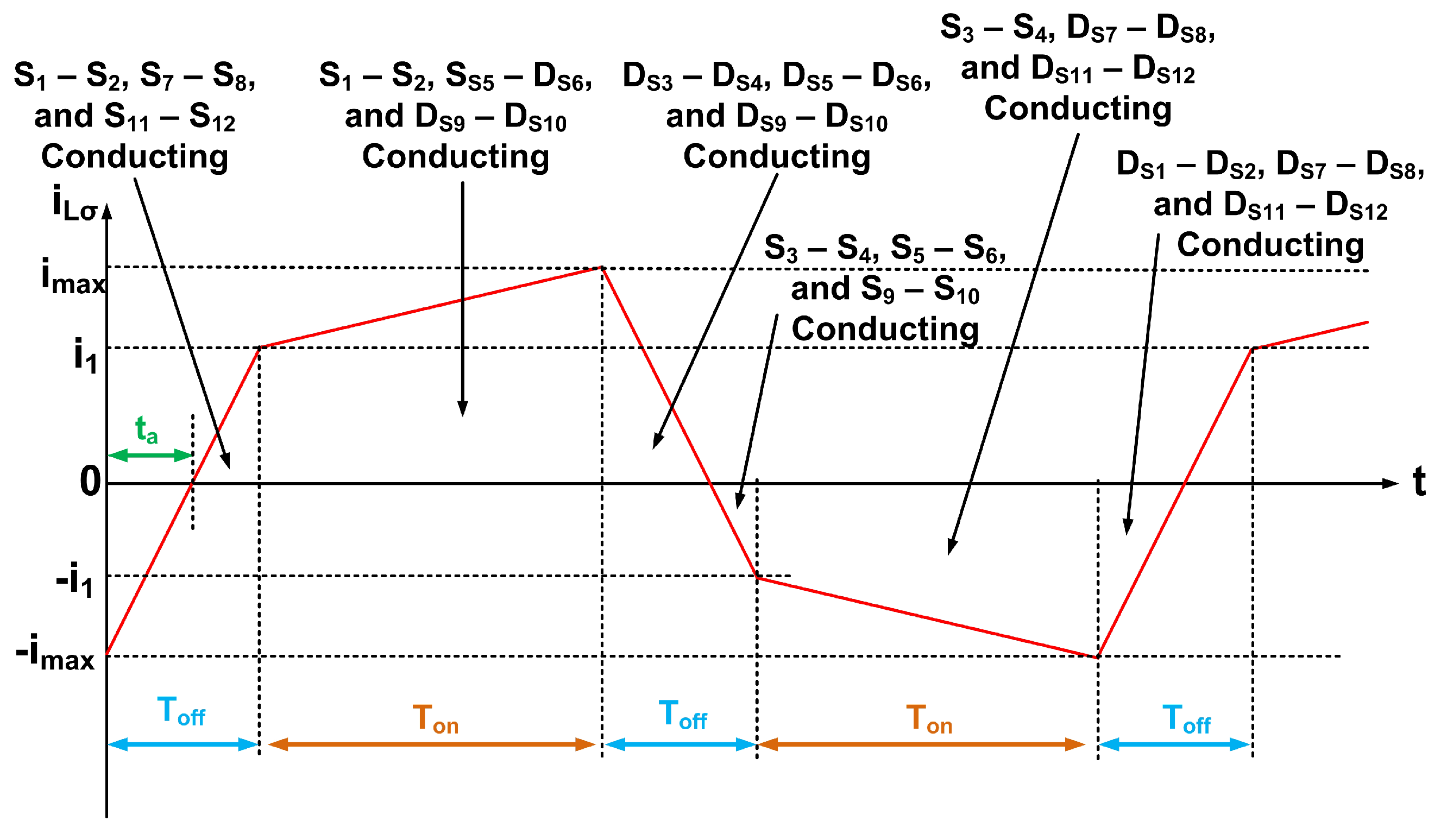
5.5. Isolated DC-DC Resonant Full-Bridge Converters

Resonant converters are the most popular type of isolated DC-DC converters used for high-power battery charging circuits. Among the various types of resonant converters, the two most commonly used types are the LLC resonant converters and CLLC resonant converters. Half-bridge resonant configurations are possible [127], but the power level is limited to medium-power applications. Hence, only full-bridge topologies are considered here.

5.5.1. LLC Resonant Converter

LLC converters are very popular since they can achieve ZVS at the primary and ZCS on the secondary side [128]. It also offers higher power density due to better utilization of the transformer core. The current rating is also less, implying a cost reduction. The LLC-type resonant converter, sometimes referred to as the Series Resonant Converter (SRC), feeding two batteries, is shown in Figure 40. The system consists of a full-bridge converter whose output is connected to the series combination of a resonant inductor ( L R ) and a resonant capacitor ( C R ) and is terminated to the primary of a high-frequency transformer (HFT) having a magnetizing inductance of L m . The detailed design steps of the LLC resonant converter are given in the Infineon application note [129]. Other works [130,131] have also provided detailed designs and analyses of LLC-type converters. The first step in the design of the LLC Converter is to decide the basic specifications, including the range of input voltage (minimum: Vin,min to maximum: Vin,max, and nominal value: Vin), range of the output voltage (minimum:vO,min to maximum: vO,max, and nominal value: vo), maximum output power (PO,max) and the resonant frequency (fr). The switching frequency (fsw) choice depends on the trade-off between the magnetics of L r , and the gauge, cost, and losses corresponding to the Litz wire. In addition, the maximum value of the switching frequency (fsw,max) is limited by the PWM IC used in the control loop for driving the MOSFETS on the primary side of the HFT. A general rule to limit the switching frequency is f s w ( 2.5 × f r ) [131]. The next step is the selection of the turn ratio of the HFT. The transformer turns ratio (nn) at the resonant frequency is given by Equation (148).
n n = V i n 2 × ( v i n , m i n ) + v A K
where, vAK is the ON-state voltage across the diode of the bridge rectifier on the secondary. Next, the minimum value of resonant inductor is calculated using Equation (149) and that of the resonant capacitor is calculated using Equation (150).
L r = n n × V i n × v O 8 × P O × f s w , m a x
C r = 1 ( 2 × π × f r ) 2 × L r
With these values calculated, the characteristic impedance (Zc), the equivalent load and rectifier resistance (Req,ac), and the minimum quality factor (Qmin) are calculated using Equations (151), (152) and (153), respectively.
Z c = L r C r
R e q , a c = 8 × n n 2 π 2 · v O , m a x 2 P O
Q m i n = Z c R e q , a c
The next value to be obtained is the magnetizing inductance of the transformer. To obtain maximum gain at minimum switching frequency [131], the maximum magnetizing inductance (Lm,max) is calculated using Equation (154).
L m , m a x = L r · π 2 4 · f r f s w , m a x 1 1 1 M d c , m a x
where Mdc,max is the maximum DC gain. In addition to this, another magnetizing inductance for zero voltage switching at no-load condition (Lm,ZVS) is calculated using Equation (155).
L m , Z V S = t d × n n × v O , m i n × 1 4 × f s w , m a x t d 2 C s t a r y × V i n , m a x
where t d is the dead time between the pulses, and C s t r a y is the sum of the stray capacitance of the PCB, MOSFETs, and inter-winding capacitance of the transformer and inductor. The final value of the magnetizing inductance is chosen as L m = min( L m , m a x , L m , Z V S ). The verification of the choice of total inductance must satisfy the energy balance given by Equations (156) and (157).
1 2 · L m , m i n + L r I m , p k 2 > 1 2 · C s t r a y · V i n , m a x
I m , p k = n n × V O , m i n 4 × L m × f s w
Deng et al. [130] have used a slightly modified design approach to obtain two different resonant frequencies. Infineon [129] has employed a different approach by calculating the quality factor and gain and then using the same to calculate the resonant component values. Once the values of the resonant components are calculated, the MOSFETs and diodes must be carefully selected. The MOSFETs used in the primary side bridge must be selected based on the current, on-state resistance, dv/dt limits, and reverse recovery time in addition to the output parasitic capacitance value [132]. The selection of the resonant inductor depends on its core type, geometry, and current. Metallized Polypropylene (MKP) capacitors are preferred for resonant capacitors due to higher temperature tolerance, lower cost, and low effective series resistance (ESR). Its selection mainly depends on the current through and the peak voltage across it. For the secondary side bridge, Schottky diodes are preferred due to their low forward voltage drop. Ultrafast diodes can also be chosen for the diode bridge. The resonant components and transformers in multiple numbers are required for charging multiple batteries simultaneously, along with diodes, as shown in Figure 40. If a capacitor is used in the transformer’s secondary, the primary and secondary resonant capacitor values can be equal [133]. If two batteries of different voltage ratings are to be charged, then the resonant component values of the two primaries will be different and need to be calculated separately. Suppose a transformer with one primary and two secondaries is used (instead of two separate transformers) to charge two batteries. In that case, the design values of the resonant components need to be changed by considering the energy increase on the primary side. The main limitation of the LLC resonant converter is the reduced efficiency and loss of ZCS when the converter is operated away from the resonant frequency [133]. The LLC topology is well suited for high-power charging systems, fast-charging systems, and systems that charge high-voltage batteries.

5.5.2. CLLC Resonant Converter

The CLLC type converter is an extension of the LLC resonant converter. It uses one inductor and one capacitor connected in series at the primary and secondary windings. A CLLC converter feeding two batteries is shown in Figure 41.
The design of the CLLC resonant tank is based on the LLC resonant tank described in the previous subsection. The range of input and output voltages and the output power are considered as the defined specifications to begin the design [134]. The transformer turns ratio is calculated using Equation (158), where e is the line voltage variation allowed. Next, the minimum and maximum values of the gain (Mmin and Mmax, respectively) are calculated using Equations (159) and (160), respectively.
n = V i n × ( 1 + e ) v O , m i n
M m i n = v o u t , m i n × n V i n
M m a x = v o u t , m a x × n V i n
Similar to the LLC converter, the CLLC converter switching frequency selection is an important step. A high switching frequency reduces the size of the resonant components and the stress on the resonant capacitors. However, it leads to higher losses. The switching frequency selection criteria for the CLLC converter are the same as that of the LLC converter. The maximum value of the magnetizing inductance (Lm,max) is decided based on the dead-time and the output capacitance (Coss) of the MOSFET. It is calculated using Equation (161).
L m , m a x = t d 16 × f r × C o s s
The primary series resonant inductor (LRP) is calculated using the normalized inductance value (Ln). If Ln is small, a larger voltage gain can be obtained, but the circulating currents will be higher. On the other hand, a large value of Ln will reduce power losses, but the operating frequency range will be wide to meet the required gain. Thus, a trade-off is done to find the value of LRP.
L n = L m L R P
Next, the primary series resonant capacitor (CRP) is calculated using the resonant frequency according to Equation (163). If the DC gain does not match, the value of Lm needs to be adjusted, and the calculation of LRP and CRP needs to be revised.
f r = 1 2 × π L R P × C R P
The series resonant capacitor on the secondary (CRS) needs to be selected based on four parameters. The details of the same are given in [134]. Firstly, a new parameter (Ld) is defined as the ratio of the frequency at the load-independent point to the resonant frequency. To ensure that the frequency at the load-independent point is close to the resonant frequency, a higher value of CRS is preferred.
L d = f l o a d , i n d e p e n d e n t f r
In addition, the selected capacitance should satisfy the gain range. Thus, the value of the capacitance is limited by the gain requirement. The peak gain is to be selected such that it is above the maximum gain requirement. This corresponds to the minimum value of CRS. Based on these, the capacitance CRS is calculated, and the gain is rechecked. Proper tuning of CRS is essential for proper gain output. A similar method of design is given in Refs. [135,136]. A circuit-parameter-based design method is proposed and used in Ref. [137] for CLLC converter design. Ammar et al. [138] have used Equations (165) through (169) to calculate the resonant tank values.
L R P = Q l , m a x × R r , m a x 2 × π × f r
C R P = 1 2 × π × f r × Q l , m a x × R r , m a x
L R S = L R P n 2
C R S = C R P × n 2
L m = k × L R P
where n is the transformer turns ratio, k is the normalized switching frequency, Rload is the load resistance Rr reflected at the rectifier input and referred to the primary side, given by Equation (170), and Q l , m a x is the maximum value of the loaded quality factor, and its nominal value defined by Equation (171).
R r = 2 × n 2 × R l o a d π 2
Q l = L R P C R P R r
The CLLC topology is also well suited for high-power charging systems, fast-charging systems, and systems that charge high-voltage batteries.

5.5.3. LLC and CLLC DAB

Resonant DAB converters are popular due to their high-efficiency, high-power, and high power-density [128]. The LLC and CLLC DAB circuits are shown in Figure 42 and Figure 43, respectively. Texas Instruments design guide [128] details the CLLC DAB converter used for EV chargers. The design of LLC and CLLC DAB resonant components is similar to those described in the previous subsections.
A comparison of the various converters described in Section 5 is given in Table 2, where SS is the soft switching possibility, N L is the number of inductors, N C is the number of capacitors, N s w is the number of switches, and N d i o is the number of diodes.
The DAB topology with an integrated resonant tank is well suited for high-power charging systems, fast-charging systems, and systems that charge high-voltage batteries.

6. High Frequency Transformers in Isolated Converters for Simultaneous Charging

6.1. Relationship Between Switching Frequency and Magnetic Component Size

Isolated converters can be used for higher-wattage systems with the proper design of magnetic components. If the size of the system is a significant concern (especially with magnetic components), wide band-gap (WBG) devices such as SiC and GaN devices can be used. The WBG devices can operate at very high frequencies, SiC in hundreds of kHz and GaN up to MHz, leading to a drastic reduction in the size of magnetic components. Figure 44 shows a sample of two inductors, one being a line frequency (50 Hz) inductor and the other being a high-frequency inductor, having the same inductance value. The size difference is evident from this.
For any magnetic component, the product of the window area and core area (AwAc) is inversely proportional to the switching frequency (fsw) [152] and follows the relationship expressed by Equation (172).
A w A c = P O × J k t × B m a x × f s w
where PO is the output power in W, J is the current density in mA, fsw is in Hz, and kt is the constant whose value is given by,
k t = 0.00100 for   Push - Pull   Converter 0.00140 for   Half - Bridge   Converter 0.00140 for   Full - Bridge   Converter 0.00050 for   Forward   Converter 0.00033 for   Single - Winding   Flyback   Converter 0.00025 for   Multi - Winding   Flyback   Converter
Increasing the frequency leads to an increased skin effect. This implies an increase in the losses due to the AC resistance and an increased temperature. To reduce the skin effect, a smaller diameter wire (skin depth d equal to half the wire diameter) must be chosen while ensuring that the wire can carry the required current. Another method to reduce the skin effect is to use multiple strands of wire, also known as Litz wire. The skin depth can be calculated using Equation (173).
d = k M f s w
where k M is the copper constant whose value varies between 7.5 (at 100 C) and 6.6 (at 20 C). Along with the skin effect, the proximity effect also exists in inductors and transformers. The use of Litz wire also helps in reducing the proximity effect. In addition to these effects, one should evaluate the relationship between the peak-to-peak ripple current ( Δ i L ) and switching frequency. As the switching frequency increases, the inductance value should be proportionately reduced to keep the peak-peak ripple current within the required limits. For example, if a 100 μ H existing inductor operates at 200 kHz, and if the frequency is increased to 400 kHz, the inductance should be reduced by 53 μ H (standard inductance value) [152]. This is necessitated either due to the frequency roll-off characteristic of the core material or due to the self-resonance between the winding inductance and its self-capacitance [153]. Core loss is another component that varies with frequency. To prevent core losses from increasing when the frequency is increased, the flux density must be maintained constant. The response of most high-frequency power inductors varies only a little for a large range of frequencies [153]. Generally, testing is performed at a standard frequency of 100 kHz.

6.2. Transformers with Multiple Secondary Windings

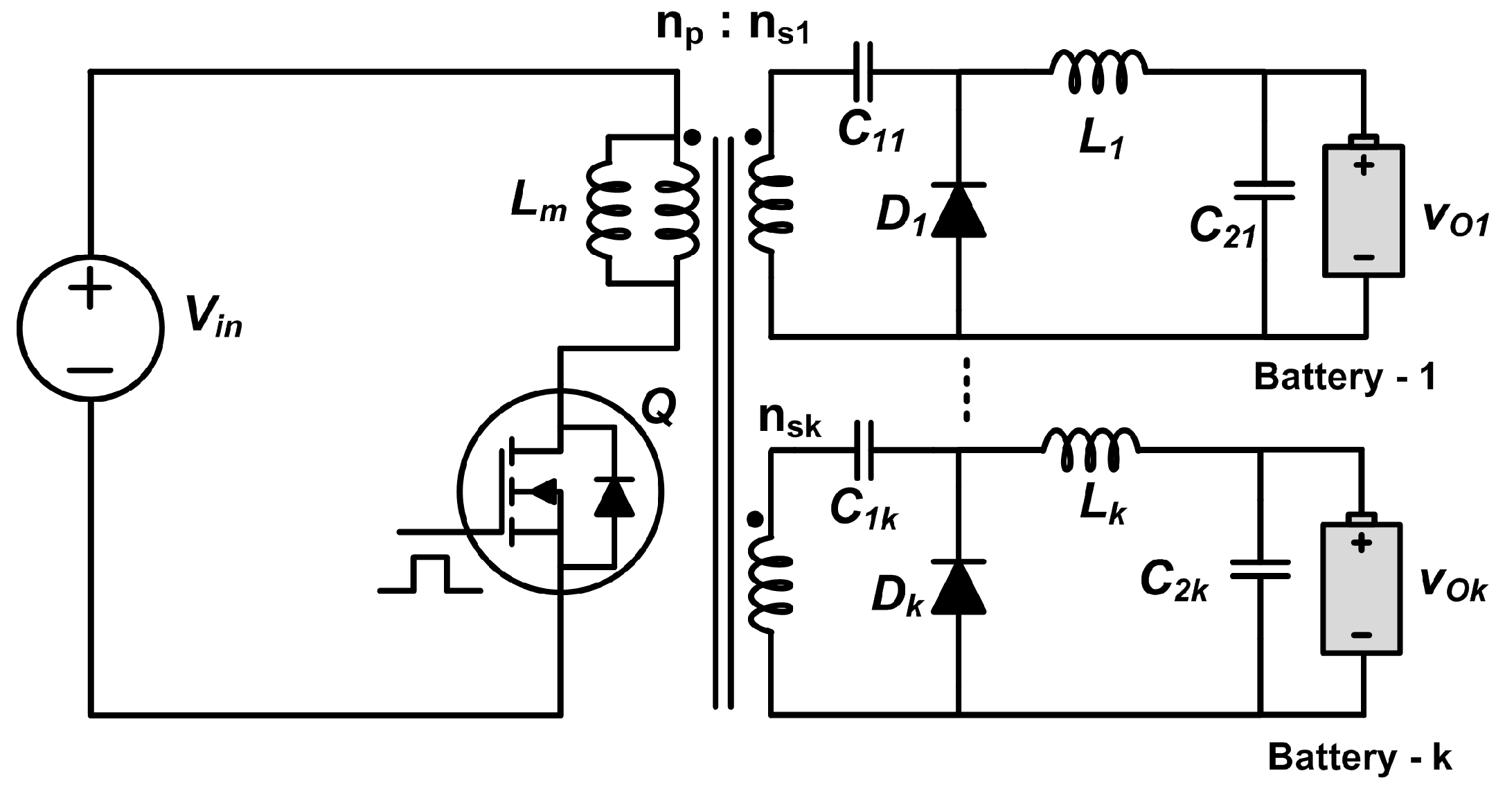
6.2.1. Transformers with One-Primary and Multiple-Secondary Windings

The converters in the preceding sections need one or more transformers with ‘k’ number of secondary windings. Therefore, it is necessary to design such a transformer. The window area allocated for each winding wound on the ferrite core depends on the power handling capability of each secondary. Such a transformer is shown in Figure 45a. It has one primary winding and two secondary windings. Each winding takes a fraction of the total window area (Aw). This fraction is denoted as ‘k’ for the kth winding [154] and is given by Equation (174).
k = A k A w
where Ak represents the winding area of the kth winding. If a wire of length lk is used for the kth winding, then the wire resistance Rk will be calculated using Equation (175).
R k = l k A wk
where Awk represents the area of wire used in the kth winding. It is obtained from the wire gauge table. The total number of turns of the kth winding ( n k ) will be inversely proportional to Awk and the actual length of the wire based on parameter α k (fractional area of the total winding area) will be estimated using Equation (176).
l k n k × ( M L T ) K
where MLT is the mean length per turn of the wire. The new resistance can then be calculated by taking the wire fill factor (ku = 0.3 for Litz wire and 0.9 for foil), as,
R k = n k 2 × ( M L T ) k W A × k u
For detailed and generic analysis of magnetics for power converters, works [155,156,157] can be referred to. The detailed design of transformers with multiple secondaries is out of the scope of this review. Ref. [154] explains in detail the design and analysis of the transformer with single primary and multiple secondary windings.

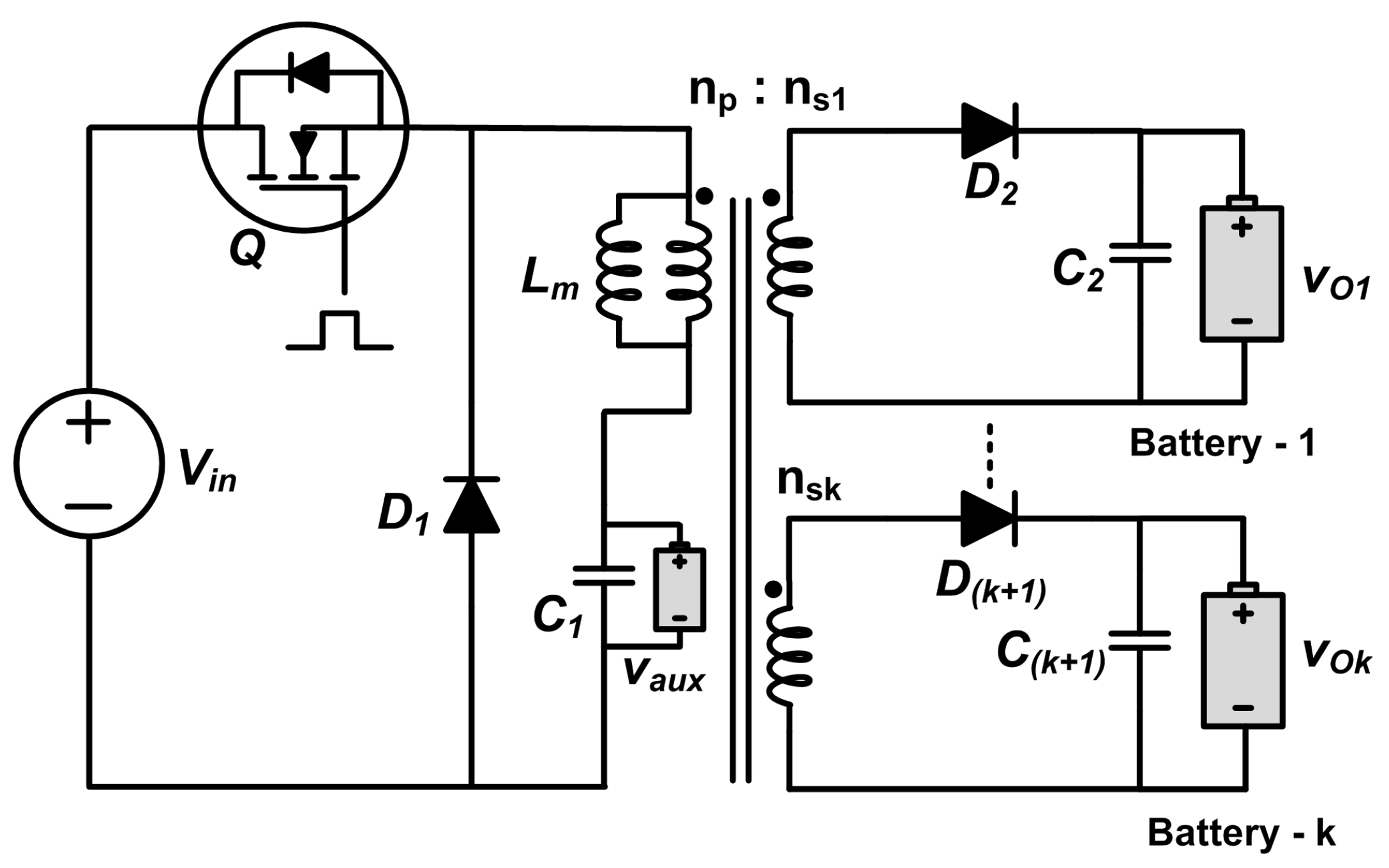
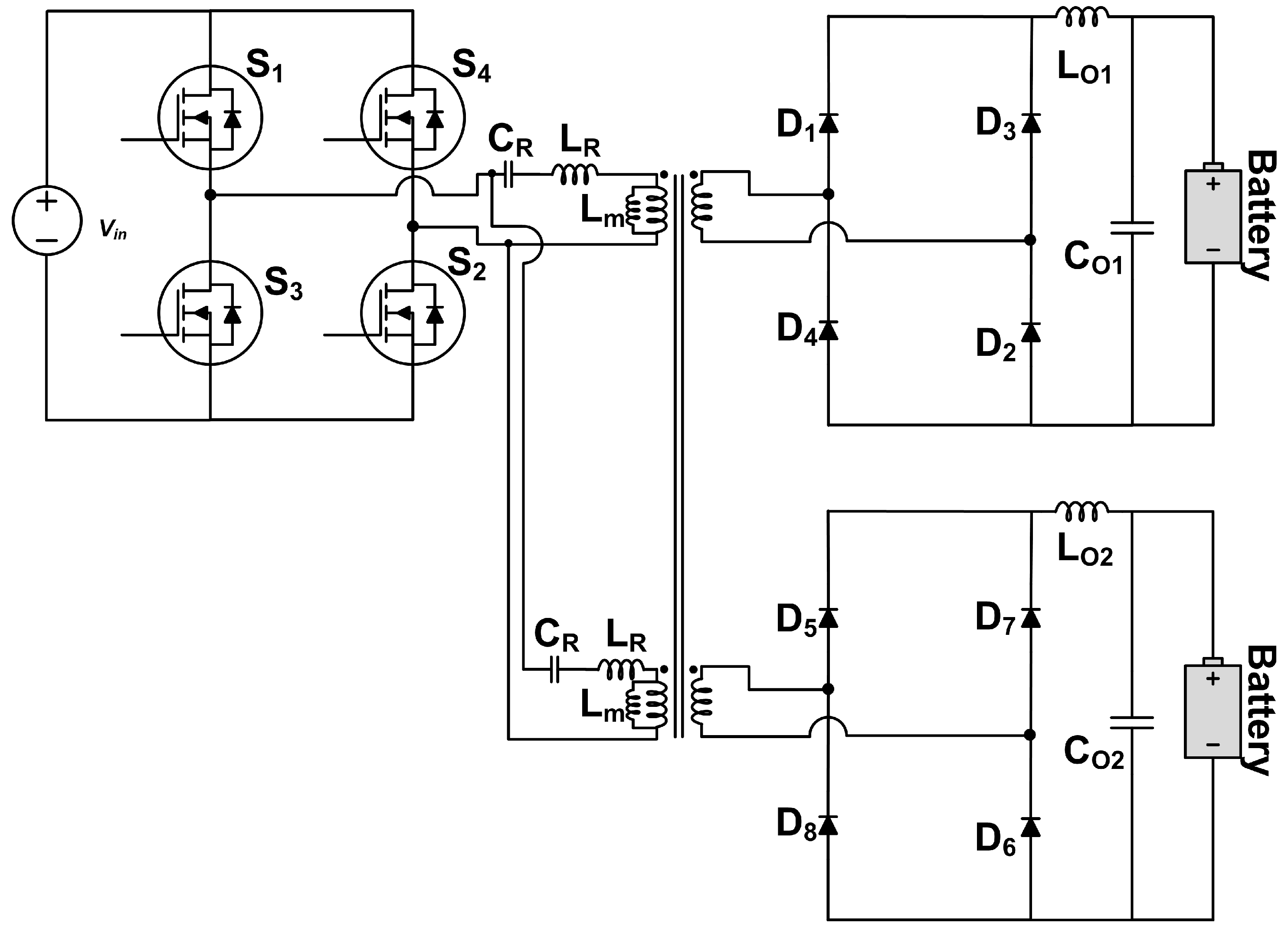
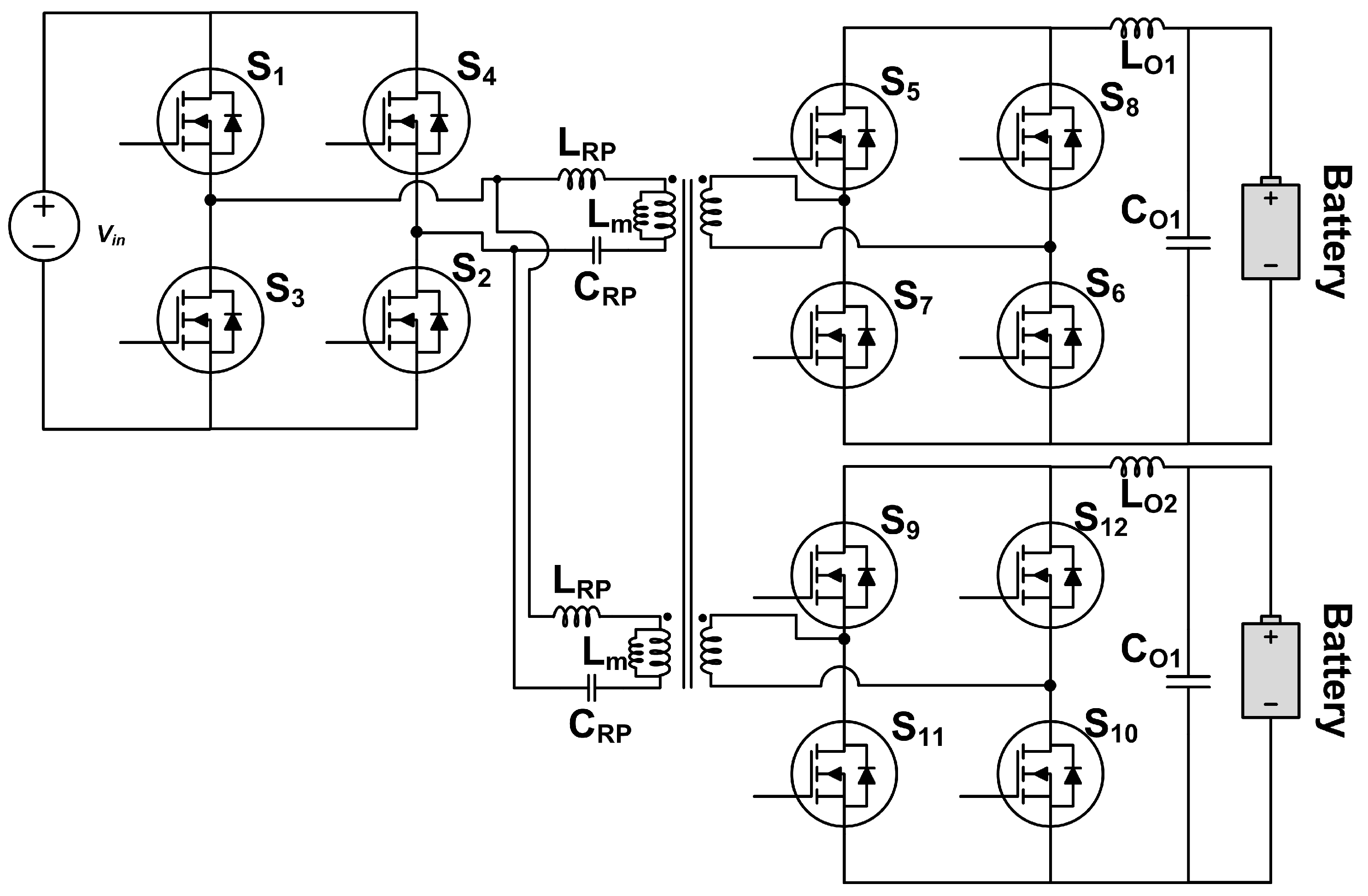
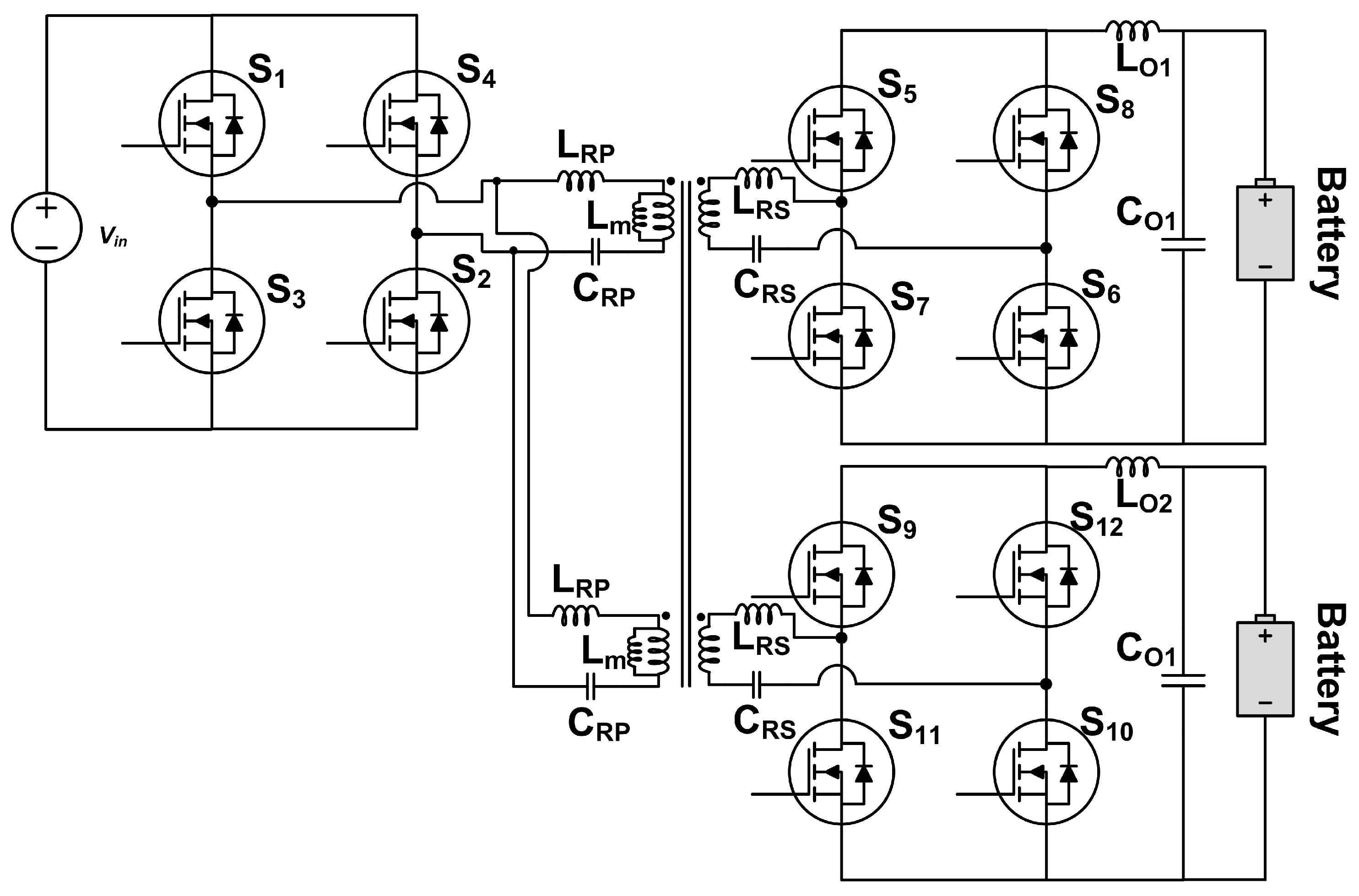
6.2.2. Use of Multiple Transformers to Obtain Equivalent Transformer with Multiple Secondary Windings

If a transformer described in the previous subsection is unavailable, there is another way to obtain the same effect. If two separate transformers are available, then the primaries of both transformers can be connected in parallel to obtain an equivalent transformer with two isolated secondaries. This is shown in Figure 45b.
Using a single transformer with multiple secondaries has advantages such as lesser space requirement and relatively smaller size. It weighs less than the setup with multiple transformers with their primaries in parallel. On the other hand, if a setup with multiple primary windings is used, each transformer can have a different turns ratio based on availability (e.g., n p 1 : n s 1 = 1:2 and n p 2 : n s 2 = 2:3), thereby enabling charging batteries of different voltage ratings. Based on the availability and other constraints, either type can be used in the converters employed to charge multiple batteries.

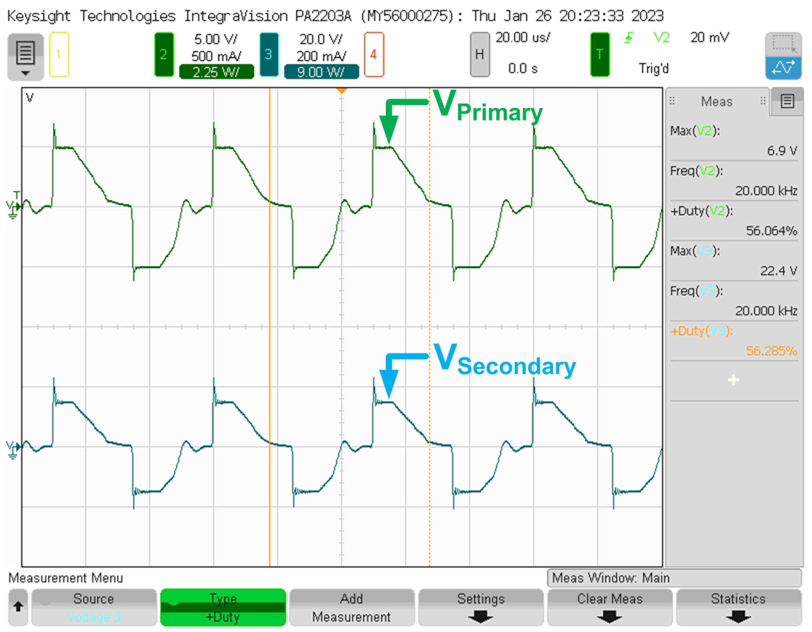
6.3. Testing of High-Frequency Transformers Used in Isolated DC-DC Converters

All the isolated DC-DC Converters use high-frequency transformers. However, researchers and engineers should focus on the following critical points.
  • The transformer response must be checked for square wave input before it is connected to any converter;
  • The transformer response for step-up and step-down operations must be checked.
The response check is vital because the voltage input to the transformer in any DC-DC converter is a square wave, not a sinusoidal wave. Even in resonant converters such as full bridge LLC and CLLC types, the voltage is a square while the current is sinusoidal. The response of the transformer can be quite different when square wave voltage input is given to it instead of sinusoidal input. The testing needs to be done for both sides since a confirmation regarding the quality of the response is required for both step-up and step-down operations. It is customary to assume that a step-up transformer works as a step-down transformer if the supply and load terminals are interchanged. However, the frequency range needs to be verified before connecting it as a part of any converter. A basic step-by-step procedure for high-frequency transformer response testing suggested by the authors based on their research and testing experience is as follows:
  • Connect the square wave input source (signal generator) terminals to the transformer’s primary;
  • Keeping the transformer on no-load, connect the positive and negative terminals of the probe (from the scope where the waveform needs to be seen) to the secondary terminals;
  • Set a frequency in the input source;
  • After checking the transformer ratio (step up or step down, and the peak value of the voltage increase or decrease), provide the square wave signal of appropriate magnitude from the source;
  • Observe the response on the scope;
  • Change the frequency of the input signal and observe the waveform again;
  • Repeat the steps for various frequencies and obtain the range of frequencies for which the transformer gives the best response. The transformer under test (TUT) should be used only in that frequency range to obtain the best response and efficiency;
  • Now, interchange the supply and scope terminals (primary to secondary and secondary to primary) and repeat the steps to obtain the frequency range for this operation.
A setup to perform such testing is shown in Figure 46. The square wave is provided from the Digilent Analog Discovery 2 processor using its ‘Wavegen’ mode, and the response is seen in the Keysight IntegraVision Power Analyzer PA2203A. In the waveforms shown in Figures to, V P r i m a r y represents the voltage across the primary winding, and V S e c o n d a r y represents the voltage across the seconday winding of the transformer.
Figure 47 shows the input (5 V, 20 kHz square wave) given to the primary windings of the 100 V, 40 A/300 V, 12 A high-frequency transformer, and the output voltage across the secondary. In the output waveform, a slope can be seen. The waveform pattern indicates that the square wave input does not give square wave output, which is unacceptable in a converter. Hence the TUT is not suitable for operation at that switching frequency (20 kHz here). It is seen that the input wave also gets distorted at the frequencies at which the transformer is not magnetically compatible to work.
Figure 48 show the 5 V, 100 kHz square wave input, and the output voltage. It is observed here that the output pattern is very close to that of a square wave, implying that the TUT works well at this frequency (100 kHz here).
Similar tests were performed by providing the input to the terminals labeled ‘secondary’ and output voltage measured across the terminals labeled ‘primary’. This is done to check the operational frequency range of the transformer for the operation when the primary and secondary terminals are interchanged. Figure 49 shows the waveforms for a 50 kHz signal applied to the secondary winding and its response across the primary winding.
Similarly, when a 100 kHz square wave was provided to the secondary and the response was measured across the primary, the input and the corresponding response obtained are shown in Figure 50.
Similar tests can be performed for this combination, and the range of frequencies can be noted. For the TUT shown in Figure 46, the test was carried out, and the range of frequencies for the step-down operation was found to be between 60 kHz and 270 kHz, while the range for step-up operation of the same transformer was found to be between 45 kHz and 295 kHz. It can be seen from Figure 47 and Figure 49 that even the voltage across the primary gets distorted when operated at low frequencies, even when a square wave with no disturbance is applied across it. Since the magnetic circuit does not give a proper response at that frequency, the secondary voltage gets distorted and reflects on the primary side. This needs to be noted before the HFT is used in any converter.

7. High-Voltage Batteries in Electric Vehicles

The EV charging systems in passenger vehicles could be classified into two main types [158] based on the battery voltage levels. The systems which operate in the voltage range of 150 to 450 V are called the 400 V system. Some vehicles in this range include the Audi e-Tron (396 V), Mercedes Benz (EQC-405 V, EQA and EQB-420 V), Nissan Leaf (350 V), Tesla S (400 V), Volkswagen (e-Up-374 V) [159] among others. High-end vehicles such as Porsche Taycan (800 V), Aston Martin Rapide E (800 V), and Kia EV6 (697 V) [159] in which the battery voltage can reach up to 850 V, come under the 800 V system. With the use of 800 V systems, there are multiple benefits, especially related to fast charging. With the use of an 800 V system, the size of the cables can be reduced, along with the reduction in conduction losses, lower cooling requirement (relative to the 400 V systems), and smaller motor and wire gauge due to lower currents [160].
Jung et al. [158] have described the benefits of higher voltage batteries when used in EVs. The article discusses the technical constraints, EV layout and design changes, their standardization, corresponding connectors, and their relation to fast charging. The article concludes by describing the advantages customers get due to the upgradation of battery voltages. Aghabali et al. [160] have provided a detailed review of the 800 V vehicle systems for EV batteries, along with the various challenges and future trends of the system in commercial use. The researchers have analyzed the performance of the system based on the battery pack, the cables used (for conventional and fast charging), BMS, the protection system and the clearance requirements, considering the Tesla Model 3 and Porsche Taycan Turbo S vehicles which use the 400 V and 800 V battery packs, respectively. The thermal concerns and risk evaluation with the partial discharge of battery packs have been considered in this work. On the inverter side, the required configurations for the 400 V and 800 V systems have been detailed with case studies, current calculations, and loss analysis. For the auxiliary power unit (APU), the full-bridge converter with soft switching, DAB, and full-bridge with current doubler are considered for the 400 V system. At the same time, a modular structure is proposed for the 800 V system. Charger configuration has been provided for the 400 V and 800 V EVs, and the future trends have been explained.
Grazian et al. [159] have proposed a voltage/current doubler circuit for inductive wireless power transfer for 400 V and 800 V battery applications. The authors have provided the modeling, component selection, analysis, and economics details. Hardware results have been provided by considering a 7.7 kW prototype with bidirectional power supplies. The performance analysis for coil misalignment and coil distance, with the loss analysis, has been provided. Efficiency greater than 95% has been obtained for all test cases in the work. Among the isolated converters described in the preceding sections, the full-bridge topology, phase-shifted full bridge, and resonant topologies are best suited for 400 V and 800 V battery charging applications.

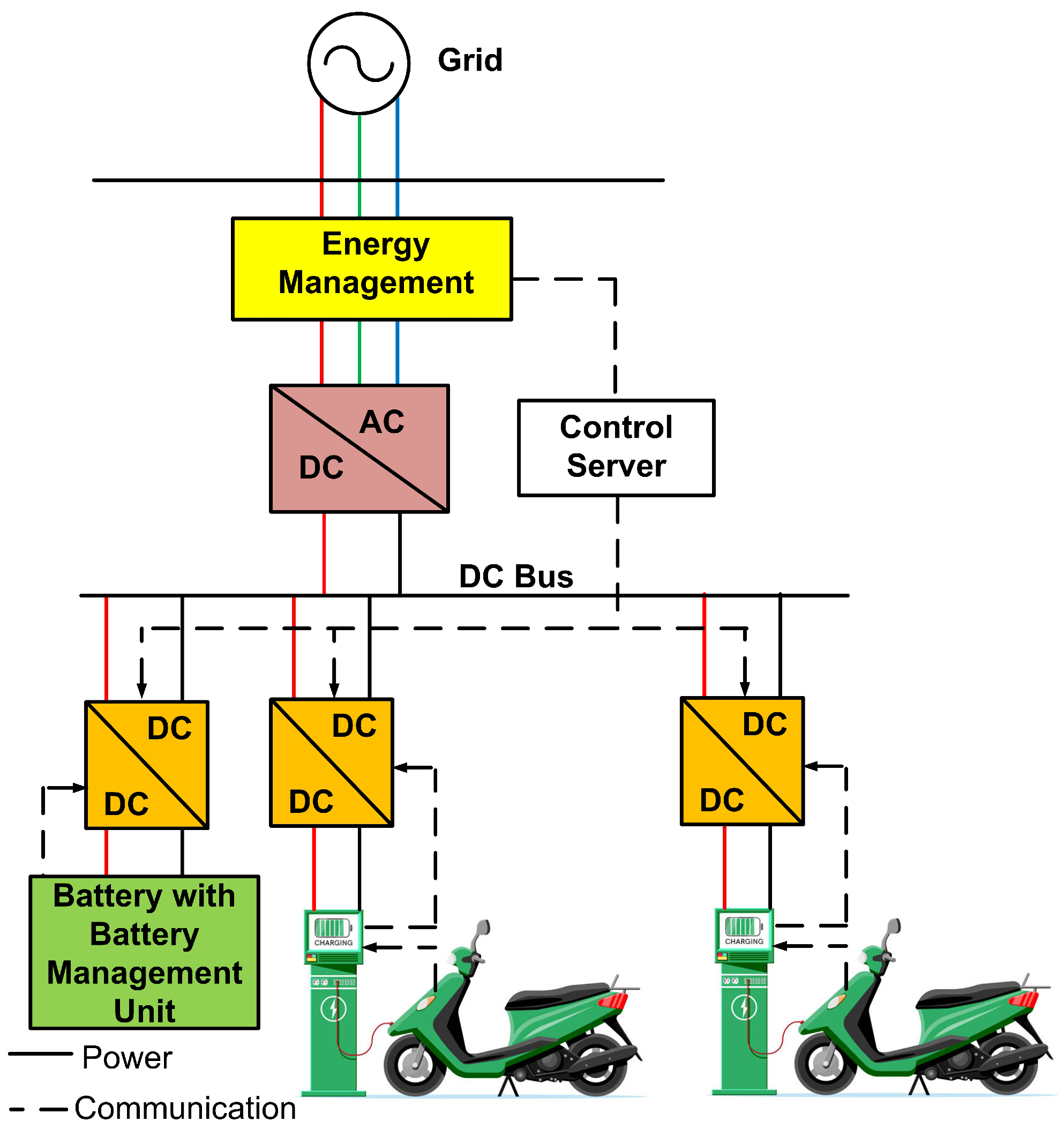
8. Simultaneous Charging Feature: Implementation in Products and Public Projects

ABB has launched a charger called “Terra 360” [161], which is a high-power charger that supports the combined charging system (CCS, up to 360 kW), CHAdeMO (up to 150 kW) and AC type-2 (up to 22 kW) charging protocols. The DC output voltage ranges from 200 V to 920 V. It provides two DC outputs and two more options for DC outputs, thus enabling the simultaneous charging of four vehicles of different ratings.
Electric Vehicle Energy Storage Company (EVESCO) has launched its “EVDC-60NA” charger [162] of the EVDC series, which has the capability of charging two EVs at a time. The system can supply a DC power of 60 kW with 200 to 1000 V output. The rated input is three-phase 480 V, 60 Hz AC. It has an inbuilt AC-DC converter and supports both CCS and CHAdeMO protocols.
Volkswagen has created a pilot project in Saxony [163] where a mega power bank has been assembled using EV batteries that are no longer suitable for use in EVs. In this pilot project, up to eight vehicles can be charged simultaneously with a total output of 75 kW. The source is a 570 kWh capacity solar panel installed on the site.
Proterra’s Proterra 1440 kW Charging System [164] is a large fleet solution custom-built to charge 24 vehicles simultaneously and up to 48 vehicles sequentially. It works on a 480 V, 60 Hz AC input at a power factor greater than 0.99 and a total harmonic distortion of less than 3 % . The maximum continuous DC current is 200 A with an optional extension to 300 A based on the vehicle limitation. The DC output voltage is a large-range output between 150 V and 1000 V.
The United States Transportation Department (USDOT) has proposed the installation of fast chargers that can charge four vehicles simultaneously, with each port having a capacity of 150 kW or higher [165]. The total budget allotted for the proposed project is around USD 5 billion.
ČEZ public fast chargers at Vestec, Central Bohemia, were tested under a complete islanding operation for two hours [166] to charge 12 Renault ZOE EVs simultaneously. The system used a PV source with a capacity of 20 kW and a battery bank with a capacity of 275 kWh. The ENET VŠB Centre-Technical University of Ostrava, the Brno University of Technology and ABB supported the project.
City Charger from Delta [167] is a 100 kW EV fast charging system that supports simultaneous charging outputs with a feature that can optimize the charging rate during simultaneous charging. It supports CCS and CHAdeMO protocols and operates from a 480 V, 50 Hz AC input at a power factor of 0.99 with an efficiency greater than 94 % at full-load. The current THD satisfies the IEEE 519 standards.
The Firmer Electric DC charging system [168] is a combined charging system with AC and DC charging features that can charge three vehicles simultaneously. It can dynamically distribute power optimally to all EVs. The maximum power capacity is 150 kW for the DC side and 43 kW for the AC side.
While all the products/projects described in Section 8 boast the feature of simultaneous charging, no specific details have been provided in the corresponding references regarding the number and type of converters used in each charging system and their components. By simultaneous charging, if the implication is the installation of ‘k’ number of charging systems to charge ‘k’ batteries, the system can technically charge multiple batteries. However, the waiting time will still be high. This scenario should not be confused with the case where multiple batteries can be charged from one charger, the latter case being more beneficial than the former from the standpoint of reduction of waiting time.

9. Future Scope of Simultaneous Charging

The future of Electric Vehicles is bright. In this regard, the importance of simultaneous charging cannot be overstated. Whether the EV charging systems deployment involves grid-connected or grid-independent systems, the scope is seemingly endless.
  • The source side challenges involve integrating fuel cells, solar PV systems, and the grid. Some research has been conducted in this regard, but the implementation is yet to be done at the product level for mass use. The development of optimized source combinations for slow and fast charging by integrating conventional and renewable energy sources is to be taken to reduce the dependency on conventional sources;
  • With the addition of renewable sources, the intermittency of power availability needs to be addressed. This poses a significant challenge when grid independence is an objective. Efficient storage systems need to be integrated to ensure round-the-clock power availability.
On the converter topology side, some of the research possibilities include the following:
  • Optimizing existing topologies to reduce the system’s size, weight, and the cost is a significant research problem. While research works have proposed several new converters, those topologies have yet to reach implementation level in actual chargers. This gap has to be bridged by optimizing the converter in terms of topology and performance;
  • With the advent of SiC and GaN devices, the converters can be switched at very high frequencies, reducing the size of magnetic components and reducing passive component losses. The design of appropriate gate driver circuits for SiC and GaN MOSFETs and protection circuits for these devices is a significant research area with tremendous untapped potential. The design of proper driving circuits will directly affect the switching characteristics of the devices, thereby affecting the losses;
  • Optimization of the layout of PCB with the use of SiC and GaN devices with proper clearances is another area that has to be addressed. This will be very critical with the implementation of a simultaneous charging feature;
  • With HV batteries, topologies used at these voltages must be developed and optimized for fast and ultra-fast charging.
On the converter control side, some of the research possibilities include the following:
  • Universal control techniques optimized specifically for battery charging must be developed and implemented for standard power levels;
  • Newer techniques that involve deep neural networks and fuzzy-neural systems need to be employed to make the charger more intelligent.
In addition to these changes, one can look into ways of encouraging the widespread use of EVs. For this, it is necessary to reduce the waiting time and charging time, along with deploying sufficient charging systems. This implies that future research should deal with fast and ultra-fast charging methods and simultaneous charging topologies to address the time-related concerns. One should look into the possibility of deploying more charging systems to address the possibility of increasing the number of chargers. Another emerging field for research in simultaneous charging is wireless charging systems.
  • Deployment of WPT systems, specifically dynamic charging systems, can be revolutionary. Dynamic charging eliminates the requirement of parking and plugging-in of vehicles for charging and the associated wiring system. In addition, the range anxiety of the users can be reduced since charging can be done on the go;
  • The two main challenges with wireless power transfer include relatively lower efficiency and coil separation distance limitation. This needs to be addressed by researchers to enable mass use;
  • Another modification that can be made is to use LLC and CLLC type converters (full-bridge variants or DAB) with wireless coils instead of transformers. This will ensure ZVS and ZCS operation, leading to higher efficiency;
  • If this can be extended to multiple-output chargers to charge multiple batteries of the same or different ratings simultaneously, then a further boost is provided to the implementation.
It can be concluded that the implementation of simultaneous charging of EVs will lead to a greener and cleaner earth (Figure 51), and easier and faster charging with lower waiting times, which will lead to an overall increase in EV usage.

10. Conclusions

This article has presented the state of the art of simultaneously charging batteries for EV applications. The review has given details of the charging methods, various charging techniques, standards, and charging levels for EV batteries. The specifications of commercial chargers are presented for both AC and DC charging. Primary concerns related to power quality with battery charging have been reviewed in this paper. The state of the art of simultaneous charging of EV batteries has been presented to enable the researchers to implement newer topologies for the application. Several existing topologies of isolated DC-DC converters that can be extended to implement simultaneous charging have been presented with the related design and loss estimation equations. The extensions include single-switch, two-switch, and bridge-type isolated DC-DC converters, which are suitable for charging EV batteries that need power at different levels and charging at different speeds limited by the batteries. The suitability of these converters for EV battery charging has been described to enable a better choice.
A testing method for HFTs has been provided to enable researchers to decide the frequency range at which the TUT performs well. The recent advancement in the use of HV batteries in EVs has been explained with the advantages and details of several EVs in the market that use HV batteries. The future scope of simultaneous charging has been detailed for the benefit of the readers to help guide the next phase of research in the domain.
It can be seen from the review that resonant and phase-shifted full-bridge converters are best suited for high-power, high-voltage battery charging, and fast charging. Single-switch and two-switch topologies can be used for low- and medium-power EV charging, essential in charging stations that implement simultaneous charging. A charging station that implements simultaneous charging should combine low- and high-power compatible converters so that vehicles of different power and voltage ratings can be charged simultaneously. This will drive the majority of future research in EV battery charging. An optimal combination of topologies suitable for low- and high-power EV charging will be the future of research and implementation for EV charging globally.

Author Contributions

Conceptualization, S.B.S. and G.A.; testing, S.B.S. and G.A.; resources, S.B.S. and G.A.; data curation, S.B.S. and G.A.; writing—original draft preparation, S.B.S.; writing—review and editing, S.B.S. and G.A.; visualization, S.B.S.; supervision, G.A.; project administration, G.A. All authors have read and agreed to the published version of the manuscript.

Funding

This research received no external funding.

Institutional Review Board Statement

Not applicable.

Informed Consent Statement

Not applicable.

Data Availability Statement

Not applicable.

Acknowledgments

The transformer testing shown was performed at the DST-FIST Sponsored Smart Grid Setup-PHIL Lab at the School of Electrical Engineering, Vellore Institute of Technology, Vellore.

Conflicts of Interest

The authors declare no conflict of interest.

References

  1. Reitz, R.D.; Ogawa, H.; Payri, R.; Fansler, T.; Kokjohn, S.; Moriyoshi, Y.; Agarwal, A.; Arcoumanis, D.; Assanis, D.; Bae, C.; et al. IJER editorial: The future of the internal combustion engine. Int. J. Engine Res. 2020, 21, 3–10. [Google Scholar] [CrossRef]
  2. Guttikunda, S.K.; Jawahar, P. Atmospheric emissions and pollution from the coal-fired thermal power plants in India. Atmos. Environ. 2014, 92, 449–460. [Google Scholar] [CrossRef]
  3. Holechek, J.L.; Geli, H.M.; Sawalhah, M.N.; Valdez, R. A global assessment: Can renewable energy replace fossil fuels by 2050? Sustainability 2022, 14, 4792. [Google Scholar] [CrossRef]
  4. Höök, M.; Tang, X. Depletion of fossil fuels and anthropogenic climate change—A review. Energy Policy 2013, 52, 797–809. [Google Scholar] [CrossRef]
  5. Botelho, A.; Ferreira, P.; Lima, F.; Pinto, L.M.C.; Sousa, S. Assessment of the environmental impacts associated with hydropower. Renew. Sustain. Energy Rev. 2017, 70, 896–904. [Google Scholar] [CrossRef]
  6. Singh, A.; Singha, N. Environmental impact of nuclear power: Law and policy measures in India. Humanit. Soc. Sci. Rev. 2016, 4, 88–95. [Google Scholar] [CrossRef]
  7. Nasr Esfahani, F.; Darwish, A.; Williams, B.W. Power converter topologies for grid-tied solar photovoltaic (PV) powered electric vehicles (EVs)—A comprehensive review. Energies 2022, 15, 4648. [Google Scholar] [CrossRef]
  8. Jin, C.; Sheng, X.; Ghosh, P. Optimized electric vehicle charging with intermittent renewable energy sources. IEEE J. Sel. Top. Signal Process. 2014, 8, 1063–1072. [Google Scholar] [CrossRef]
  9. Al-Shahri, O.A.; Ismail, F.B.; Hannan, M.; Lipu, M.H.; Al-Shetwi, A.Q.; Begum, R.; Al-Muhsen, N.F.; Soujeri, E. Solar photovoltaic energy optimization methods, challenges and issues: A comprehensive review. J. Clean. Prod. 2021, 284, 125465. [Google Scholar] [CrossRef]
  10. Notter, D.A.; Gauch, M.; Widmer, R.; Wager, P.; Stamp, A.; Zah, R.; Althaus, H.J. Contribution of Li-ion batteries to the environmental impact of electric vehicles. Environ. Sci. Technol. 2010, 44, 6550–6556. [Google Scholar] [CrossRef]
  11. Yu, X.; Li, W.; Gupta, V.; Gao, H.; Tran, D.; Sarwar, S.; Chen, Z. Current Challenges in Efficient Lithium-Ion Batteries’ Recycling: A Perspective. Glob. Challenges 2022, 6, 2200099. [Google Scholar] [CrossRef]
  12. Dalala, Z.M.; Alnawafa, M.; Saadeh, O.; Alnawafa, E. Reducing commuter CO2 footprint through transit PV electrification. Sustainability 2020, 12, 6406. [Google Scholar] [CrossRef]
  13. Aziz, M.; Oda, T. Simultaneous quick-charging system for electric vehicle. Energy Procedia 2017, 142, 1811–1816. [Google Scholar] [CrossRef]
  14. Shahjalal, M.; Shams, T.; Tasnim, M.N.; Ahmed, M.R.; Ahsan, M.; Haider, J. A critical review on charging technologies of electric vehicles. Energies 2022, 15, 8239. [Google Scholar] [CrossRef]
  15. Guo, S.; Han, Z.; Wei, J.; Guo, S.; Ma, L. A Novel DC-AC Fast Charging Technology for Lithium-Ion Power Battery at Low-Temperatures. Sustainability 2022, 14, 6544. [Google Scholar] [CrossRef]
  16. Shadnam Zarbil, M.; Vahedi, A.; Azizi Moghaddam, H.; Khlyupin, P.A. Design and Sizing of Electric Bus Flash Charger Based on a Flywheel Energy Storage System: A Case Study. Energies 2022, 15, 8032. [Google Scholar] [CrossRef]
  17. Switch-Mode, Linear, and Pulse Charging Techniques for Li+ Battery in Mobile Phones and PDAs. Available online: https://www.analog.com/en/technical-articles/switchmode-linear-and-pulse-charging-techniques-for-li-battery-in-mobile-phones-and-pdas.html (accessed on 15 November 2022).
  18. Vermeer, W.; Stecca, M.; Mouli, G.R.C.; Bauer, P. A Critical Review on The Effects of Pulse Charging of Li-ion Batteries. In Proceedings of the 2021 IEEE 19th International Power Electronics and Motion Control Conference (PEMC), Gliwice, Poland, 25–29 April 2021; pp. 217–224. [Google Scholar] [CrossRef]
  19. Huang, X.; Li, Y.; Acharya, A.B.; Sui, X.; Meng, J.; Teodorescu, R.; Stroe, D.I. A review of pulsed current technique for lithium-ion batteries. Energies 2020, 13, 2458. [Google Scholar] [CrossRef]
  20. Khan, A.B.; Pham, V.L.; Nguyen, T.T.; Choi, W. Multistage constant-current charging method for Li-ion batteries. In Proceedings of the 2016 IEEE Transportation Electrification Conference and Expo, Asia-Pacific (ITEC Asia-Pacific), Busan, Republic of Korea, 1–4 June 2016; pp. 381–385. [Google Scholar]
  21. Liu, P.J.; Chen, T.F.; Yang, H.S. A Li-Ion Battery Charger with Variable Charging Current and Automatic Voltage-Compensation Controls for Parallel Charging. IEEE J. Emerg. Sel. Top. Power Electron. 2021, 10, 997–1006. [Google Scholar] [CrossRef]
  22. Notten, P.H.; het Veld, J.O.; Van Beek, J. Boostcharging Li-ion batteries: A challenging new charging concept. J. Power Sources 2005, 145, 89–94. [Google Scholar] [CrossRef]
  23. Tomaszewska, A.; Chu, Z.; Feng, X.; O’kane, S.; Liu, X.; Chen, J.; Ji, C.; Endler, E.; Li, R.; Liu, L.; et al. Lithium-ion battery fast charging: A review. ETransportation 2019, 1, 100011. [Google Scholar] [CrossRef]
  24. Faria, J.P.; Velho, R.L.; Calado, M.R.; Pombo, J.A.; Fermeiro, J.B.; Mariano, S.J. A New Charging Algorithm for Li-Ion Battery Packs Based on Artificial Neural Networks. Batteries 2022, 8, 18. [Google Scholar] [CrossRef]
  25. Hemavathi, S.; Shinisha, A. A study on trends and developments in electric vehicle charging technologies. J. Energy Storage 2022, 52, 105013. [Google Scholar] [CrossRef]
  26. Gao, Z.; Ma, B.; Liu, X.; Chen, S.; Xie, H.; Yu, H. Study on Lithium-ion Battery Degradation Caused by Side Reactions in Fast-charging Process. Front. Energy Res. 2022, 10, 905710. [Google Scholar] [CrossRef]
  27. Khalid, A.; Sarwat, A.I. Fast Charging Li-Ion Battery Capacity Fade Prognostic Modeling Using Correlated Parameters’ Decomposition and Recurrent Wavelet Neural Network. In Proceedings of the 2021 IEEE Transportation Electrification Conference & Expo (ITEC), Chicago, IL, USA, 23–25 June 2021; pp. 27–32. [Google Scholar]
  28. Al-Saadi, M.; Olmos, J.; Saez-de Ibarra, A.; Van Mierlo, J.; Berecibar, M. Fast Charging Impact on the Lithium-Ion Batteries’ Lifetime and Cost-Effective Battery Sizing in Heavy-Duty Electric Vehicles Applications. Energies 2022, 15, 1278. [Google Scholar] [CrossRef]
  29. Wang, L.; Qin, Z.; Slangen, T.; Bauer, P.; van Wijk, T. Grid impact of electric vehicle fast charging stations: Trends, standards, issues and mitigation measures-an overview. IEEE Open J. Power Electron. 2021, 2, 56–74. [Google Scholar] [CrossRef]
  30. Rwamurangwa, E.; Gonzalez, J.D.; Butare, A. Integration of EV in the Grid Management: The Grid Behavior in Case of Simultaneous EV Charging-Discharging with the PV Solar Energy Injection. Electricity 2022, 3, 563–585. [Google Scholar] [CrossRef]
  31. Filip, R.; Püvi, V.; Paar, M.; Lehtonen, M. Analyzing the Impact of EV and BESS Deployment on PV Hosting Capacity of Distribution Networks. Energies 2022, 15, 7921. [Google Scholar] [CrossRef]
  32. Alshareef, S.M. Analyzing and Mitigating the Impacts of Integrating Fast-Charging Stations on the Power Quality in Electric Power Distribution Systems. Sustainability 2022, 14, 5595. [Google Scholar] [CrossRef]
  33. Chon, S.; Bhardwaj, M.; Nene, H. Maximizing Power for Level 3 EV Charging Stations. 2018. Available online: https://www.ti.com/lit/wp/sway014/sway014.pdf?ts=1674470563613&ref_url=https%253A%252F%252Fwww.google.com%252F (accessed on 15 November 2022).
  34. Kumar K, J.; Kumar, S.; VS, N. Standards for electric vehicle charging stations in India: A review. Energy Storage 2022, 4, e261. [Google Scholar] [CrossRef]
  35. Nakanishi, T.; Zaitsu, H.; Kikuta, T.; Tsuda, S.; Nii, H. CHAdeMO-Conformity High-Power Charger Connector Assembly for Over 100 kW-Class EV Charge. SEI Tech. Rev. 2019, 88, 49–54. [Google Scholar]
  36. Jaman, S.; Verbrugge, B.; Garcia, O.H.; Abdel-Monem, M.; Oliver, B.; Geury, T.; Hegazy, O. Development and Validation of V2G Technology for Electric Vehicle Chargers Using Combo CCS Type 2 Connector Standards. Energies 2022, 15, 7364. [Google Scholar] [CrossRef]
  37. AC Charger. Eaton xChargeIn Mobility. Available online: https://www.eaton.com/gb/en-gb/catalog/emobility/xchargein-mobility.specifications.html (accessed on 18 December 2022).
  38. DC Charger. Eaton Green Motion DC 22. Available online: https://www.eaton.com/gb/en-gb/catalog/emobility/green-motion-dc-22.specifications.html (accessed on 18 December 2022).
  39. DC Charger. Eaton Green Motion DC 44/66. Available online: https://www.eaton.com/gb/en-gb/catalog/emobility/green-motion-dc-44-66.specifications.html (accessed on 18 December 2022).
  40. DC Charger. Siemens SiCharge. Available online: https://new.siemens.com/global/en/products/energy/medium-voltage/solutions/emobility/sicharge-d.html (accessed on 18 December 2022).
  41. AC Charger. Siemens VersiCharge. Available online: https://new.siemens.com/global/en/products/energy/medium-voltage/solutions/emobility/versicharge.html (accessed on 18 December 2022).
  42. Khalid, M.; Ahmad, F.; Panigrahi, B.K.; Al-Fagih, L. A comprehensive review on advanced charging topologies and methodologies for electric vehicle battery. J. Energy Storage 2022, 53, 105084. [Google Scholar] [CrossRef]
  43. Ghasemi-Marzbali, A. Fast-charging station for electric vehicles, challenges and issues: A comprehensive review. J. Energy Storage 2022, 49, 104136. [Google Scholar]
  44. Chakraborty, S.; Vu, H.N.; Hasan, M.M.; Tran, D.D.; Baghdadi, M.E.; Hegazy, O. DC-DC converter topologies for electric vehicles, plug-in hybrid electric vehicles and fast charging stations: State of the art and future trends. Energies 2019, 12, 1569. [Google Scholar] [CrossRef]
  45. Agamy, M.S.; Harfman-Todorovic, M.; Elasser, A.; Steigerwald, R.L.; Sabate, J.A.; Chi, S.; McCann, A.J.; Zhang, L.; Mueller, F. A high efficiency DC-DC converter topology suitable for distributed large commercial and utility scale PV systems. In Proceedings of the 2012 15th International Power Electronics and Motion Control Conference (EPE/PEMC), Novi Sad, Serbia, 4–6 September 2012; p. LS2d–3. [Google Scholar]
  46. Karmaker, A.K.; Roy, S.; Ahmed, M.R. Analysis of the impact of electric vehicle charging station on power quality issues. In Proceedings of the 2019 International Conference on Electrical, Computer and Communication Engineering (ECCE), Cox’s Bazar, Bangladesh, 7–9 February 2019; pp. 1–6. [Google Scholar]
  47. IEC61000-3-2; Electromagnetic Compatibility (EMC)-Part 3-2: Limits—Limits for Harmonic Current Emissions (Equipment Input Current ≤ 16 A per Phase. IEC Standard: Geneva, Switzerland, 2018; pp. 1000–1003.
  48. Monolithic Power. Power Factor Correction (PFC). Available online: https://www.monolithicpower.com/en/power-factor-correction (accessed on 3 December 2022).
  49. Kolar, J.W.; Friedli, T. The essence of three-phase PFC rectifier systems—Part I. IEEE Trans. Power Electron. 2012, 28, 176–198. [Google Scholar] [CrossRef]
  50. Friedli, T.; Hartmann, M.; Kolar, J.W. The essence of three-phase PFC rectifier systems—Part II. IEEE Trans. Power Electron. 2013, 29, 543–560. [Google Scholar] [CrossRef]
  51. Figueiredo, J.P.M.; Tofoli, F.L.; Silva, B.L.A. A review of single-phase PFC topologies based on the boost converter. In Proceedings of the 2010 9th IEEE/IAS International Conference on Industry Applications-INDUSCON 2010, São Paulo, Brazil, 8–10 November 2010; pp. 1–6. [Google Scholar]
  52. Semiconductor, O. Power Factor Correction Handbook; HBD853/D, Rev; Newark Electronics: Chicago, IL, USA, 2007; Volume 3. [Google Scholar]
  53. Efthymiou, L.; Camuso, G.; Longobardi, G.; Udrea, F.; Lin, E.; Chien, T.; Chen, M. Zero reverse recovery in SiC and GaN Schottky diodes: A comparison. In Proceedings of the 2016 28th International Symposium on Power Semiconductor Devices and ICs (ISPSD), Prague, Czech Republic, 12–16 June 2016; pp. 71–74. [Google Scholar]
  54. Huber, L.; Jang, Y.; Jovanovic, M.M. Performance evaluation of bridgeless PFC boost rectifiers. IEEE Trans. Power Electron. 2008, 23, 1381–1390. [Google Scholar] [CrossRef]
  55. Jang, Y.; Jovanovic, M.M. A bridgeless PFC boost rectifier with optimized magnetic utilization. IEEE Trans. Power Electron. 2009, 24, 85–93. [Google Scholar] [CrossRef]
  56. Sharifi, S.; Monfared, M.; Babaei, M. Ferdowsi rectifiers—Single-phase buck-boost bridgeless PFC rectifiers with low semiconductor count. IEEE Trans. Ind. Electron. 2019, 67, 9206–9214. [Google Scholar] [CrossRef]
  57. Lange, A.D.B.; Soeiro, T.B.; Ortmann, M.S.; Heldwein, M.L. Three-level single-phase bridgeless PFC rectifiers. IEEE Trans. Power Electron. 2014, 30, 2935–2949. [Google Scholar] [CrossRef]
  58. Ge, K.; Liu, Q. Research on dual boost semi-bridgeless PFC converter. In Advances in Energy Materials and Environment Engineering; CRC Press: Boca Raton, FL, USA, 2022; pp. 313–318. [Google Scholar]
  59. Babaei, M.; Monfared, M. High Step-Down Bridgeless Sepic/Cuk PFC Rectifiers with Improved Efficiency and Reduced Current Stress. IEEE Trans. Ind. Electron. 2022, 69, 9984–9991. [Google Scholar] [CrossRef]
  60. Yu, Z.; Xia, Y.; Ayyanar, R. A simple ZVT auxiliary circuit for totem-pole bridgeless PFC rectifier. IEEE Trans. Ind. Appl. 2019, 55, 2868–2878. [Google Scholar] [CrossRef]
  61. Huang, Q.; Ma, Q.; Liu, P.; Huang, A.Q.; de Rooij, M. 3kW four-level flying capacitor totem-pole bridgeless PFC rectifier with 200V GaN devices. In Proceedings of the 2019 IEEE Energy Conversion Congress and Exposition (ECCE), Baltimore, MA, USA, 29 September–3 October 2019; pp. 81–88. [Google Scholar]
  62. Su, B.; Zhang, J.; Lu, Z. Totem-pole boost bridgeless PFC rectifier with simple zero-current detection and full-range ZVS operating at the boundary of DCM/CCM. IEEE Trans. Power Electron. 2010, 26, 427–435. [Google Scholar] [CrossRef]
  63. Do, N.N.; Huang, B.S.; Phan, N.T.; Nguyen, T.T.; Wu, J.H.; Liu, Y.C.; Chiu, H.J. Design and Implementation of a Control Method for GaN-Based Totem-Pole Boost-Type PFC Rectifier in Energy Storage Systems. Energies 2020, 13, 6297. [Google Scholar] [CrossRef]
  64. Kanimozhi, G.; Natrayan, L.; Angalaeswari, S.; Paramasivam, P. An Effective Charger for Plug-In Hybrid Electric Vehicles (PHEV) with an Enhanced PFC Rectifier and ZVS-ZCS DC/DC High-Frequency Converter. J. Adv. Transp. 2022, 2022, 1–14. [Google Scholar] [CrossRef]
  65. Power Factor Correction (PFC) Topology Comparison. 2017. Available online: https://training.ti.com/power-factor-correction-pfc-topology-comparison (accessed on 3 December 2022).
  66. Vienna Rectifier-Based, Three-Phase Power Factor Correction (PFC) Reference Design Using C2000 MCU. 2017. Available online: https://www.ti.com/lit/ug/tiducj0b/tiducj0b.pdf (accessed on 3 December 2022).
  67. Kayisli, K. Hysteresis control of a boost pfc converter circuit. In Proceedings of the FAE Symposium, Lefke, Cyprus, 30 November–1 December 2006. [Google Scholar]
  68. Lekić-Vervoort, A.; Majstorović, M.; Ristić, L.; Stipanović, D. Hysteresis Control of the Pseudo Boost PFC Converter. In Proceedings of the 2020 IEEE 29th International Symposium on Industrial Electronics (ISIE), Delft, The Netherlands, 17–19 June 2020; pp. 731–735. [Google Scholar]
  69. Choudhury, S. Average Current Mode Controlled Power Factor Correction Converter Using TMS320LF2407A; Texas Instruments Application Note SPRA902A; Texas Instruments: Dallas, TX, USA, 2005; pp. 1–14. [Google Scholar]
  70. Frgal, P. Average Current Mode Interleaved PFC Control. 2016. Available online: https://www.nxp.com/docs/en/application-note/AN5257.pdf (accessed on 12 December 2022).
  71. Mahmud, K.; Tao, L. Power factor correction by PFC boost topology using average current control method. In Proceedings of the 2013 IEEE Global High Tech Congress on Electronics, Singapore, 11–13 December 2013; pp. 16–20. [Google Scholar]
  72. Li, L.; Wang, W.; Lyu, D.; Min, R.; Tong, Q.; Peng, H.; Yu, J. Maximum efficiency average current controller based on a comprehensive charge rate model for DCM boost PFC converter. IEEE Trans. Power Electron. 2020, 36, 6046–6055. [Google Scholar] [CrossRef]
  73. Abdel-Rahman, S.; Stückler, F.; Siu, K. PFC Boost Converter Design Guide 1200 W Design Example; Application Note; Infineon Technologies: Neubiberg, Germany, 2016. [Google Scholar]
  74. Bouafassa, A.; Rahmani, L.; Babes, B.; Bayindir, R. Experimental design of a finite state model predictive control for improving power factor of boost rectifier. In Proceedings of the 2015 IEEE 15th International Conference on Environment and Electrical Engineering (EEEIC), Rome, Italy, 10–13 June 2015; pp. 1556–1561. [Google Scholar]
  75. Bouafassa, A.; Rahmani, L.; Mekhilef, S. Design and real time implementation of single phase boost power factor correction converter. ISA Trans. 2015, 55, 267–274. [Google Scholar] [CrossRef]
  76. Brown, R.; Soldano, M. One cycle control IC simplifies PFC designs. In Proceedings of the Twentieth Annual IEEE Applied Power Electronics Conference and Exposition, Austin, TX, USA, 6–10 March 2005; Volume 2, pp. 825–829. [Google Scholar]
  77. Brown, R.; Soldano, M. PFC Converter Design with IR1150 One Cycle Control IC; Application Note AN-1077; International Rectifier: El Segundo, CA, USA, 2005. [Google Scholar]
  78. Nguyen, V.L.; Tran-Quoc, T.; Bacha, S. Harmonic distortion mitigation for electric vehicle fast charging systems. In Proceedings of the 2013 IEEE Grenoble Conference, Grenoble, France, 16–20 June 2013; pp. 1–6. [Google Scholar]
  79. Sharma, G.; Sood, V.K.; Alam, M.S.; Shariff, S.M. Comparison of common DC and AC bus architectures for EV fast charging stations and impact on power quality. ETransportation 2020, 5, 100066. [Google Scholar] [CrossRef]
  80. Alame, D.; Azzouz, M.; Kar, N. Assessing and mitigating impacts of electric vehicle harmonic currents on distribution systems. Energies 2020, 13, 3257. [Google Scholar] [CrossRef]
  81. Dharmakeerthi, C.; Mithulananthan, N.; Saha, T. Impact of electric vehicle fast charging on power system voltage stability. Int. J. Electr. Power Energy Syst. 2014, 57, 241–249. [Google Scholar] [CrossRef]
  82. Alshareef, S.M.; Morsi, W.G. Impact of fast charging stations on the voltage flicker in the electric power distribution systems. In Proceedings of the 2017 IEEE Electrical Power and Energy Conference (EPEC), Saskatchewan, Canada, 22–25 October 2017; pp. 1–6. [Google Scholar]
  83. Mahafzah, K.A.; Obeidat, M.A.; Al-Shetwi, A.Q.; Ustun, T.S. A Novel Synchronized Multiple Output DC-DC Converter Based on Hybrid Flyback-Cuk Topologies. Batteries 2022, 8, 93. [Google Scholar] [CrossRef]
  84. Chen, J.; Chen, H.; Zhou, M.; Kumar, L.; Zheng, J. Quadratic Programming-Based Simultaneous Charging Strategy for Battery Packs of Electric Vehicles. IEEE/ASME Trans. Mech. 2022, 27, 5869–5878. [Google Scholar] [CrossRef]
  85. Aziz, M.; Oda, T.; Ito, M. Battery-assisted charging system for simultaneous charging of electric vehicles. Energy 2016, 100, 82–90. [Google Scholar] [CrossRef]
  86. Okon, Q.; Urquizo, J.; Kondrath, N.; Singh, P. Control Design for 3-Phase Bidirectional Battery Chargers with Multiple Battery Charging Capabilities for Electric Vehicle Fleet Applications. In Proceedings of the 2021 North American Power Symposium (NAPS), Virtually, 11–14 April 2021; pp. 01–06. [Google Scholar]
  87. Li, M.; He, J.; Liang, B.; Han, J. A compact two-stage power converter for flexible multiple-battery charging. In Proceedings of the 2018 21st International Conference on Electrical Machines and Systems (ICEMS), Jeju, Republic of Korea, 7–10 October 2018; pp. 2582–2586. [Google Scholar]
  88. Ramanathan, G.; Bharatiraja, C.; Athikkal, S. Design and Implementation of Modified Z-Source Inverter for Multi-Port Electric Vehicle Charger. In Proceedings of the 2022 Second International Conference on Power, Control and Computing Technologies (ICPC2T), Raipur, India, 1–3 March 2022; pp. 1–5. [Google Scholar]
  89. Graw, J.; Zimmermann, H. Charging multiple batteries using the boost-flyback converter. In Proceedings of the 2012 IEEE International Energy Conference and Exhibition (ENERGYCON), Florence, Italy, 9–12 September 2012; pp. 963–967. [Google Scholar]
  90. Sun, F.; Li, S.; Liu, Y.; Xie, C.; Zhao, Q.; Shi, Y. The Power Electronic Transformer based Multi-port DC Charging Station. In Proceedings of the 2020 12th IEEE PES Asia-Pacific Power and Energy Engineering Conference (APPEEC), Nanjing, China, 20–23 September 2020; pp. 1–5. [Google Scholar]
  91. Yesheswini, B.P.; Iswarya, S.J.; Amani, B.; Prakash, P.; Sindhu, M. Solar PV charging station for electric vehicles. In Proceedings of the 2020 International Conference for Emerging Technology (INCET), Belgaum, India, 5–7 June 2020; pp. 1–7. [Google Scholar]
  92. Mishra, D.; Singh, B.; Panigrahi, B. Implementation of Adaptive Supervisory Control for PV-Integrated Hybrid EV Charger. In Proceedings of the 2021 National Power Electronics Conference (NPEC), Bhubaneswar, India, 15–17 December 2021; pp. 1–6. [Google Scholar]
  93. Vu, V.B.; Kamal, L.B.M.; Tay, J.; Pickert, V.; Dahidah, M.; Logenthiran, T.; Phan, V.T. A multi-output capacitive charger for electric vehicles. In Proceedings of the 2017 IEEE 26th International Symposium on Industrial Electronics (ISIE), Edinburgh, UK, 19–21 June 2017; pp. 565–569. [Google Scholar]
  94. Fan, S.Y.; Chang, G.K.; Tseng, S.Y. A reflex charger realized by multi-interleaved buck-boost converters. In Proceedings of the 2011 6th IEEE Conference on Industrial Electronics and Applications, Beijing, China, 21–23 June 2011; pp. 1215–1220. [Google Scholar]
  95. Vu, V.B.; Phan, V.T.; Nguyen, D.T.; Logenthiran, T.; Naayagi, R. Design and implementation of a multi-output inductive charger for electric vehicles. In Proceedings of the 2016 IEEE International Conference on Sustainable Energy Technologies (ICSET), Hanoi, Vietnam, 14–16 November 2016; pp. 414–419. [Google Scholar]
  96. Chakraborty, S.; Jain, A.K.; Mohan, N. Novel converter topology and algorithm for simultaneous charging and individual cell balancing of multiple Li-ion batteries. In Proceedings of the INTELEC 2004. 26th Annual International Telecommunications Energy Conference, Chicago, IL, USA, 19–23 September 2004; pp. 248–253. [Google Scholar]
  97. Chakraborty, S.; Mohan, N. A comparative study of various single stage PFC converters in implementing novel converter topology for simultaneous charging and individual cell balancing of multiple Li-ion batteries. In Proceedings of the INTELEC 05-Twenty-Seventh International Telecommunications Conference, Berlin, Germany, 18–22 September 2005; pp. 251–256. [Google Scholar]
  98. ElMenshawy, M.; Massoud, A. Development of modular DC-DC converters for low-speed electric vehicles fast chargers. Alex. Eng. J. 2021, 60, 1067–1083. [Google Scholar] [CrossRef]
  99. Chen, T.; Zhang, X.P.; Wang, J.; Li, J.; Wu, C.; Hu, M.; Bian, H. A review on electric vehicle charging infrastructure development in the UK. J. Mod. Power Syst. Clean Energy 2020, 8, 193–205. [Google Scholar] [CrossRef]
  100. Hardman, S.; Jenn, A.; Tal, G.; Axsen, J.; Beard, G.; Daina, N.; Figenbaum, E.; Jakobsson, N.; Jochem, P.; Kinnear, N.; et al. A review of consumer preferences of and interactions with electric vehicle charging infrastructure. Transp. Res. Part D Transp. Environ. 2018, 62, 508–523. [Google Scholar] [CrossRef]
  101. Zhang, Y.; Chen, J.; Cai, L.; Pan, J. Expanding EV charging networks considering transportation pattern and power supply limit. IEEE Trans. Smart Grid 2019, 10, 6332–6342. [Google Scholar] [CrossRef]
  102. Monikandan, A.; Chellaswamy, C.; Geetha, T.; Sivaraju, S. Optimized Convolutional Neural Network-Based Capacity Expansion Framework for Electric Vehicle Charging Station. Int. Trans. Electr. Energy Syst. 2022, 2022, 2915910. [Google Scholar] [CrossRef]
  103. Litrán, S.P.; Durán, E.; Semião, J.; Díaz-Martín, C. Multiple-Output DC–DC Converters: Applications and Solutions. Electronics 2022, 11, 1258. [Google Scholar] [CrossRef]
  104. Dostal, F. When the Flyback Converter Reaches Its Limits. Available online: https://www.analog.com/en/technical-articles/when-the-flyback-converter-reaches-its-limits.html (accessed on 7 November 2022).
  105. Barrenetxea, M.; Baraia-Etxaburu, I.; Larrazabal Bengoetxea, I.; Zubimendi Azaceta, I. Power Electronic Converter Design Handbook; Mondragon Unibertsitatea: Gipuzkoa, Spain, 2018. [Google Scholar]
  106. Sau-Bassols, J.; Morel, F.; Sellé, T.; Poullain, S.; Jacquier, F. Methodology to obtain the specifications and perform the sizing of a power flow controller for meshed HVDC grids. In Proceedings of the 2021 23rd European Conference on Power Electronics and Applications (EPE’21 ECCE Europe), Ghent, Belgium, 6–10 September 2021. [Google Scholar]
  107. Advantages of Forward converter, Disadvantages of Forward Converter. Available online: https://www.rfwireless-world.com/Terminology/Advantages-and-Disadvantages-of-Forward-converter.html (accessed on 11 November 2022).
  108. Cuk, S.M.; Middlebrook, R.D. Dc-to-dc Switching Converter. USA Patent US4184197A, 15 January 1980. [Google Scholar]
  109. STMicroelectronics. Two Switch Flyback Converter. Available online: https://www.st.com/en/applications/power-supplies-and-converters/two-switch-flyback-converter.html (accessed on 12 November 2022).
  110. Two-Switch Forward Converter: Operation, FOM, and MOSFET Selection Guide. Available online: https://www.vishay.com/doc/?91616=#:~:text=The%20two%2Dswitch%20forward%20converter%20is%20quite%20popular%20with%20ATX,having%20no%20body%20diode%20conduction (accessed on 7 December 2022).
  111. Choragudi, V.S.A.K. Analysis and Design of Pulse-Width Modulated Two-Switch Forward DC-DC Converter for Universal Laptop Adapter. Master’s Thesis, Wright State Univeristy, Dayton, OH, USA, 2011. [Google Scholar]
  112. Balogh, L. Design Review: 140W, Multiple Output High Density DC/DC Converter. 1997. Available online: https://www.ti.com/seclit/ml/slup117/slup117.pdf (accessed on 15 December 2022).
  113. Advantages of Push Pull converter and disadvantages of Push Pull Converter. Available online: https://www.rfwireless-world.com/Terminology/Advantages-and-Disadvantages-of-Push-Pull-converter.html#:~:text=Following%20are%20the%20drawbacks%20or,one%20of%20the%20main%20disadvantages (accessed on 17 December 2022).
  114. Habib, S.; Khan, M.M.; Abbas, F.; Ali, A.; Faiz, M.T.; Ehsan, F.; Tang, H. Contemporary trends in power electronics converters for charging solutions of electric vehicles. CSEE J. Power Energy Syst. 2020, 6, 911–929. [Google Scholar]
  115. AN1348: Si34071 Active Clamp Forward Transformer Design Principles. Available online: https://www.silabs.com/documents/public/application-notes/an1348-si34071-active-clamp-fwd-xformer-design.pdf (accessed on 17 December 2022).
  116. Understanding and Designing an Active Clamp Current Mode Controlled Converter Using the UCC2897A. Available online: https://www.ti.com/lit/an/slua535a/slua535a.pdf?ts=1665210749510&ref_url=https%253A%252F%252Fwww.google.com%252F (accessed on 17 December 2022).
  117. Designing Active-Clamp Forward Converters Using Peak-Current-Mode Controllers; Analog Devices: Wilmington, MA, USA, 2014.
  118. Jinno, M.; Sheen, J.C.; Chen, P.Y. Effects of magnetizing inductance on active-clamped forward converters. In Proceedings of the 25th International Telecommunications Energy Conference, Yokohama, Japan, 23 October 2003; pp. 636–642. [Google Scholar]
  119. Hassanzadeh, N.; Yazdani, F.; Haghbin, S.; Thiringer, T. Design of a 50 kw phase-shifted full-bridge converter used for fast charging applications. In Proceedings of the 2017 IEEE Vehicle Power and Propulsion Conference (VPPC), Belfort, France, 14–17 December 2017; pp. 1–5. [Google Scholar]
  120. Jin, F.; Nabih, A.; Li, Q.; Lee, F.C. A Three Phase CLLC Converter with Improved Planar Integrated Transformer for Fast Charger Applications. In Proceedings of the 2021 IEEE Fourth International Conference on DC Microgrids (ICDCM), Arlington, VA, USA, 18–21 July 2021; pp. 1–5. [Google Scholar]
  121. Cittanti, D.; Vico, E.; Gregorio, M.; Mandrile, F.; Bojoi, R. Iterative design of a 60 kW all-Si modular LLC converter for electric vehicle ultra-fast charging. In Proceedings of the 2020 AEIT International Conference of Electrical and Electronic Technologies for Automotive (AEIT AUTOMOTIVE), Turin, Italy, 18–20 November 2020; pp. 1–6. [Google Scholar]
  122. Sivaprasad, A.; Deepa, K.; Mathew, K. Half bridge converter for battery charging application. Int. J. Eng. Res. Appl 2012, 2, 994–999. [Google Scholar]
  123. Ou, S.Y.; Hsiao, H.P.; Tien, C.H. Analysis and design of a prototype single-stage half-bridge power converter. In Proceedings of the 2010 5th IEEE Conference on Industrial Electronics and Applications, Taichung, Taiwan, 15–17 June 2010; pp. 1168–1173. [Google Scholar]
  124. Hyeon, B.C.; Cho, B.H. Multiple output of dual half bridge LLC resonant converter using PFM-PD control. In Proceedings of the 2009 IEEE Energy Conversion Congress and Exposition, Detroit, MI, USA, 9–13 October 2009; pp. 1133–1140. [Google Scholar]
  125. Li, J.; Zhang, J. Steady-state output characteristics of a three-port bidirectional DC-DC converter with dead time. IOP Conf. Ser. Earth Environ. Sci. 2019, 354, 012105. [Google Scholar] [CrossRef]
  126. Jain, M.; Daniele, M.; Jain, P.K. A bidirectional DC-DC converter topology for low power application. IEEE Trans. Power Electron. 2000, 15, 595–606. [Google Scholar] [CrossRef] [Green Version]
  127. Huang, H. Designing an LLC Resonant Half-Bridge Power Converter; Texas Instruments: Dallas, TX, USA, 2010; Volume 3, pp. 2010–2011. [Google Scholar]
  128. Bhardwaj, M.; Yu, S. Bidirectional CLLLC Resonant Dual Active Bridge (DAB) Reference Design for HEV/EV Onboard Charger. 2020. Available online: https://www.ti.com/lit/ug/tidueg2c/tidueg2c.pdf?ts=1674544714197&ref_url=https%253A%252F%252Fwww.google.com%252F (accessed on 15 December 2022).
  129. Abdel-Rahman, S. Resonant LLC converter: Operation and design. Infineon Technol. N. Am. (IFNA) Corp 2012, 19, 14. [Google Scholar]
  130. Deng, J.; Li, S.; Hu, S.; Mi, C.C.; Ma, R. Design methodology of LLC resonant converters for electric vehicle battery chargers. IEEE Trans. Veh. Technol. 2013, 63, 1581–1592. [Google Scholar] [CrossRef]
  131. Musavi, F.; Craciun, M.; Gautam, D.S.; Eberle, W.; Dunford, W.G. An LLC resonant DC–DC converter for wide output voltage range battery charging applications. IEEE Trans. Power Electron. 2013, 28, 5437–5445. [Google Scholar] [CrossRef]
  132. Ramakrishnan, H. Bi-Directional, Dual Active Bridge Reference Design for Level 3 Electric Vehicle Charging Stations. Des. Guide June 2019, 2019, 1–51. [Google Scholar]
  133. Kundu, U.; Pant, B.; Sikder, S.; Kumar, A.; Sensarma, P. Frequency domain analysis and optimal design of isolated bidirectional series resonant converter. IEEE Trans. Ind. Appl. 2017, 54, 356–366. [Google Scholar] [CrossRef]
  134. Liu, C. Analysis, Design and Control of DC-DC Resonant Converter for On-board Bidirectional Battery Charger in Electric Vehicles. Ph.D. Thesis, University of Sheffield, Sheffield, UK, 2017. [Google Scholar]
  135. Jung, J.H.; Kim, H.S.; Ryu, M.H.; Baek, J.W. Design methodology of bidirectional CLLC resonant converter for high-frequency isolation of DC distribution systems. IEEE Trans. Power Electron. 2012, 28, 1741–1755. [Google Scholar] [CrossRef]
  136. Dhakar, A.K.; Soni, A.; Saini, V.; Chandel, S. Design of Bi-directional CLLC Resonant Converter with Planar Transformer and Synchronous Rectification for Energy Storage Systems. In Proceedings of the 2020 IEEE International Conference on Power Electronics, Drives and Energy Systems (PEDES), Jaipur, India, 6–19 December 2020; pp. 1–8. [Google Scholar]
  137. Zhao, B.; Zhang, X.; Huang, J. Design of CLLC resonant converters for the hybrid AC/DC Microgrid applications. In Proceedings of the 2018 IEEE International Power Electronics and Application Conference and Exposition (PEAC), Shenzhen, China, 4–7 November 2018; pp. 1–5. [Google Scholar]
  138. Ammar, A.M.; Ali, K.; Rogers, D.J. A bidirectional GaN-based CLLC converter for plug-in electric vehicles on-board chargers. In Proceedings of the IECON 2020 The 46th Annual Conference of the IEEE Industrial Electronics Society, Singapore, 18-21 October 2020; pp. 1129–1135. [Google Scholar]
  139. Ruan, X.; Yan, Y. Soft-switching techniques for PWM full bridge converters. In Proceedings of the 2000 IEEE 31st Annual Power Electronics Specialists Conference. Conference Proceedings (Cat. No. 00CH37018), Galway, Ireland, 23 June 2000; Volume 2, pp. 634–639. [Google Scholar]
  140. He, P.; Khaligh, A. Comprehensive analyses and comparison of 1 kW isolated DC–DC converters for bidirectional EV charging systems. IEEE Trans. Transp. Electrif. 2016, 3, 147–156. [Google Scholar] [CrossRef]
  141. Granello, P.; Soeiro, T.B.; Van der Blij, N.H.; Bauer, P. Revisiting the Partial Power Processing Concept: Case Study of a 5 kW 99.11% Efficient Flyback Converter-Based Battery Charger. IEEE Trans. Transp. Electrif. 2022, 8, 3934–3945. [Google Scholar] [CrossRef]
  142. Martis, J.; Vorel, P.; Cipin, R.; Prochazka, P.; Toman, M. Compact High-Efficiency Li-Ion Fast-Charger. ECS Trans. 2016, 74, 17. [Google Scholar] [CrossRef]
  143. Kushwaha, R.; Singh, B. An improved SEPIC PFC converter for electric vehicle battery charger. In Proceedings of the 2019 IEEE Industry Applications Society Annual Meeting, Baltimore, MD, USA, 29 September–3 October 2019; pp. 1–8. [Google Scholar]
  144. Kushwaha, R.; Singh, B. UPF-isolated zeta converter-based battery charger for electric vehicle. IET Electr. Syst. Transp. 2019, 9, 103–112. [Google Scholar] [CrossRef]
  145. Lee, C.G.; Park, J.H.; Park, J.H. Buck-flyback (fly-buck) stand-alone photovoltaic system for charge balancing with differential power processor circuit. J. Power Electron. 2019, 19, 1011–1019. [Google Scholar]
  146. Murthy-Bellur, D.; Kazimierczuk, M.K. Two-switch flyback PWM DC-DC converter in continuous-conduction mode. Int. J. Circuit Theory Appl. 2011, 39, 1145–1160. [Google Scholar] [CrossRef]
  147. Remes, C.L.; Rosa, M.B.; Oliveira, S.V.G. A Two-Switch Forward Converter application for battery charging. In Proceedings of the 2015 IEEE 13th Brazilian Power Electronics Conference and 1st Southern Power Electronics Conference (COBEP/SPEC), Fortaleza, Brazil, 29 November–2 December 2015; pp. 1–6. [Google Scholar]
  148. Ye, M.; Song, P.; Li, S.; Xiao, Y. Voltage-Fed Push-Pull PWM Converter Featuring Wide ZVS Range and Low Circulating Loss with Simple Auxiliary Circuit. J. Power Electron. 2018, 18, 965–974. [Google Scholar]
  149. Rabello, A.L.; Marcio, C.; Sousa, G.; Vieira, J. A fully protected push-pull current-fed DC-DC converter. In Proceedings of the IECON’97 23rd International Conference on Industrial Electronics, Control, and Instrumentation (Cat. No. 97CH36066), New Orleans, LA, USA, 14 November 1997; Volume 2, pp. 587–592. [Google Scholar]
  150. Baek, J.; Youn, H.S. Full-bridge active-clamp forward-flyback converter with an integrated transformer for high-performance and low cost low-voltage DC converter of vehicle applications. Energies 2020, 13, 863. [Google Scholar] [CrossRef] [Green Version]
  151. Dow, Y.; Son, H.; Lee, H.D. A study on half bridge LLC resonant converter for battery charger on board. In Proceedings of the 8th International Conference on Power Electronics-ECCE Asia, Jeju, Republic of Korea, 30 May–3 June 2011; pp. 2694–2698. [Google Scholar]
  152. Effects of Increasing Frequency on Transformers and Inductors. 2021. Available online: https://shreejee.co/blog/knowledge/effects-of-increasing-frequency-on-transformers-and-inductors/ (accessed on 27 November 2022).
  153. Crane, L. Selecting the Best Inductor for Your DC-DC Converter. Available online: https://www.mouser.com/pdfDocs/doc469_selecting_inductors.pdf (accessed on 27 November 2022).
  154. High Frequency Transformer. Available online: https://www.engr.colostate.edu/ECE562/98lectures/l34.pdf (accessed on 27 November 2022).
  155. McLyman, W. Designing Magnetic Components for High Frequency DC-DC Converters; Kg Magnetics: Idyllwild, CA, USA, 1993. [Google Scholar]
  156. Umanand, L.; Bhat, S. Design of Magnetic Components for Switched Mode Power Converters; New Age International (P) Limited: New Delhi, India, 1992. [Google Scholar]
  157. Umanand, L. Power Electronics: Essentials and Applications; Wiley India Pvt. Limited: Noida, India, 2009. [Google Scholar]
  158. Jung, C. Power Up with 800-V Systems: The benefits of upgrading voltage power for battery-electric passenger vehicles. IEEE Electrif. Mag. 2017, 5, 53–58. [Google Scholar] [CrossRef]
  159. Grazian, F.; Soeiro, T.B.; Bauer, P. Voltage/Current Doubler Converter for an Efficient Wireless Charging of Electric Vehicles with 400 V and 800 V Battery Voltages. IEEE Trans. Ind. Electron. 2022. [Google Scholar] [CrossRef]
  160. Aghabali, I.; Bauman, J.; Kollmeyer, P.J.; Wang, Y.; Bilgin, B.; Emadi, A. 800-V electric vehicle powertrains: Review and analysis of benefits, challenges, and future trends. IEEE Trans. Transp. Electrif. 2020, 7, 927–948. [Google Scholar] [CrossRef]
  161. ABB. Terra 360, the High-Power Charger for Everyone. Available online: https://new.abb.com/ev-charging/terra-360 (accessed on 18 December 2022).
  162. EVESCO. EVDC-60NA-60kW DC Fast Charger, Simultaneous Charging. Available online: https://www.power-sonic.com/product/evdc-60na/ (accessed on 18 December 2022).
  163. Schmidt, B. Volkswagen to Reuse ID.3 and ID.4 Batteries in EV Charging Park. 2022. Available online: https://thedriven.io/2022/07/15/volkswagen-to-reuse-id-3-and-id-4-batteries-in-ev-charging-park/ (accessed on 14 November 2022).
  164. Proterra Charging Systems. 2019. Available online: https://www.proterra.com/products/charging-infrastructure/ (accessed on 14 November 2022).
  165. Shepardson, D. U.S. proposes Standards for Fast Electric Vehicle Charging Projects. 2022. Available online: https://www.reuters.com/business/autos-transportation/us-propose-standards-government-funded-ev-charging-projects-2022-06-09/ (accessed on 14 November 2022).
  166. Schreier, M. Twelve Renaults Surrounded a Trio of Fast Chargers at the D0 Motorway for Two Hours. The Battery System with Photovoltaics at the Back has Withstood the Onslaught! 15 September 2020. Available online: http://www.cez.cz/en/media/press-releases/twelve-renaults-surrounded-a-trio-of-fast-chargers-at-the-d0-motorway-for-two-hours.-the-battery-system-with-photovoltaics-at-the-back-has-withstood-the-onslaug-141330 (accessed on 14 November 2022).
  167. Delta Electronics. City Charger 100 kW. Available online: https://www.deltaww.com/en-US/products/EV-Charging/4864/ (accessed on 12 December 2022).
  168. Saur News Bureau. Italy’s Fimer to Showcase Charging Solutions at World’s Largest Mobility Trade Fair. 28 September 2022. Available online: https://www.saurenergy.com/solar-energy-news/italys-fimer-to-showcase-charging-solutions-at-worlds-largest-mobility-trade-fair (accessed on 14 December 2022).
Figure 1. Conventional EV charging station with one charger charging one EV battery.
Sustainability 15 02813 g001
Figure 2. EV charging station with one charger charging multiple EV batteries.
Sustainability 15 02813 g002
Figure 3. Converter proposed in Ref. [83] for EV applications.
Sustainability 15 02813 g003
Figure 4. Block diagram proposed in Ref. [84] for simultaneous battery charging.
Sustainability 15 02813 g004
Figure 5. Simultaneous charging scheme proposed in Ref. [13].
Sustainability 15 02813 g005
Figure 6. Converter proposed in Ref. [86] for battery charging.
Sustainability 15 02813 g006
Figure 7. Converter proposed in Ref. [87] for multiple battery charging.
Sustainability 15 02813 g007
Figure 8. Converter proposed in Ref. [88] for multiple battery charging.
Sustainability 15 02813 g008
Figure 9. System proposed in Ref. [90] for multiple battery charging.
Sustainability 15 02813 g009
Figure 10. System proposed in Ref. [91] for simultaneous charging of multiple batteries.
Sustainability 15 02813 g010
Figure 11. Topology of the converter proposed in Ref. [92] for multi-battery charging.
Sustainability 15 02813 g011
Figure 12. Capacitive coupled wireless charger for multi-battery charging in Ref. [93].
Sustainability 15 02813 g012
Figure 13. Circuit topology proposed in Ref. [95] to simultaneously charge two batteries.
Sustainability 15 02813 g013
Figure 14. Classification of common SIMO DC-DC converters.
Sustainability 15 02813 g014
Figure 15. Single-switch flyback converter with ‘k’ number of secondary windings.
Sustainability 15 02813 g015
Figure 16. Semiconductor utilization factor of the flyback converter.
Sustainability 15 02813 g016
Figure 17. Single-switch forward converter with ‘k’ number of secondary windings.
Sustainability 15 02813 g017
Figure 18. Semiconductor utilization factor of the forward converter.
Sustainability 15 02813 g018
Figure 19. Single-switch isolated SEPIC with ‘k’ number of secondary windings.
Sustainability 15 02813 g019
Figure 20. Single-switch isolated Ćuk converter with ‘k’ number of secondary windings.
Sustainability 15 02813 g020
Figure 21. Single-switch isolated zeta converter with ‘k’ number of secondary windings.
Sustainability 15 02813 g021
Figure 22. Single-switch isolated fly-buck converter with ‘k’ number of secondary windings.
Sustainability 15 02813 g022
Figure 23. Two-switch flyback converter feeding ‘k’ number of batteries.
Sustainability 15 02813 g023
Figure 24. Two-switch forward converter feeding ‘k’ number of batteries.
Sustainability 15 02813 g024
Figure 25. Semiconductor utilization factor of the two-switch forward converter.
Sustainability 15 02813 g025
Figure 26. Push-pull converter feeding two batteries.
Sustainability 15 02813 g026
Figure 27. Semiconductor utilization factor of a push-pull converter as a function of duty cycle.
Sustainability 15 02813 g027
Figure 28. Semiconductor utilization factor of current-fed push-pull converter.
Sustainability 15 02813 g028
Figure 29. Two topologies of active clamp flyback converter: (a) high side active clamp (flyback clamp), and (b) low side active clamp (boost clamp).
Sustainability 15 02813 g029
Figure 30. A half-bridge converter feeding two batteries.
Sustainability 15 02813 g030
Figure 31. Half-bridge isolated boost converter.
Sustainability 15 02813 g031
Figure 32. Semiconductor utilization factor of the half-bridge isolated boost converter.
Sustainability 15 02813 g032
Figure 33. Full-bridge converter (FBC) feeding two batteries: (a) voltage-fed FBC, and (b) current-fed FBC.
Sustainability 15 02813 g033
Figure 34. Pulse pattern of a phase-shifted FBC.
Sustainability 15 02813 g034
Figure 35. Semiconductor utilization factor of the PSFB converter.
Sustainability 15 02813 g035
Figure 36. Current through the leakage inductance of the PSFB converter described in Ref. [105].
Sustainability 15 02813 g036
Figure 37. Dual active bridge converter feeding two batteries.
Sustainability 15 02813 g037
Figure 38. Pulses for the phase shifted dual active bridge.
Sustainability 15 02813 g038
Figure 39. Current through the leakage inductor in a DAB converter.
Sustainability 15 02813 g039
Figure 40. LLC resonant converter feeding two batteries.
Sustainability 15 02813 g040
Figure 41. CLLC converter supplying two batteries.
Sustainability 15 02813 g041
Figure 42. LLC DAB converter feeding two batteries.
Sustainability 15 02813 g042
Figure 43. CLLC DAB converter feeding two batteries.
Sustainability 15 02813 g043
Figure 44. Difference in size of line frequency and high frequency inductors.
Sustainability 15 02813 g044
Figure 45. Multiple secondary transformers: (a) One primary and two isolated secondaries, and (b) multiple primaries in parallel with isolated secondaries.
Sustainability 15 02813 g045
Figure 46. High frequency transformer test setup.
Sustainability 15 02813 g046
Figure 47. Transformer testing: square wave input of 5 V, 20 kHz given to primary winding and the corresponding output voltage obtained across the secondary.
Sustainability 15 02813 g047
Figure 48. Transformer testing: square wave input of 5 V, 100 kHz given to primary winding and the corresponding output voltage obtained across the secondary.
Sustainability 15 02813 g048
Figure 49. Transformer testing: square wave input of 5 V, 5 kHz given to secondary winding and the corresponding output voltage obtained across the secondary.
Sustainability 15 02813 g049
Figure 50. Transformer testing: square wave input of 5 V, 100 kHz given to secondary winding and the corresponding output voltage obtained across the secondary.
Sustainability 15 02813 g050
Figure 51. Pathway of electric vehicle development.
Sustainability 15 02813 g051
Table 1. Comparison of the various converters considered in Section 4.
Ref. No.Converters UsedSource(s)Number of Active SwitchesNumber of DiodesNumber of InductorsNumber of CapacitorsIsolated or Non-IsolatedNBS+Control Methodology & TechniqueControl Complexity
[83]1ph diode rectifier with Hybrid ConverterAC Grid1613Both1PI controllerSimple
[86]3ph rectifier with CLLCAC Grid14063Isolated1PI controllers; Combined Control with CCCVComplex
[87]1ph rectifier, DC voltage divider with DABAC Grid22026Isolated2PI and PR Controllers (AC-DC) and PI controllers (neutral leg and DAB)Complex
[88]ZSI, 1ph inverter with 1ph rectifiersPV and AC Grid17155Isolated2NM*Moderate
[89]Boost and flyback convertersPV1301Isolated, but common ground1NM*Simple
[90]1ph inverter with DABs10 kV AC Grid12n0nnIsolatednPI controllersComplex
[91]Buck, boost and bidirectional DC-DC convertersPV and BESS6455Non-Isolated3PID and MMPT with CCCVModerate
[92]3ph Boost rectifier, boost, synchronous buck, DAB and LLCPV and AC Grid21697Isolated2PR, phase shift, and MMPT with CCCVComplex
[93]Full bridge, double-sided LCLDC4886Capacitive Coupling2Constant frequency controller with charging controllerModerate
[94]2 sets of Interleaved buck-boostDC21224Non-Isolated2Reflex charging with phase shift, charge and discharge managementModerate
[95]Full bridge, LCC-LCC with buck convertersDC88612Wireless (IPT)2Constant frequency controller with charging controllerComplex
NM* = Not Mentioned; NBS+ = Number of batteries that can be charged simultaneously.
Table 2. Comparison of various multi-output converters described in Section 5 when feeding four batteries.
SIMO ConverterNLNCNswNdioPowerControlSS [139]SS Region [140]EfficiencyCost
Flyback0414 100 WSimpleNo-≥95% [141,142]Low
Forward441950 to 200 WSimpleNo-≥94% [142]Low
Isolated SEPIC151450 to 300 WSimpleNo-92% [143]Low
Isolated Ćuk591450 to 300 WSimpleNo-95%Low
Isolated Zeta481450 to 300 WSimpleNo-≥80% [144]Low
Fly-buck0415 100 WSimpleNo-≤94% [145]Low
Two Switch Flyback042450 to 200 WSimpleNo-≤90% [146]Low
Two Switch Forward4421050 to 200 WSimpleNo-90% [147]Low
Push-Pull4428100 to 500 WSimpleNo-92% [148]Low
CFPP5439100 to 500 WModerateNo-≤95% [149]Low
Flyback Clamp442850 to 300 WSimpleNo-≤95% [150]Low
Boost Clamp442850 to 300 WSimpleNo-≤95%Low
Half Bridge4628100 to 500 WModerateNo-≤94% [151]Medium
HBIB25216100 to 500 WModerateNo-around 94%Medium
VFFB44416 > 500 WModeratePossible->95% [140]Medium
CFFB14416 > 500 WModeratePossible->95% [140]Medium
DAB44200kW rangeComplexPossiblePartial Load>97% [140]High
LLC FB66416kW rangeComplexPossibleFull load>95% [140]High
CLLC FB88416kW rangeComplexPossibleFull load > 95 % [140]High
LLC DAB66200kW rangeComplexPossiblePartial load>94% [140]High
CLLC DAB88200kW rangeComplexPossiblePartial load>94% [140]High
Disclaimer/Publisher’s Note: The statements, opinions and data contained in all publications are solely those of the individual author(s) and contributor(s) and not of MDPI and/or the editor(s). MDPI and/or the editor(s) disclaim responsibility for any injury to people or property resulting from any ideas, methods, instructions or products referred to in the content.

