Abstract
This paper proposed a dual DC bus nanogrid with 380 V and 48 V buses and allows the integration of distributed energy resources on two buses. The proposed system employs an interlink converter to enable power sharing between the buses. The integration of distributed energy resources has been found to enhance the reliability of the low-voltage bus in comparison to those that lack such integration. The integration process requires the introduction of a new V-I curve for the interlink converter within a DC nanogrid controlled by DC bus signaling and droop control. Furthermore, selecting a power electronics converter for the interlink converter is essential. This paper employs a dual active bridge with galvanic isolation as an interlink converter and proposes a control strategy for the converter that relies on DC bus signaling and droop control. Moreover, this control methodology serves the purpose of preventing any detrimental impact of the interlink converter on the DC buses through the reprogramming of the V-I curve. Subsequently, the suggested control methodology underwent simulation testing via MATLAB/Simulink, which included two different test categories. Initially, the DAB was evaluated as an interlink converter, followed by a comprehensive assessment of the interlink converter in a complete dual DC bus nanogrid. The results indicate that the DAB has the potential to function as an interlink converter while the suggested control approach effectively manages the power sharing between the two buses.
1. Introduction
Integrating renewable energy sources (RESs) at the distribution levels is a promising alternative for reducing the environmental impact of conventional fossil-fuel-based sources and the need for building new transmission lines to bring power from large plants far away from consumer centers. However, the stochastic nature of RESs and their variable power generation can lead to power quality issues in the distribution system. One way around this is to associate them with energy storage units and controllable loads, which could be controlled as a cluster or a “microgrid”. For that, one needs detailed information about the state and operating conditions to be sent timely to the grid interfaces of generation and storage units, which must be fast acting and reliable. This is achieved with sophisticated information and communication technology (ICT) and modern power electronic converters [1,2,3,4]. The microgrids study has focused on distribution feeders and neighborhoods with medium-sized power plants, 100’s kW [4,5,6]. The microgrids concept enables the distributed energy resources (DERs), which include power sources, energy storage units, and controllable loads, to operate in islanding mode following a power grid failure [2,5,7]. This is done by dynamically decoupling the microgrids from the utility grid using a full-power bidirectional converter. This grid tie or interface converter can be used as an energy control center [7]. This concept can be extended for smaller units, 10 s of kW, for a residence. The future smart homes are envisioned to be net-zero energy homes (NZEH). These are homes with net-zero energy consumption, meaning that the total energy they use annually is nearly equal to the amount of energy they produce, ideally with RESs [8,9,10]. To be able to operate autonomously, at least for some time, they should present not only generation as well as storage units and controllable loads which, with a suitable control structure, can be seen as a “nanogrid”. Nanogrids can be based on AC or DC distribution [7,11].
In order to connect RESs, plug-in hybrid electric vehicles, and storage units to an AC nanogrid, power electronics converters of the DC to AC type are used. Unidirectional power electronic converters are employed for power sources such as PV and wind turbines. In the case of PV, the required DC–AC converter usually consists of two stages: A step-up (boost) DC–DC converter and a single or three-phase DC–AC converter [7,12,13]. Two-stage converters, now bidirectional, connect energy storage units, usually batteries, to an AC nanogrid [12,13,14]. In AC nanogrids, the DC–AC converters are responsible for voltage and frequency regulation of the AC bus in islanding (stand-alone) and grid-connecting modes [15,16]. For distributed energy sources, energy storage units, and controllable loads in a nanogrid, a DC bus leads to the most straightforward interconnection scheme [7,17]. Compared to the AC distribution, the DC distribution does not require frequency or phase control. Another aspect of the AC distribution is controlling the reactive power [18]. In addition, DC–DC interfaces have higher efficiency and reliability [7,17,19,20,21].
Furthermore, DC has lower distribution losses, lower cost of conductors for the same power, and does not use bulky transformers leading to cost and volume reduction [7,17,22]. In addition to that, a DC nanogrid should employ a DC–AC converter to serve as the interface to a conventional AC distribution feeder/neighborhood. It should offer the desirable capability of dynamically decoupling the DC nanogrid from the AC utility grid. Therefore, the future residential electrical system of an NZEH could very well be based on DC distribution [7].
One key aspect that remains unclear is the voltage level that should be adopted. According to the IEC, extra low voltage (ELV) DC presents a magnitude of less than 120 V and a lower risk of electrical shock. However, relatively high currents are required to supply kW loads, leading to high distribution losses and conductors. The 48 V DC is a standard telecom voltage level [7,23,24]. The following higher voltage category is the low voltage (LV) magnitudes between 120 V and 1500 V. Higher voltages lead to lower currents for a given power demand but this might complicate the design of the DC protection system and require power interfaces with significant voltage gains. The 380 V DC level matches the industry-standard intermediate DC voltage [7,25]. One option that industry associations have considered and proposed is using two voltage levels (buses). The Emerge Alliance [26,27] advocates using a 24 V, mainly to comply with current LED technology for lighting, and a 380 V for other loads. However, in order to be able to supply other small loads, the use of a 48 V, which is also considered for mild-hybrid vehicles, will be selected.
In the Emerge Alliance scheme, power sources and storage units are connected to the 380 V bus, and a step-down unidirectional DC–DC converter is used to supply the 24 V lighting bus. One issue of concern is the reliability of the 24 V, which will be de-energized if either the 24 V bus interface fails or the 380 V bus is not operational. The dual DC bus nanogrid considered in this paper presents power sources and energy storage units in both DC buses and a bidirectional “interlink” converter/interface to allow power flow from one bus to the other and, indirectly, from the 48 V bus to the AC utility grid, assuming that a 380 V DC to AC grid interface is present and operational. A simplified Dual DC buses nanogrid is shown in Figure 1. One can see that the RESs (solar energy) and electrical storage systems (batteries) are connected to both DC buses. The first can employ a unidirectional converter but the second requires a bidirectional one. A bidirectional DC–AC converter connects the utility grid to the HV DC bus. A bidirectional interlink converter allows the power flow between the two DC Buses.
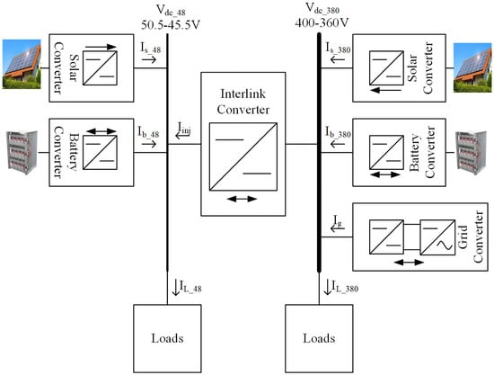
Figure 1.
Dual DC Bus Nanogrid.
In terms of research and development of the interlink converter, one should select a suitable power topology with rated voltages of 48 V:380 V, a modulation/control scheme, as well as define an appropriate control strategy (V-I curve) for the interlink converter to operate with DC bus signaling (DBS). The latter should be done in a way as to not interfere with the conventional approach of managing power and energy in a single-bus DC nanogrid. It should be noted that although 48 V and 380 V, as stated before, are ELV and LV, they would be called LV side and HV side, respectively, in this work.
This paper introduces a nanogrid system with dual DC buses, namely a low voltage (48 V) bus and a high voltage (380 V) bus, which are interconnected through an interlink converter responsible for managing the power flow between them. The buses at the booth are equipped with various resources such as renewable energy sources (RESs), storage systems, and load. Furthermore, the paper proposes V-I curves for the power interfaces that manage the power sharing in decentralized control of the dual DC bus nanogrid through DC bus signaling and droop control. The present paper introduces a control strategy for the interlink converter to enhance the power balance of the two buses. Additionally, the authors analyze the small signal model of the dual active bridge in its capacity as an interlink converter. The authors validated the proposed dual DC bus nanogrid through simulation results utilizing MATLAB/Simulink.
2. Power Control and Current Sharing in a Single DC Bus Nanogrid
A conventional single-bus DC nanogrid can be decentralized with a hierarchical structure with DC bus signaling (DBS) and droop control used at the primary level [7,13,28,29,30,31,32]. In addition, adaptive droop control could be used to improve the power sharing for parallel DC–DC converters [33]. This work does not consider the secondary and tertiary levels, which require a communication means for energy management. Thus, with fixed parameters for the primary control level, the DC bus voltage will vary in a small range around the rated voltage, as defined by the V-I curves of the DERs. DBS uses the DC bus voltage as the communication link to coordinate the operation of DERs in a decentralized way. With droop control, the current (power) injected by each DER in the DC nanogrid depends on its threshold voltage (VNL), where the injected current is zero, and its droop slope/factor (Rd) is shown in (1). The latter determines how the injected current varies as a function of grid voltage variations.
where;
Figure 2 shows the V-I curves of the standard components found in a DC nanogrid with a proposed set of parameters [7,13,30]. The DC–AC grid converter is discussed first. When the DC bus voltage is between 390 V and 370 V, the converter operates in droop mode with a droop constant (slope) Rdg. Otherwise, it operates in current-limiting mode, with the DC–AC converter absorbing rated current for VDC > 390 V and supplying for VDC < 370 V. Its threshold, or no-load, voltage is the rated voltage of the DC bus: 380 V. That is to say that at this voltage, the current and power flowing through the converter is zero. The values of the threshold voltage and the DC bus voltage determine the power-flow direction. When the DC bus voltage is higher than 380 V but lower than 390 V, power flows from the DC nanogrid into the AC utility grid (Ig < 0 A). Conversely, for DC bus voltage lower than 380 V but higher than 370 V, power flows to the DC nanogrid from the AC utility grid (Ig > 0 A). The threshold voltage is the main control parameter of this DC–AC converter, which the secondary control level can adjust.
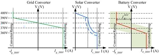
Figure 2.
V −I curves of the high voltage DC bus DERs: Grid Converter, Solar Converter, and Battery Converter.
In the case of the RESs, such as the solar converter, the V. vs. I curve usually presents three regions: droop, constant power, and constant current, as shown in Figure 2. It operates with droop constant Rds for a DC bus voltage between 400 V (threshold voltage) and 390 V when the converter starts to operate in the maximum power point tracking (MPPT) mode with the maximum available power injection. In the concept of DC bus signaling, a higher threshold voltage for the solar converter than the grid converter gives the RESs a higher priority to feed the DC nanogrid demand/load when operating in parallel. The following section will discuss the actual power flow between the solar converter, grid converter, battery, and variable load. For DC bus voltages between 390 V and 360 V, the converter operates in the maximum power point tracking (MPPT) mode injecting virtually constant power for constant solar irradiance (W/m2). The dashed line in this region shows that the solar converter is reprogrammed to operate in MPPT mode, injecting the maximum available power when the solar irradiance decreases from the rated value or the PV panel temperature increases [7]. When the DC bus voltage drops below 360 V, the solar converter operates at the current-limiting mode.
The electrical storage units operate in droop mode, with droop constant Rdb when the DC bus voltage is between 380 V and 360 V. Otherwise, it operates in the current-limiting mode, absorbing rated current for VDC > 380 V and supplying for VDC < 360 V. The storage system usually has the third priority, after the RESs and the utility grid, to feed the load. It has a threshold voltage of 370 V, lower than the other system interfaces. This prevents the electrical storage system from discharging through the utility grid. On the other hand, the electrical storage system is discharged at DC bus voltages less than 370 V.
Concerning power-flow control and energy management in the DC nanogrid, the actual value of the threshold voltage of the power interfaces can be adjusted based on the instantaneous and historical price of energy that could be drawn from or supplied to the utility grid. Long- and/or short-term histories of the local renewable energy generation and the nanogrid load profiles play a role in reprograming the threshold voltage. In addition, the history of the storage units’ state of charge (SoC) should be considered. To achieve optimal threshold voltage preprogramming, an optimal energy utilization algorithm is used [7]. To implement this algorithm, historical data about the system is needed. The maximum charging and discharging current are based on the battery manufacturer and power-converter ratings. Sometimes, when the SoC drops below 20%, the control will stop the discharging operation mode. On the other hand, the battery will not be charged when it has a SoC greater than 90% [34]. The current limits could be a function of the state of charge (SoC) [7,35,36,37]. This produces the shaded area in the V-I curve, as shown in Figure 2.
Neglecting the voltage drops between the DER interfaces and the equivalent system load, the DC bus voltage (VDC) of a nanogrid operating with DBS and multiple DERs can be determined from the:
where IDC_i are computed according to the V-I curves of the n DERs, with the value of VDC, one can then calculate the individual contributions of the DERs from their V-I curves.
3. Power Control of the Interlink Converter
As a conventional single-bus DC nanogrid, the dual DC bus nanogrid could be decentralized with a hierarchical structure based on droop control and DC bus signaling [7,28,29]. In principle, the V-I curves and parameters of the DERs in the LV DC and HV DC buses could be the same as in the case of a single-bus DC nanogrid. For instance, it is assumed that the values of threshold voltages, droop slopes, and current limits for the DERs in the LV bus are proportional to those of the HV side, shown in Figure 2. With the addition of the interlink converter, an opportunity for optimizing the operation of both buses arises in terms of voltage regulation and management of power flow and energy management. For that, a suitable strategy for controlling the power flow of the interlink converter is needed. Ideally, it should be based on DBS, considering the voltages of both DC buses, which reflect the power availability in those buses. Considering that the batteries are the weak link in the system since they are not supposed to be over- or undercharged, the control law of the interlink converter must not place unnecessary stress on them. In addition, in terms of managing the system to operate efficiently, having the battery of one bus charge, and the battery of the other should be avoided.
Two control strategies for the interlink converter in a dual DC bus nanogrid, average droop control, and constant-voltage ratio, were presented in [38]. The first determines the power flow between the two buses based on the average value obtained from droop curves of the LV and HV sides. On the other hand, the second employs a PI controller to keep the per-unit voltage ratio constant between the two buses without a V-I curve. Those control strategies can be used for a dual DC bus nanogrid with similar RESs and storage unit participations, but they should not be used when the dual DC nanogrid is connected with the AC utility grid.
This paper presents an alternative approach to control the interlink converter, which is to use, in principle, the same V-I curve of the grid converter of the HV bus. Recall that this is controlled based only on the HV DC bus’s voltage, neglecting the AC bus’s voltage. This is reasonable since the latter is assumed to be much stronger, with more power availability, than the former and can supply/absorb the matching power for/from the HV DC bus. By making the control of the interlink converter based on the voltage of the LV bus only, one does not compromise the ability of the HV bus to operate without stressing its storage units since the grid converter is there to provide/absorb the required matching power.
Therefore, one can use the V-I curves shown in Figure 3 for the interfaces of the LV DC bus. Note that the voltage levels, in terms of pu, are comparable to those employed in the HV DC bus. The voltage range in normal operating conditions varies by about 5% above and below the rated voltage (48 V).
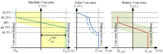
Figure 3.
Low voltage 48 V DC bus V-I characteristics: Interlink Converter, Solar Converter, and Battery Converter.
Based on the V-I curves in Figure 3, one can say that the LV DC bus battery will not be discharged into the HV DC bus. The LV DC bus is discharged with DC bus voltages less than 46.75 V, and, at this DC bus voltage, power should flow from the HV DC bus to the LV DC bus, according to the interlink converter V-I characteristic. To avoid power flowing from the LV DC bus to the HV DC bus at light load conditions or when the utility grid cannot absorb the excess power, the interlink converter (current) limits should be reprogrammed. They are changed based on the HV DC bus voltage, as shown in Figure 4. In addition, Figure 4 shows that the interlink converter (current) limits are reprogrammed to prevent the HV DC bus battery from discharging into the LV DC bus.
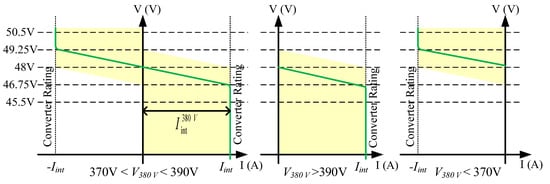
Figure 4.
Interlink converter current limit reprogrammed based on the HV DC bus: 370 V < VHV < 390 V, VHV > 390 V, and VHV < 370 V.
4. Interlink Converter Modeling and Control Design in Dual DC Buses Nanogrid
Figure 5 shows the schematic of a full-bridge isolated bidirectional DC–DC converter called a dual active bridge (DAB) [39,40,41]. It can provide a high voltage gain using a high-frequency transformer with a small volume and weight. Moreover, the DAB provides galvanic isolation between the two DC buses and there is no need for the circuit breakers to isolate the buses at fault conditions in one of them [42]. There, VLV and VHV are the LV and HV DC bus voltages, respectively, S1 −S4 and Q1 −Q4 are the controllable switches, n is the transformer’s turn ratio, and L is the equivalent leakage inductance of the transformer.
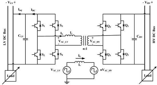
Figure 5.
Full-bridge isolated DC–DC converter (DAB).
The DAB DC–DC converter is controlled with phase-shift control in this work. There are many types of phase-shift control in the literature [39,40,41,43]. However, the most common one (and suitable for this application) is the single-phase-shift (SPS) control shown in Figure 6 [31]. All the switches are gated in this control scheme with a 50% duty cycle. S1 and S4 are switched as a pair, complementarily to S2 and S3 in the first full bridge. Likewise, Q1 and Q4 are switched complementarily to Q2 and Q3 in the second HV side bridge. That generates square waveforms, VAC_HV and VAC_LV, at the transformer’s terminals. As in traditional AC power-transmission systems, the inductor current’s direction and magnitude can be adjusted by changing the phase shift between the two square waves. This allows the control of the direction and magnitude of the power flow [43,44,45]. This is achieved with a single control parameter, the phase-shift ratio (d), for an actual phase shift (πd) between VAC_HV and VAC_LV.
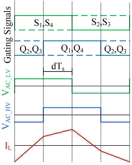
Figure 6.
SPS Control waveforms.
The power injected into the LV side of the DC–DC converter in Figure 5 can be expressed as follows for SPS control [39,46]:
where fs is the switching frequency and VAC_HV and VAC_LV are the transformer’s high and low side voltages. By ignoring the voltage loss of the power switch, VAC_HV could equal VHV and −VHV, while VAC_LV could equal VLV and −VLV. From Equation (4), the power has a maximum value when the phase-shift ratio (d) is 0.5. Figure 7 shows the power injected by the 48 V bus vs. the phase −shift ratio (d). Power flows from the HV side to the LV side at positive phase shifts (0 < πd < π) and from the LV side to the HV side at negative phase shifts (−π < πd < 0).
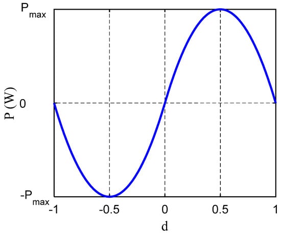
Figure 7.
Power injected by the LV bus vs. phase −shift ratio.
Then, the average value of the current at the LV side (IDC) is [46]:
Therefore, the large signal model for the DAB can be obtained by replacing the two full bridges and the HV voltage with a current source of magnitude given in (5) and the large signal equivalent circuit is shown in Figure 8 [46]. Moreover, the LV DC bus could be modeled using Thevenin’s equivalent circuit with a threshold voltage VNL_LV and a droop resistance RdLV. Then, the DAB in the dual DC buses nanogrid could be modeled with respect to the LV side in the dual DC nanogrid, as shown in Figure 9.
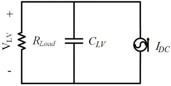
Figure 8.
Equivalent circuit of DAB feeding a resistive load.
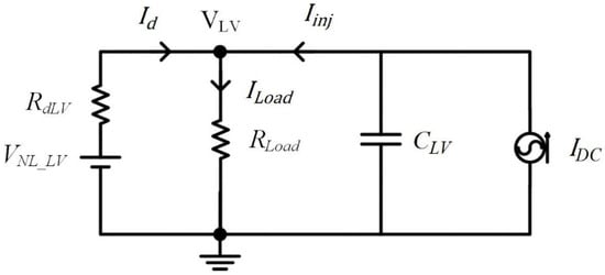
Figure 9.
Equivalent circuit of DAB in dual DC buses nanogrid with respect to LV side.
For the study of the dynamic response of the DAB, the expression for the average value of the current injected in the LV DC bus should be linearized around an operating point, leading to a small signal model as in (6) [46]. However, the injected current ῖinj(s) as a function of the phase-shift ratio is needed to control the DAB based on the proposed V-I curve. The small signal model for the DAB DC–DC converter with SPS reflected the LV side in the DC nanogrid, assuming that the equivalent threshold voltage of the LV bus (VNL_LV) is constant, is shown in Figure 10.
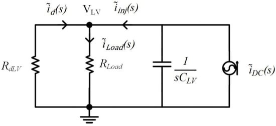
Figure 10.
Small signal model of DAB in dual DC buses nanogrid with respect to LV side.
Then, one gets the following expression for the current injected by the interlink converter into the LV DC bus (ῖinj(s)) as a function of variations in the phase-shift ratio ().
The transfer function of the DAB for the design of the current controller becomes.
5. Case Study
As a case study in this work, a DAB, as in Figure 5, is used as an interlink converter with the following parameters: transformer-turns ratio n = 0.25, leakage inductance L = 300 µH, switching frequency fs = 20 kHz, and HV and LV capacitors CHV = CLV = 1500 µF. The LV DC bus is modeled by a Thevenin equivalent with the DC voltage VNL_LV = 49.25 V and a droop constant RdLV = 0.289 Ω. In addition, the HV DC bus is modeled by Thevenin’s with the DC voltage VNL_HV = 390 V and a droop constant RdHV = 0.289 Ω. Table 1 summarises the case-study parameters.

Table 1.
The case-study parameters.
For a load resistance of 10 Ω, the transfer function of the plant becomes:
Then, a PI type-II compensator (10) is designed for a cut-off frequency of [31] and a phase margin PM = 80°, as illustrated in the following steps:
Step 1: From the Bode plot of the plant, obtain and .
Step 2: Step 4: Calculate the and :
Step 3: Calculate the controller parameters:
- Boost:
- K factor:
- Zeros and Poles:
- Gain:
The compensator parameters are τ = 991 µs, TP = 443 µs, and KPI = 0.15. Figure 11 shows the Bode plot for the plant (G), the controller (C), and the loop transfer function (CG).
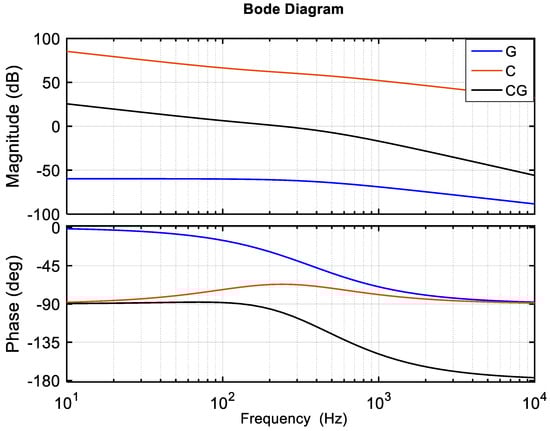
Figure 11.
The Bode plot of the model (G), the controller (C), and the combination (CG).
For the current or power sharing, the interlink converter is controlled with the V-I curve in Figure 3, with threshold voltage VNL_int = 48 V and Rdint = 0.289 Ω. The injected current (Iinj) from DAB is given by the droop equation (1) in the droop mode or constant at 4.325 A in the current-limiting mode. The control block diagram is shown in Figure 12. The phase-shift PWM control used in this work is realized, as shown in Figure 13. The HV side triangular waveform was shifted by 0.25 duty cycle (π/2) to allow negative delay using a time delay block. The fixed duty cycle is used to be 0.499 instead of 0.5 to implement a small dead time for the switches.
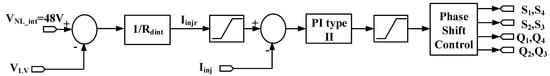
Figure 12.
Control block diagram.
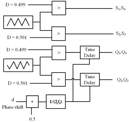
Figure 13.
Phase-shift PWM block.
6. Simulation Results
Two simulation results were obtained considering the dual DC bus nanogrid discussed in this paper. The first is to test the DAB as an interlink converter. That can be done by verifying the SPS modulation waveforms described in Figure 6. Then, test the proposed model of the DAB in the DC nanogrid. Finally, test the ability of the interlink converter to direct the power between the two DC buses, as described in Figure 4. The second test is regarding the full dual DC bus nanogrid in Figure 1 and controlling the power and the current sharing with the V-I curve presented in Figure 2 and Figure 3.
6.1. Simulation Results of DAB as Interlink Converter
MATLAB/Simulink is used to simulate the DAB in Figure 5 with the case-study parameter and control loop presented in Section 4. The first is an open loop test to verify the SPS modulation waveforms of the DAB described in Figure 6. Figure 14 shows the gating signals of the LV and HV sides of DAB, the AC voltage at the LV and HV sides of the transformer, and the transformer leakage inductor current at d = −0.25. The results show that the phase-shift PWM block in Figure 13 works as expected to perform the required modulation for the DAB.
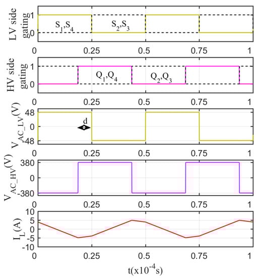
Figure 14.
Simulation result of SPS modulation waveforms.
The second test is to verify the performance of the control loop of the current injected into the LV bus. Again, the voltages of the LV and HV sides are set at 48 V and 380 V, respectively. The reference current is initially at −1.5 A, then changed in a step to 1.5 A. As shown in Figure 15, the injected current Iinj follows the reference signal very well, reaching the steady state at 0.007 s with zero error. The negative injected current Iinj sign means that the power flow is from the LV to the HV side, achieved with a negative phase shift. Conversely, a positive injected current Iinj means the power flow from the HV side to the LV side, requiring a positive phase shift.
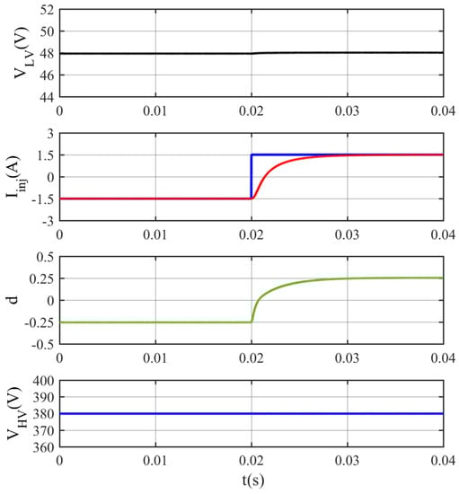
Figure 15.
Simulation results for a step change in the injected reference current.
The last test investigates the impact of load variations in both DC buses and the power flow controlled by the interlink converter, according to the proposed droop control scheme, on the LV and HV buses’ voltages. Three cases are considered: first with 370 V < VHV < 390 V, then with VHV < 370 V, and finally with VHV > 390 V. As discussed before, the interlink converter is droop-controlled based on the magnitude of the voltage at the LV bus, but for low and high at the HV bus, it should be reprogrammed to prevent worsening the problem of excess surplus or shortage of power in that bus.
Threshold voltages and droop resistances modeled the LV DC bus and HV DC bus. For the LV DC bus, VNL_LV = 49.25 V and RdLV = 0.289 Ω, while for the HV DC bus, VNL_HV = 390 V and RdHV = 0.289 Ω. In this case, the LV DC bus voltage can be calculated by (11) through the droop Equation (1) with an equivalent threshold voltage of VNL_eq = 48.625 V, obtained considering the threshold voltages of the LV DC bus and interlink converter, and a droop constant Rdeq = 0.1445 Ω, the parallel combination of RdLV and Rdint. For a given current injected by the DAB into the LV side, the current drawn from the HV side will be much smaller due to the transformer’s turn ratio. The HV DC bus voltage can be calculated by (11) through the droop Equation (1) with a threshold of VNL_HV and a droop constant of RdHV.
The simulation results are shown in Figure 16. Initially, both DC buses are connected to 80 Ω loads, presenting voltages VLV = 48.54 V and VHV = 388.6 V. The value of the current injected into the LV bus (Iinj) is −1.87 A, determined by the V-I droop characteristic of the interlink converter. With VLV = 48.54 V higher than VNL_int = 48 V, power is shown to be drawn from the LV bus and sent to the HV bus. At t = 0.02 s, an additional 40 Ω is connected to the LV side, resulting in a decrease in the voltage at that bus, VLV = 48.36 V, and in the current, the interlink converter draws power from the LV bus, Iinj = −1.26 A. The change, a reduction, in VHV is minimal due to the small value of the LV side current reflected to the HV side current, and transformer turns ratio. At t = 0.04 s, an additional 40 Ω is connected to the HV side and, since the reference value for the current of the interlink is a function of the LV DC bus only, the injected current does not change; the HV DC bus voltage becomes VHV = 385.8 V, lower than before. At t = 0.06 s, an additional 20 Ω is connected to the LV side, reducing the voltage in the LV bus to VLV = 48 V, which makes Iinj ≈ 0 A. At t = 0.08 s, an additional 20 Ω is connected to the HV side; again, it does not affect the power sharing and the HV DC bus voltage drops to VHV = 380.4 V. At t = 0.1 s, an additional 40 Ω is connected to the LV side, reducing the voltage at this DC bus below 48 V VLV = 47.85 V, and the power starts to flow from the HV DC bus to the LV DC bus with injected current: Iinj = 0.52 A. At t = 0.12 s, an additional 40 Ω is connected to the HV side and, again, it does not affect the power sharing, and the HV DC bus voltage drops to VHV = 377.7 V. At t = 0.14 s, an additional 20 Ω is connected to the LV side; therefore, the injected current increases Iinj = 1.73 A and this means more power flow from the HV side to the LV side with more drop in the LV DC bus VLV = 47.5 V. Finally, at t = 0.16 s, an additional 20 Ω is connected to the HV side and it does not affect the power sharing, and the HV DC bus voltage drops to VHV = 372.5 V. The results show that the power injected by the interlink converter does not depend on the HV voltage side, as the V-I curve is a function of the LV side. In addition, the interlink converter successfully directs the power between the LV and the HV sides based on the proposed V-I curves.
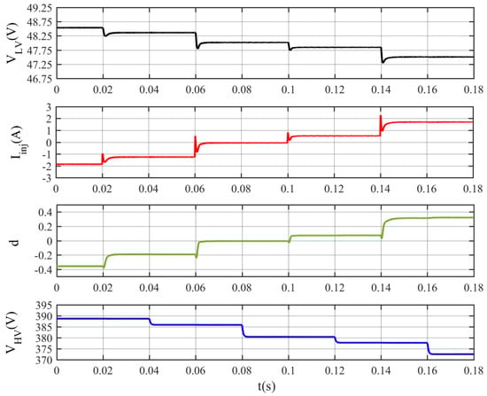
Figure 16.
Simulation results considering that 370 V < VHV < 390 V throughout the simulation time.
Figure 17 shows simulation results for a case with VNL_HV = 395 V, where the voltage at the HV bus is higher than 390 V, from t = 0 s to 0.6 s. In such a case, the proposed control law for the interlink converter should prevent any power flow to the HV bus, which already has a surplus of power. Initially, both DC buses are connected to 80 Ω loads, presenting voltages VLV = 49.32 V and VHV = 393.6 V. At t = 0.02 s, an additional 40 Ω load is connected to the HV DC bus, VHV decreases to 390.8 V, and there is no power flow from the LV to the HV DC bus. At t = 0.04 s, an additional 40 Ω load is connected to the LV DC bus, VLV = 48.72 V, still higher than 48 V, and there is no power flow from the LV to the HV DC bus because of the voltage at the HV bus. At t = 0.06 s, an additional 40 Ω load is connected to the HV DC bus, VHV drops to 385.26 V, below 390 V, and power starts to flow from the LV to the HV DC bus. Due to that, VLV drops to 48.36 V with Iinj = −1.25 A as the V-I curve in Figure 4. At t = 0.08 s, an additional 40 Ω load is connected to the LV DC bus, VLV ≈ 48 V, which makes Iinj ≈ 0 A. In this case, there is no power flow from the LV DC to the HV DC but now it is due to VLV ≈ 48 V= VNL_int. After that, power flow from the HV to the LV DC bus increases at t = 0.12 s and t = 0.16 s, when loads are added to the LV bus, but not at t = 0.14 s, when there is a load increase in the HV DC bus. The results show that the proposed interlink V-I curve could prevent power flow from the LV to the HV side when the HV bus has a voltage higher than 390 V, which means that the HV DC bus cannot supply power to the grid for some reasons.
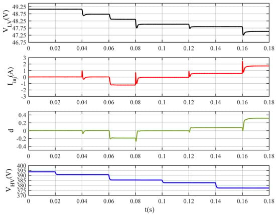
Figure 17.
Simulation results for the case where VHV > 390 V for a specific time interval.
Figure 18 shows simulation results for a case with VNL_HV = 380 V, where the HV DC bus is lower than 370 V, from t = 0.1 s to 0.18 s. In such a case, the proposed control logic of the interlink converter prevents the power flow from the HV DC bus to the LV DC bus, achieved by reprogramming the current limit as in Figure 4, Iinj = 0. To prevent the HV DC bus batteries from discharging through the LV DC bus, initially, both DC buses are connected to 80 Ω loads, presenting voltages VLV = 48.54 V and VHV = 378.63 V with Iinj = −1.87 A, meaning that power flows from the LV to the HV side. At t = 0.02 s, an additional 40 Ω load is connected to the HV DC bus and VHV decreases to 375.9 V without changes in the current of the interlink converter. At t = 0.04 s, an additional 40 Ω load is connected to the LV DC bus, and VLV decreases to 48.36 V, indicating a reduction of the power surplus on the LV side, which makes Iinj reduce to −1.26 A. At t = 0.06 s, an additional 40 Ω load is connected to the HV DC bus and VHV drops to 370.63 V. At t = 0.08 s, an additional 40 Ω load is connected to the LV DC bus, VLV ≈ 48 V, which makes Iinj ≈ 0 A. In this case, there is no power flow from the LV DC to the HV DC since VLV ≈ 48 V = VNL_int. At t = 0.1 s, an additional 40 Ω load is connected to the HV DC bus and VHV drops to 368.05 V, below 370 V, and the interlink should prevent the power flow from the HV DC bus to the LV DC bus as described in Figure 4. Therefore, at t = 0.12 s, when an additional 40 Ω is connected to LV DC, Iinj = 0, indicating that power does not flow from the HV DC bus to the LV DC bus, even though VLV = 47.7 V, < VNL_int = 48 V, as discussed in Figure 4. After that, power flow from the HV to the LV DC bus is still prevented at t = 0.14 s and t = 0.16 s when loads are added to the HV bus and LV bus, respectively. The results show that the proposed interlink V-I curve could prevent power flow from the HV to the LV side when the HV side has a voltage less than 370 V, which prevents the HV side batteries from discharging into the LV side.
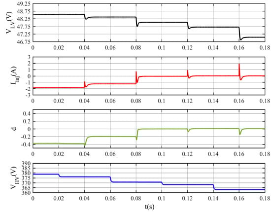
Figure 18.
Simulation results for the case where VHV < 370 V for a specific time interval.
6.2. Simulation Results of Dual DC Buses Nanogrid
MATLAB/Simulink is used to simulate the dual DC buses nanogrid in Figure 19 under different operation conditions. A class C DC–DC converter, as in Figure 19, is used as the main power electronics interface of the DERs: solar panels and batteries. A class C DC–DC converter is also used along with a DC–AC converter as the two-stage AC grid interface.
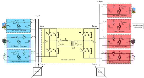
Figure 19.
Dual DC buses nanogrid power electronics interfaces.
Regarding the power and the current sharing, the V-I in Figure 2 and Figure 3 were used. For the HV DC bus DERs, a 5 kW PV panel and battery were considered with a droop constant RdS_380 = RdB_380 = 0.763 Ω, and a 10 kW grid connection was considered with a droop constant RdG = 0.3815 Ω. They resulted in 14.2 A, 13.11 A, and 26.22 A as current limits for the solar, battery, and grid converters. For the LV DC bus DERs, a 2 kW PV panel, battery, and interlink were considered with a droop constant RdS_48 = RdB_48= Rdint = 0.0289 Ω. They resulted in a 44 A current limit for the solar converter and a 43.25 A current limit for the battery and interlink converters. The supercapacitors (SC) were controlled to support the dynamics of the battery’s current by splitting the storage inductor current into low frequencies for the battery and high frequencies for the SC using a low-pass filter (LPF) with a 30 Hz cut-off frequency.
The same current control loop parameters can be used for all DERs at the same DC bus. A PI type-III controller was designed for the same equivalent plant with a transfer function shown in (12) [47,48]. They were designed for a crossover frequency of fx = 2 kHz (10% of the switching frequency) and a phase margin of PM = 80° for both DC buses. For the LV DC bus converters, the following plant parameters were used: Vout = VDC = 48 V, IDC = 41.67 A, R = 1.152 Ω, L = 300 µH, C = 1500 µF, and D = 0.46 for VPV = VB = VSC = 29 V. R was selected as the maximum load that could be supplied by the RES alone. Finally, the PI controller parameters are computed as KPI = 0.0117, τ = 175 µs, and TP = 36 µs. For the HV DC bus converters, the following plant parameters were used: Vout = VDC = 380 V, IDC = 13.16 A, R = 27.94 Ω, L = 3000 µH, C = 1500 µF, and D = 0.39 for VPV = VBat = VSC = 232 V. R was selected as the maximum load that could be supplied by the RES alone. Finally, the PI controller parameters are computed as KPI = 0.0015, τ = 171 µs, and TP = 37 µs. The interlink converter with the following parameters: transformer turns ratio n = 0.25, leakage inductance L=10.7 µH, switching frequency fs = 20 kHz, and HV and LV capacitors CHV = CLV = 1500 µF. Then, a PI type-III compensator is designed for a cut-off frequency of 240 Hz [31] and a phase margin PM = 80°. Therefore, the compensator parameters can be calculated as τ = 1.4 ms, TP = 318 µs, and KPI = 0.049 at a load resistance of 1.15 Ω.
The first test of the dual DC buses nanogrid is with a grid connection, and the batteries are not fully charged. The indication of the load variations in the system with the respective times and the numerical values of the voltage and current waveforms shown in Figure 20 and Figure 21 are summarized in Table 2 and Table 3 for the HV DC bus and the LV DC bus, respectively. The figures demonstrate that while the grid, the interlink, and the battery converters operate with droop control, the solar converters operate at the MPPT. The grid converter supports the HV bus and indirectly the LV bus through the interlink converter with Iint = 2 A when a 305 Ω load is initially attached to the HV bus and 40 Ω to the LV bus. The LV bus load increased to 7 Ω at t = 0.1 s and additional support came from the HV bus at Iint = 4.8 A, which raised the grid current to 5.3 A. At t = 0.2, the HV DC bus increased to 63.4 Ω; the grid current changed to 5.2 A to support the HV bus, while the interlink converter current remained constant because it depended on the LV bus. Figure 20 shows that the grid current varied when the HV bus load or LV bus changed, while Figure 21 shows that the interlink converter current changed when the LV bus load changed. Based on these results, the nanogrid operates according to the V-I curves presented in Figure 2 and Figure 3 for the HV DC and LV DC buses, respectively. The RESs operate at maximum power. At the HV DC bus, the battery and the grid converter operate with droop control, the battery is in charging mode, and the grid supports the nanogrid by supplying power. At the LV DC bus, the battery and the interlink converter operate with droop control, the battery is in charging mode, and the interlink supports the LV DC bus. In addition, Figure 20 and Figure 21 show that the PI type III controller successfully controls the dynamic response of the converters where the currents reach the steady state in almost 10 ms. However, the batteries’ currents are much slower than other resources due to hybrid energy storage between the supercapacitors and the batteries, which is more efficient for the batteries.
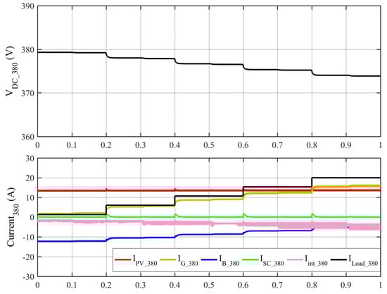
Figure 20.
Simulation results of the dual DC buses nanogrid with grid connection—the HV DC bus waveforms.
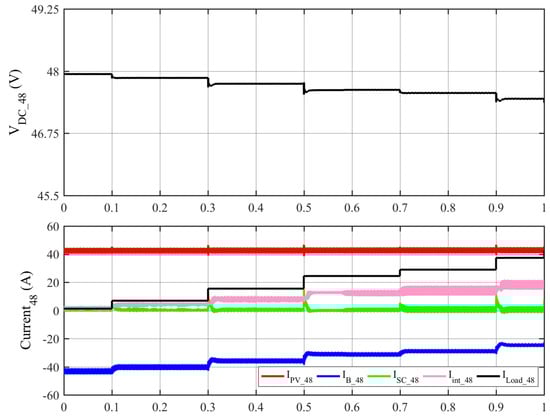
Figure 21.
Simulation results of the dual DC buses nanogrid with grid connection—the LV DC bus waveforms.
Table 2.
Numerical results of the HV DC bus from Figure 20.
Table 3.
Numerical results of the LV DC bus from Figure 21.
The second test of the dual DC buses nanogrid is without a grid connection, and the batteries are not fully charged. The indication of the load variations in the system with the respective times and the numerical values of the voltage and current waveforms shown in Figure 22 and Figure 23 are summarized in Table 4 and Table 5 for the HV DC bus and the LV DC bus, respectively. Based on these results, the nanogrid operates with the V-I presented in Figure 2 and Figure 3 for HV DC and LV DC buses, respectively. By comparing the cases above, one can say that the grid connection gives the DC nanogrid more power availability; missing this support leads to a higher voltage drop in the DC buses, especially at the HV DC bus. Moreover, the battery started to discharge at t = 0.6 s while in the charging mode with the grid connection.
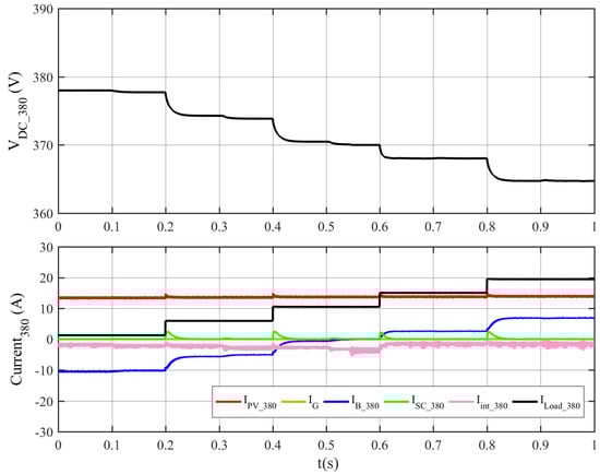
Figure 22.
Simulation results of the dual DC buses nanogrid without grid connection—the HV DC bus waveforms.
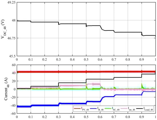
Figure 23.
Simulation results of the dual DC buses nanogrid without grid connection—the LV DC bus waveforms.
Table 4.
Numerical results of the HV DC bus from Figure 22.
Table 5.
Numerical results of the LV DC bus from Figure 23.
Regarding the LV DC bus, the effect of missing the grid connection is less once the HV DC bus is higher than 370 V due to the power and current sharing V-I being based on the LV DC bus. Therefore, there is no change in the LV DC bus before t = 0.5 s according to Table 5 compared to Table 3. At t = 0.6 s, the HV DC load was increased to 24.5 Ω, and the HV DC bus dropped below 370 V; the HV battery operates in discharging mode and the interlink converter prevents the power flow from the HV DC to the LV DC bus (Iint = 0), so the HV DC bus battery will not discharge through the LV DC bus. After t = 0.6 s, the LV DC bus misses the support from the HV DC bus. Therefore, the voltage drops in the LV DC bus in Table 5 increase compared with the case with grid connection in Table 3 at the same load level. The RESs operate at maximum power at all periods. Moreover, the interlink converter prevents the LV and HV side batteries from discharging to charge each other. In addition, Figure 22 and Figure 23 show that the PI type III controller successfully controls the dynamic response of the converters where the currents reach the steady state in almost 10 ms. However, the batteries’ currents are much slower than other resources due to hybrid energy storage between the supercapacitors and the batteries, which is more efficient for the batteries.
7. Conclusions
This research presents a nanogrid system with a dual DC bus configuration, including a bidirectional interlink converter capable of directing the power flow between the two buses. The high voltage (HV) bus provides power to high-power appliances, while the low voltage (LV) bus supplies energy to low-power loads. Nanogrid reliability was enhanced by integrating distributed energy resources on the two buses. Furthermore, a control methodology utilizing DC bus signaling (DBS) is suggested, which facilitates the assessment of the impact on the DC buses in the presence of other DERs controlled by DBS. It is commonly observed that the HV bus is more robust than the LV bus. As a result, the voltage at the LV side determines the power flow between DC buses. The above statement is equivalent to the V-I curve of an AC grid converter operating within a single DC bus nanogrid. This implies that the power delivered by the interlink converter is independent of the voltage on the high voltage side since the low voltage side determines the V-I curve.
Furthermore, utilizing the suggested V-I curve, the interlink converter effectively facilitates power transfer between the low voltage (LV) and high voltage (HV) sides. If the high voltage (HV) bus exhibits a significant excess or lack of power, identified by its bus voltage (VHV), the interlink converter is prevented from worsening these circumstances. One potential solution involves implementing a mechanism that prevents power transfer from the low voltage (LV) to the high voltage (HV) side in instances where the HV bus voltage exceeds 390 V. This would effectively prevent the HV DC bus from supplying power to the grid under certain circumstances. Additionally, preventing power flow from the HV to the LV side would be necessary in cases where the HV side voltage falls below 370 V, as this would prevent the discharge of HV side batteries into the LV side. The characteristic above is essential to dual DC bus nanogrids that function continuously or intermittently disconnected from the AC utility grid. In addition, a topology that is considered appropriate for the interlink power converter is chosen. This topology is bidirectional, has high gain, and is equipped with galvanic isolation. It is commonly referred to as the dual active bridge (DAB). A dynamic model has been proposed for the interlink converter. This converter operates using a single phase-shift modulation scheme and behaves within a droop-controlled environment. A closed-loop controller has been developed to regulate the current injected into the LV DC bus based on the voltage of the bus. The performance of the droop-controlled interlink converter in a dual DC bus nanogrid is examined via MATLAB/Simulink simulations. Per the proposed approach, the interlink converter effectively manages power sharing between the HV and LV buses.
Author Contributions
Conceptualization, A.M.A.M.; Methodology, A.M.A.M. and L.A.C.L.; Validation, A.M.A.M.; Formal analysis, A.M.A.M.; Investigation, A.M.A.M.; Writing—review & editing, A.M.A.M. and A.A.-Q.; Visualization, L.A.C.L.; Supervision, L.A.C.L. All authors have read and agreed to the published version of the manuscript.
Funding
This research was funded by the The University of Jordan and Natural Sciences and Engineering Research Council (NSERC) of Canada.
Data Availability Statement
Data are available upon request.
Acknowledgments
The authors appreciate the financial support provided by The University of Jordan, through the Deanship of Scientific Research, and of the Natural Sciences and Engineering Research Council (NSERC) of Canada.
Conflicts of Interest
The authors declare no conflict of interest.
Abbreviations
| RES | Renewable Energy Source |
| ICT | Information and Communication Technology |
| DER | Distributed Energy Resources |
| NZEH | Net-Zero Energy Homes |
| ELV | Extra Low Voltage |
| LV | Low Voltage |
| HV | High Voltage |
| DBS | DC Bus Signaling |
| MPPT | Maximum Power Point Tracking |
| SoC | State of Charge |
| DAB | Dual Active Bridge |
| SPS | Single-Phase Shift |
| d | Phase-Shift Ratio |
| PWM | Pulse Width Modulation |
References
- Alepuz, S.; Busquets-Monge, S.; Bordonau, J.; Gago, J.; Gonzalez, D.; Balcells, J. Interfacing Renewable Energy Sources to the Utility Grid Using a Three-Level Inverter. IEEE Trans. Ind. Electron. 2006, 53, 1504–1511. [Google Scholar] [CrossRef]
- Gungor, V.C.; Sahin, D.; Kocak, T.; Ergut, S.; Buccella, C.; Cecati, C.; Hancke, G.P. Smart Grid Technologies: Communication Technologies and Standards. IEEE Trans. Ind. Inform. 2011, 7, 529–539. [Google Scholar] [CrossRef]
- Bryan, J.; Duke, R.; Round, S. Distributed generation-nanogrid transmission and control options. In Proceedings of the International Power Engineering Conference, Singapore, 27–29 November 2003; pp. 341–346. [Google Scholar]
- Leonori, S.; Rizzoni, G.; Mascioli, F.M.F.; Rizzi, A. Intelligent energy flow management of a nanogrid fast charging station equipped with second life batteries. Int. J. Electr. Power Energy Syst. 2020, 127, 106602. [Google Scholar] [CrossRef]
- Rubio, C.; Siddiqui, A. Shape of the microgrid. In Proceedings of the 2001 IEEE Power Engineering Society Winter Meeting, Columbus, OH, USA, 28 January–1 February 2001; pp. 150–153. [Google Scholar]
- Lakhina, U.; Elamvazuthi, I.; Badruddin, N.; Jangra, A.; Truong, B.-H.; Guerrero, J.M. A Cost-Effective Multi-Verse Optimization Algorithm for Efficient Power Generation in a Microgrid. Sustainability 2023, 15, 6358. [Google Scholar] [CrossRef]
- Boroyevich, D.; Cvetković, I.; Dong, D.; Burgos, R.; Wang, F.; Lee, F. Future electronic power distribution systems a contemplative view. In Proceedings of the 2010 12th International Conference on Optimization of Electrical and Electronic Equipment, Brasov, Romania, 20–22 May 2010. [Google Scholar]
- Sartori, I.; Napolitano, A.; Voss, K. Net zero energy buildings: A consistent definition framework. Energy Build. 2012, 48, 220–232. [Google Scholar] [CrossRef]
- Muhsen, H.; Alkhraibat, A.; Al-Halhouli, A. Real-Time Simulation and Energy Management Attainment of Microgrids. Sustainability 2023, 15, 2696. [Google Scholar] [CrossRef]
- Al-Quraan, A.; Al-Mhairat, B.; Malkawi, A.M.A.; Radaideh, A.; Al-Masri, H.M.K. Optimal Prediction of Wind Energy Resources Based on WOA—A Case Study in Jordan. Sustainability 2023, 15, 3927. [Google Scholar] [CrossRef]
- Hammerstrom, D.J. AC Versus DC Distribution Systemsdid We Get it Right? In Proceedings of the 2007 IEEE Power Engineering Society General Meeting, Tampa, FL, USA, 24–28 June 2007; pp. 1–5. [Google Scholar]
- Silveira, J.P.C.; Neto, P.J.D.S.; Barros, T.A.d.S.; Filho, E.R. Power management of energy storage system with modified interlinking converters topology in hybrid AC/DC microgrid. Int. J. Electr. Power Energy Syst. 2021, 130, 106880. [Google Scholar] [CrossRef]
- Malkawi, A.; Lopes, L.A.C. Control of the power electronics interface of a PV source in a smart residential DC nanogrid. In Proceedings of the 2016 IEEE Canadian Conference on Electrical and Computer Engineering (CCECE), Vancouver, BC, Canada, 15–18 May 2016; pp. 1–4. [Google Scholar] [CrossRef]
- Committee ISC. IEEE Standard for Interconnecting Distributed Resources with Electric Power Systems; Institute of Electrical and Electronics Engineers: New York, NY, USA, 2003.
- Dong, D.; Thacker, T.; Burgos, R.; Boroyevich, D.; Wang, F.; Giewont, B. Control design and experimental verification of a multi-function single-phase bidirectional PWM converter for renewable energy systems. In Proceedings of the 2009 13th European Conference on Power Electronics and Applications, Barcelona, Spain, 8–10 September 2009; pp. 1–10. [Google Scholar]
- Thacker, T.; Burgos, R.; Wang, F.; Boroyevich, D. Single-phase islanding detection based on phase-locked loop stability. In Proceedings of the 2009 IEEE Energy Conversion Congress and Exposition, San Jose, CA, USA, 20–24 September 2009; pp. 3371–3377. [Google Scholar]
- Roggia, L.; Schuch, L.; Baggio, J.E.; Rech, C.; Pinheiro, J.R. Integrated Full-Bridge-Forward DC-DC Converter for a Residential Microgrid Application. IEEE Trans Power Electron 2013, 28, 1728–1740. [Google Scholar] [CrossRef]
- Tazy, A.; Samy, M.M.; Ghalib, M.A. Enhancement and Control of Reactive Power Sharing Utilizing Circulating Current in AC Microgrids. In Proceedings of the 2022 23rd International Middle East Power Systems Conference (MEPCON), Cairo, Egypt, 13–15 December 2022; pp. 1–5. [Google Scholar] [CrossRef]
- Balog, R.S.; Krein, P.T. Bus Selection in Multibus DC Microgrids. IEEE Trans. Power Electron. 2010, 26, 860–867. [Google Scholar] [CrossRef]
- Chen, J.; Chen, J.; Chen, R.; Zhang, X.; Gong, C. Decoupling control of the non-grid-connected wind power system with the droop strategy based on a DC micro-grid. In Proceedings of the 2009 World Non-Grid-Connected Wind Power and Energy Conference, Nanjing, China, 24–26 September 2009; pp. 1–6. [Google Scholar] [CrossRef]
- Blaabjerg, F.; Consoli, A.; Ferreira, J.; Vanwyk, J. Special Feature The Future of Electronic Power Processing and Conversion. IEEE Trans. Ind. Appl. 2005, 41, 3–8. [Google Scholar] [CrossRef]
- Correa, J.M.; Farret, F.A.; Simoes, M.; Ramos, D.B.; Ferrigolo, F.Z. Aspects of the integration of alternative sources of energy for application in distributed generation systems. In Proceedings of the XI Brazilian Power Electronics Conference, Natal, Brazil, 11–15 September 2011; pp. 819–824. [Google Scholar] [CrossRef]
- Biczel, P. Power Electronic Converters in DC Microgrid. In Proceedings of the 2007 Compatibility in Power Electronics, Gdansk, Poland, 29 May–1 June 2007; pp. 1–6. [Google Scholar]
- Sun, K.; Zhang, L.; Xing, Y.; Guerrero, J.M. A Distributed Control Strategy Based on DC Bus Signaling for Modular Photovoltaic Generation Systems with Battery Energy Storage. IEEE Trans. Power Electron. 2011, 26, 3032–3045. [Google Scholar] [CrossRef]
- Xu, L.; Chen, D. Control and Operation of a DC Microgrid With Variable Generation and Energy Storage. IEEE Trans. Power Deliv. 2011, 26, 2513–2522. [Google Scholar] [CrossRef]
- E-Merge Alliance. Public Overview of the EMerge Alliance Data. Telecom Center Standard Version. 2014. Available online: https://www.emergealliance.org/standards/data-telecom/ (accessed on 26 June 2023).
- E-Merge Alliance. Public Overview of the EMerge Alliance Occupied Space Standard. 2015. Available online: https://www.emergealliance.org/standards/occupied-space-2/ (accessed on 26 June 2023).
- Liu, C.; Chau, K.; Diao, C.; Zhong, J.; Zhang, X.; Gao, S.; Wu, D. A new DC micro-grid system using renewable energy and electric vehicles for smart energy delivery. In Proceedings of the 2010 IEEE Vehicle Power and Propulsion Conference, Lille, France, 1–3 September 2010; pp. 1–6. [Google Scholar] [CrossRef]
- Lago, J.; Heldwein, M.L. Operation and Control-Oriented Modeling of a Power Converter for Current Balancing and Stability Improvement of DC Active Distribution Networks. IEEE Trans. Power Electron. 2011, 26, 877–885. [Google Scholar] [CrossRef]
- Malkawi, A.; Lopes, L. A novel seamless control algorithm for a single-stage photovoltaic interface employing DC bus signaling. Int. J. Electr. Power Energy Syst. 2019, 113, 90–103. [Google Scholar] [CrossRef]
- Malkawi, A.M.A.; Lopes, L.A.C. Improved Dynamic Voltage Regulation in a Droop Controlled DC Nanogrid Employing Independently Controlled Battery and Supercapacitor Units. Appl. Sci. 2018, 8, 1525. [Google Scholar] [CrossRef]
- Malkawi, A.M.A.; Al-Quraan, A.; Lopes, L.A.C. Extending DC Bus Signaling and Droop Control for Hybrid Storage Units to Improve the Energy Management and Voltage Regulation. Inventions 2022, 7, 55. [Google Scholar] [CrossRef]
- Ghalib, M.A.; Samy, M.M. Magnification of Performance Operation for Low Voltage DC Microgrids Based on Adaptive Droop Control Technique. In Proceedings of the 2021 22nd International Middle East Power Systems Conference (MEPCON), Assiut, Egypt, 14–16 December 2021; pp. 424–429. [Google Scholar] [CrossRef]
- Guerrero, J.M.; Vasquez, J.C.; Matas, J.; de Vicuna, L.G.; Castilla, M. Hierarchical Control of Droop-Controlled AC and DC Microgrids—A General Approach Toward Standardization. IEEE Trans. Ind. Electron. 2011, 58, 158–172. [Google Scholar] [CrossRef]
- Noroozian, R.; Abedi, M.; Gharehpetian, G.; Hosseini, S. Combined operation of DC isolated distribution and PV systems for supplying unbalanced AC loads. Renew. Energy 2009, 34, 899–908. [Google Scholar] [CrossRef]
- Justo, J.J.; Mwasilu, F.; Lee, J.; Jung, J. AC-microgrids versus DC-microgrids with distributed energy resources: A review. Renew. Sustain. Energy Rev. 2013, 24, 387–405. [Google Scholar] [CrossRef]
- Kakigano, H.; Nishino, A.; Ise, T. Distribution voltage control for DC microgrid with fuzzy control and gain-scheduling control. In Proceedings of the 8th International Conference on Power Electronics–ECCE Asia, Jeju, Republic of Korea, 30 May–3 June 2011; pp. 256–263. [Google Scholar] [CrossRef]
- Chedid, R.; Rahman, S. Unit sizing and control of hybrid wind-solar power systems. IEEE Trans. Energy Convers. 1997, 12, 79–85. [Google Scholar] [CrossRef]
- Dalbon, W.; Roscia, M.; Zaninelli, D.; Leva, S. Hybrid photovoltaic system control for enhancing sustainable energy. In Proceedings of the IEEE Power Engineering Society Summer Meeting, Chicago, IL, USA, 21–25 July 2002. [Google Scholar] [CrossRef]
- Tsikalakis, A.G.; Hatziargyriou, N.D. Centralized control for optimizing microgrids operation. In Proceedings of the 2011 IEEE Power and Energy Society General Meeting, Detroit, MI, USA, 24–28 July 2011; pp. 1–8. [Google Scholar] [CrossRef]
- Bhaskara, S.N.; Chowdhury, B.H. Microgrids—A review of modeling, control, protection, simulation and future potential. In Proceedings of the 2012 IEEE Power and Energy Society General Meeting, San Diego, CA, USA, 22–26 July 2012; pp. 1–7. [Google Scholar]
- Zhang, L.; Wang, Y.; Cheng, L.; Kang, W. A Three-Parameter Adaptive Virtual DC Motor Control Strategy for a Dual Active Bridge DC–DC Converter. Electronics 2023, 12, 1412. [Google Scholar] [CrossRef]
- Zhang, W.; Lee, F.C.; Huang, P.-Y. Energy management system control and experiment for future home. In Proceedings of the 2014 IEEE Energy Conversion Congress and Exposition (ECCE), Pittsburgh, PA, USA, 14–18 September 2014; pp. 3317–3324. [Google Scholar] [CrossRef]
- Karlsson, P.; Svensson, J. DC bus voltage control for a distributed power system. IEEE Trans. Power Electron. 2003, 18, 1405–1412. [Google Scholar] [CrossRef]
- Kim, J.-W.; Choi, H.-S.; Cho, B.H. A novel droop method for converter parallel operation. IEEE Trans. Power Electron. 2002, 17, 25–32. [Google Scholar] [CrossRef]
- Kurohane, K.; Senjyu, T.; Yona, A.; Urasaki, N.; Muhando, E.B.; Funabashi, T. A high quality power supply system with DC smart grid. In Proceedings of the IEEE PES T&D 2010, New Orleans, LA, USA, 19–22 April 2010; pp. 1–6. [Google Scholar] [CrossRef]
- Kollimalla, S.K.; Mishra, M.K.; Narasamma, N.L. Design and Analysis of Novel Control Strategy for Battery and Supercapacitor Storage System. IEEE Trans Sustain. Energy 2014, 5, 1137–1144. [Google Scholar] [CrossRef]
- Kolluri, S.; Narasamma, N.L. Analysis, modeling, design and implementation of average current mode control for interleaved boost converter. In Proceedings of the 2013 IEEE 10th International Conference on Power Electronics and Drive Systems (PEDS), Kitakyushu, Japan, 22–25 April 2013; pp. 280–285. [Google Scholar] [CrossRef]
Disclaimer/Publisher’s Note: The statements, opinions and data contained in all publications are solely those of the individual author(s) and contributor(s) and not of MDPI and/or the editor(s). MDPI and/or the editor(s) disclaim responsibility for any injury to people or property resulting from any ideas, methods, instructions or products referred to in the content. |
© 2023 by the authors. Licensee MDPI, Basel, Switzerland. This article is an open access article distributed under the terms and conditions of the Creative Commons Attribution (CC BY) license (https://creativecommons.org/licenses/by/4.0/).