Article

Design and Control of Novel Single-Phase Multilevel Voltage Inverter Using MPC Controller

1
College of Physics and Optoelectronics Engineering, Shenzhen University, Shenzhen 518000, China
2
Department of Electronic and Information Engineering, The Hong Kong Polytechnic University (PolyU), Hung Hom, Hong Kong
3
College of Mechatronics and Control Engineering, Shenzhen University, Shenzhen 518000, China
*
Authors to whom correspondence should be addressed.
Sustainability 2023, 15(1), 860; https://doi.org/10.3390/su15010860
Submission received: 5 November 2022 / Revised: 22 December 2022 / Accepted: 27 December 2022 / Published: 3 January 2023
(This article belongs to the Special Issue Sustainable Development of Energy Conversion and Storage Devices)

Abstract

:
In this article, a single-phase five-level voltage inverter topology with six switches is suggested for renewable energy applications. Control inverters that are low-cost, highly efficient, and resilient are required for modern renewable energy grids. The basic goal is to collect as much power as possible from the sources and feed the current into the grid with as little loss and harmonic distortion as possible. The suggested inverter’s low switch count (six switches) with only two switches switched ON in a single state greatly decreases switching and conduction losses. Furthermore, a multi-error feedback controller with modified sinusoidal pulse width modulation (SPWM) is presented to manage the switching operation and maintain the output voltage in the appropriate range under different input and output voltage conditions. Furthermore, the lack of a clamping diode and bulky capacitors in the topology allows it to be controlled using a simple model predictive controller, lowering the cost of the circuit and improving the overall efficiency of the five-level inverter. Furthermore, for the variable input waveform, the total harmonic distortion (THD) evaluated by FFT analysis is within the allowed range of 1.8–4.5%. To validate the originality of this study, simulation and hardware results are provided and compared with current topologies.

1. Introduction

The generation of green power and high voltage DC (HVDC) transmission has stayed in the spotlight throughout the past decade as part of an effort to avoid the dangerous residuals of fossil fuels and transmission losses. Solar systems are one of the green energy sources that are installed on small and large scales in the grid networks. In addition, high-voltage DC transmission technologies are incorporated into power grids to reduce copper losses. As a result, power electronic converters have become an integral component of these modern grids, as they have uses in varying voltage levels, stabilizing voltage, controlling frequency, and measuring the greatest power point in renewable systems. To improve the system’s efficiency and stability, the research community is focusing on developing converters that are extremely efficient and effectively managed. In addition, the transformerless (TL) voltage source inverter is a converter that is abundantly utilized in the modern energy grid system, and substantial research has been undertaken to improve its efficiency and controllability [1]. In addition to energy grids, transformerless voltage source inverters are also utilized in high-power motor drives and high-frequency power applications.
One of the techniques used to mitigate the transmission power losses in the system is to build high-voltage generation systems, which increase the demand for efficient transformerless high-voltage inverters for grid integration [2]. To meet this requirement, renewable energy systems have been built to generate electricity at higher voltage levels. High voltage grid integration will increase the dv/dt stress on semiconductor devices, ultimately resulting in poor inverter efficiency and high voltage harmonic distortion in the output voltage. Therefore, a system design with fewer semiconductor stresses and a high voltage rating is preferred, and will force the use of multilevel voltage inverters (MLI) instead of two-level voltage inverters in the system. For medium and high voltage levels, MLIs have low voltage stresses, high modularity, better output power quality, and enhanced overall efficiency, which make them superior to two-level inverters. Unlike two-level inverters, MLIs can also operate with multiple DC input sources [3,4,5].
Until now, the well-known transformerless MLI topologies are diode-clamped MLI (DCMLI), flying-capacitor MLI (FCMLI), cascaded H-Bridge MLI (CHBMLI), and T-type topology [6,7,8,9,10]. In 1980, Baker patented the DCMLI configuration [11]. Later on, Nabe et al. developed the same configuration using a pulse width modulation technique and tested it with an experimental setup [12]. The improved DCMLI suggested in [5] differs from the original DCMLI configuration to a great extent. This consists of series-connected clamping diodes, which are used to share the diode voltage. In addition, it eliminates the drawbacks of the original DCMLI, such as indirect clamping of the inner device and multiple blocking voltages of clamping diodes. DCMLI is also known as the neutral point clamping (NPC) topology. A three-level NPC topology is commercially available and one of the most viable topologies so far, but as we further increase the voltage levels, a huge number of clamping diodes become part of the circuit and make it more complex for the achievement of a capacitor voltage balance [13].
In 1992, Maynard and Foch developed a topology called flying-capacitor MLI [14] and it was patented in the year 1997 [12]. It is also known as clamping-capacitor MLI. Flying-capacitor topology circuits are occupied with bulkier capacitors as the voltage level increases, limiting their use for higher voltage levels. The capacitor in the circuit affects the reliability and requires an additional charging and control circuit. However, the voltage of the capacitor is evened out by running the circuit at higher switching frequencies, which reduces the ripple in the output voltage [15,16].
Another popular cascaded H-bridge MLI has a modular structure that allows high voltage and power operation with simple control techniques. It is widely used in various industrial applications with an operating voltage greater than 6.6 kV. However, it needs a complex phase-shifting transformer to generate an isolated DC source for each phase and multiple isolated power supplies as the voltage level increases. Therefore, it increases the system cost and size [7,17]. Another multilevel inverter configuration is a T-type inverter, which reduces the component count and combines the merits of low conduction losses in a two-level inverter with better output quality as in multilevel inverters [18,19]. In [9], a five-level inverter topology is proposed using a 2-SiC hybrid 3L-ANPC half-bridge inverter and a two-level half-bridge arm. Two silicon carbide switches were used along with the six silicon switches to improve the efficiency of the 5L inverter. Another five-level, two-stage T-type inverter with eight switches was proposed in [8]. PV panels were used to generate simulation and experimental results to test their application for solar panels. Other popular multilevel topologies were designed by the combination of the cascading H-bridge with other well-known topologies such as H-Bridge/NPC (ANPC), and H-bridge/flying capacitor [8,9,10,16,20]. The increased number of semiconductor devices and complex control circuits is one of the most common issues in previously proposed higher voltage level transformerless inverters. Another factor that affects the power quality of the multilevel inverters is the leakage of current due to parasitic capacitances with respect to the ground [21,22].
Another research problem in grid-connected inverters is the controller design under robust conditions. In the literature, many control techniques have been proposed to achieve the desired operating point, maximum power point tracking, and fault mitigation. A widely used strategy is direct power control (DPC), which uses hysteresis comparators and lookup switching tables [23,24]. Recently, more advanced control methods have been proposed using DPC, including model predictive DPC [25], deadbeat DPC [26], and fuzzy-based DPC [27]. In [28], the authors proposed a control strategy for a single-phase five-level inverter using finite control set model predictive control (FCD-MPC) with an extended state observer (ESO). This changes the active power reference to figure out where the system should work best. Model predictive control (MPC) provides faster demand tracking speed and generates fewer power ripples as compared with conventional DPC techniques [29].
In this paper, a five-level inverter topology is proposed using only six IGBTs and a DC source as shown in Figure 1. A model-predicted controller is designed to generate a constant output voltage under variable input voltage conditions. Reducing the number of switches will reduce switching loss and the cost of the circuit [3]. The proposed topology operates at a 10 kHz frequency and produces fewer harmonics compared to the existing topologies. The design simplicity of the topology circumvents the complex control circuit. The LC filter is designed to get a pure sinusoidal output voltage with minimum harmonic distortion. Both simulation and hardware results are obtained and compared with the existing benchmark topologies, which proves that the proposed topology is better than the other topologies of the same family. FFT analysis of the simulation results shows only 1.88% THD in the output waveforms.
The rest of the paper is organized in the following manner: Section 2 will discuss the current paths and output voltages at different levels of the proposed techniques in detail and describe the PWM switching techniques and the design of the MPC controller circuit. Section 3 will give the calculation of loss analysis of the system. Section 4 will discuss the simulation and hardware implementation along with its results. Finally, the conclusions of this paper are summarized in Section 5.

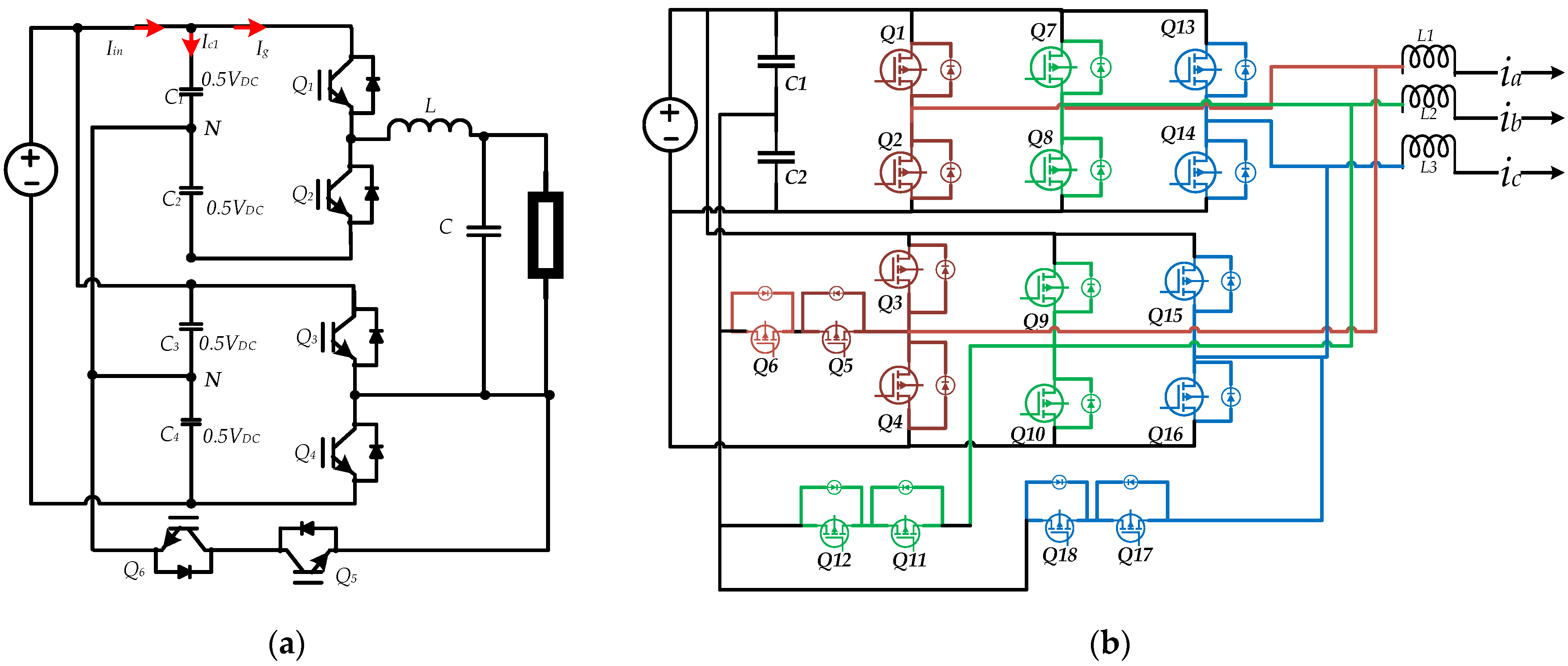
2. Proposed Topology

The proposed single-phase five-level inverter topology is shown in Figure 1a, and the three-phase five-level topology is shown in Figure 1b. For simplicity, we only analyze and simulate the single-phase circuit, but it can be extended to the three-phase circuit as shown in Figure 1b. In a single-phase circuit, six switches (preferably MOSFETs or IGBTs) and two flying capacitors are connected to a DC source, producing five voltage levels: VDC, 0.5VDC, 0, −VDC, −0.5VDC. A simple passive low-pass inductor-capacitor (LC) filter is used at the load side to mitigate the load current dynamics and prevent high frequency oscillations. In the proposed topology only two switches conduct current in each mode of operation, which reduces the switching losses and enhances the overall efficiency of the circuit. Moreover, each switch blocks a voltage of VDC/2 which reduces the cost of the switches as compared with two-level voltage inverters. Switches 1 and 2 operate at the modulation frequency while the other switches operate at the carrier frequency. Furthermore, the inverter gives zero output voltage at two separate states, which are efficiently used in one complete sinusoidal cycle to avoid extra dv/dt stresses on semiconductor switches. In addition, a DC neutral point at the center of the DC-link capacitors is connected to the load using a four-quadrant switch. As shown in Figure 1, the inverter has three legs and each leg consists of two semiconductors devices: upper (Q1, Q2), lower (Q3, Q4), and ground leg (Q5, Q6). The upper and lower legs are based on the half-bridge circuits while the grounded leg contains the two four-quadrant switches. For VDC and −VDC output voltages, the load is connected between the upper and the lower leg, while for VDC/2 and −VDC/2, the load is connected between the upper and the ground leg. The zero-output voltage is obtained by connecting the load to the higher or lower terminal of the upper and lower leg simultaneously.

2.1. Switching State Analysis

Six switches of the proposed topology are triggered in six different ways to get the five-level output. Six inverter stages attained by the different combinations of switches are shown in Figure 2.
There are two switching states that give zero output voltage. State five is used in the first half of the modulated sine wave, while the sixth state is used in the second half of the modulated sine wave. Switches Q1 & Q2, Q3 & Q4, and Q5 & Q6 are complementary to each other, and a dead time is defined between the transitions of these switches to avoid any short circuit. The operation of the proposed topology in different switching states is elaborated below and summarized in Table 1. The path of current in each switching state is shown with red lines in Figure 2, and the green line indicates zero current flow in that state.
(1)
State-1
In state-1, current flows from the positive terminal of the DC source to switch 1 and goes through the load to connect the circuit at the negative terminal of the DC source through switch 4, as shown in Figure 2a. Voltage appears across the load terminal in VDC.
(2)
State-2
In state-2, current starts flowing from the positive terminal of the DC source towards switch 1 and passes through the load to connect the circuit at the neutral point between the two DC link capacitors through switch 6, as shown in Figure 2c. The diode of switch 5 in this state behaves as if it were forward biased and conducts the current. Voltage appears at the load terminal in this state as VDC/2.
(3)
State-3
In state-3, current flows from the positive terminal of the DC source to switch 3 and goes through the negative potential of the load, completing the circuit at the negative terminal of the DC source through switch 2, as shown in Figure 2b. Negative voltage (−VDC) appears at the output.
(4)
State-4
In state-4, the positive terminal of the load is connected to the neutral point between DC link capacitors through switch 5 and the diode of switch 6, while the negative terminal of the load is connected to the negative terminal of the input source through switch 2. The diode of switch 6 will appear as forward bias in this state. It results in a −VDC/2 voltage appearing across the load terminals. The current path in this switching state is shown in Figure 2d.
(5)
State-5
To get the zero voltage at the load terminals, switches 1 and 3 will turn ON simultaneously. This will short the load terminals and the potential difference across them will be zero. The visualization of this state can be seen in Figure 2e. Additionally, in the future, the zero states can be used to run the inverter in a mode called “discontinuous conduction,” which keeps the size of the output passive filter small.
(6)
State-6
As in state 5, state 6 will also generate the zero voltage by turning switches 2 and 4 to the ON state. It will also make the potential difference in the output go to zero. Both states 5 and 6 are used effectively in the proposed topology. State 5 is used in the positive half of the modulated sine wave while the inverter goes into state 6 in the negative portion of the modulated sine wave when needed. Toggling states 5 and 6 in a single modulated sine wave cycle reduces switching dv/dt stresses.

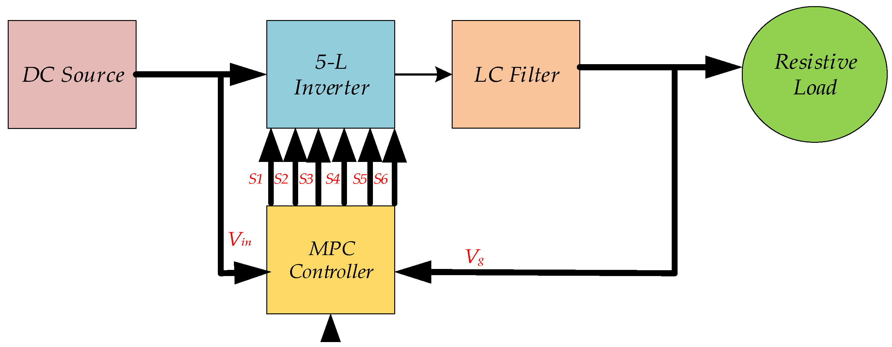
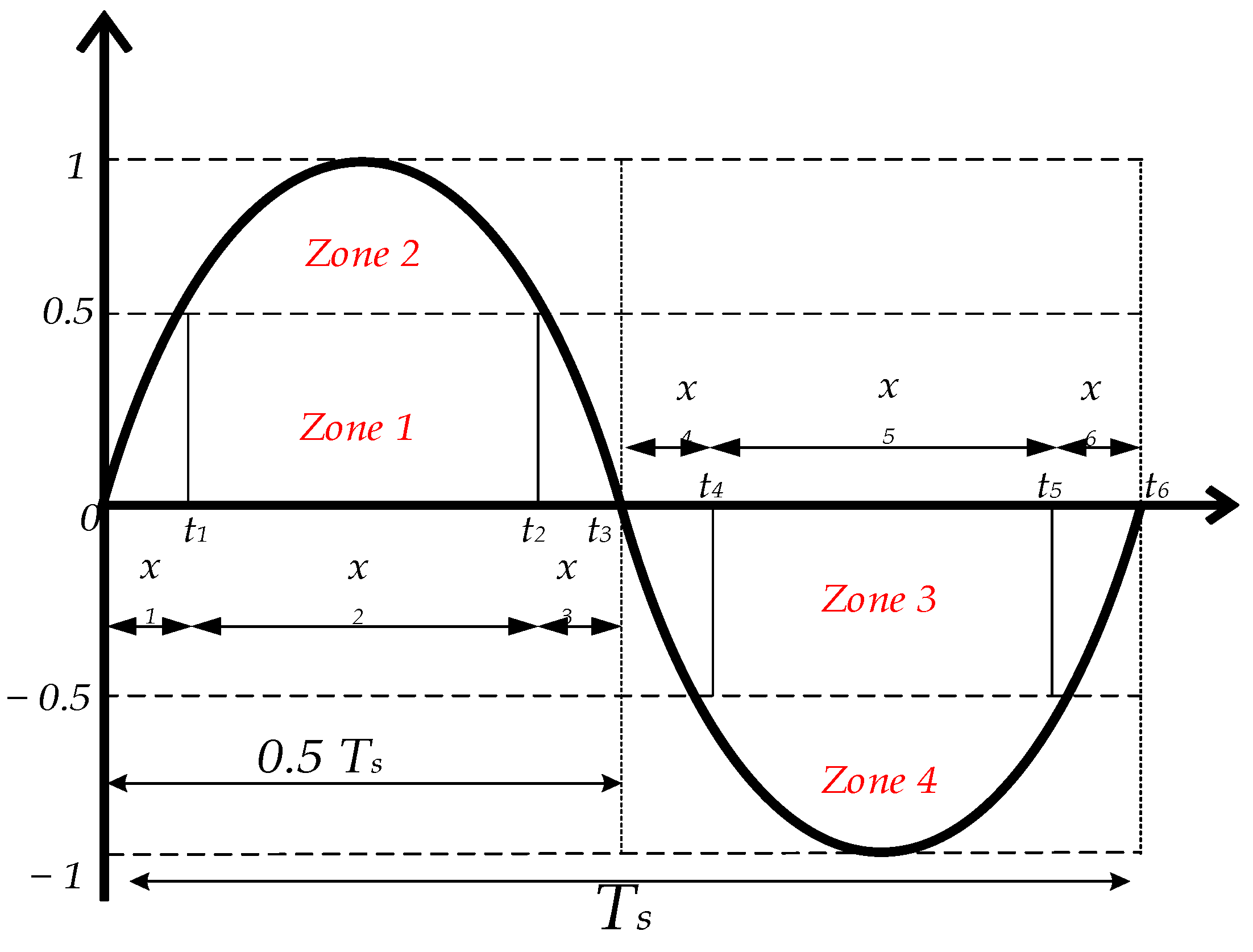
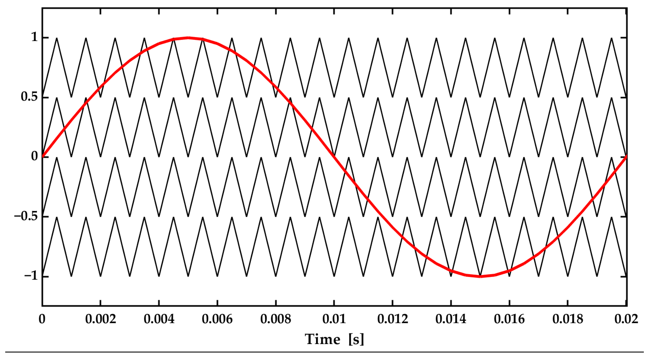
2.2. Controller Design for 5-Level Proposed Inverter

The design of the multilevel inverter controller is based on a modulation waveform that employs the switching states shown in Table 1. As illustrated in Figure 3, four triangular carrier signals are stacked with the sinusoidal modulation signal of the desired output frequency to regulate the PWM signal output. Figure 5 illustrates the division of the modulated sine wave into four different zones.
  • The switching signal oscillates between states 2 and 6 in the first zone of the modulation wave.
  • In the second region of the modulation wave, states 1 and 2 are used to form the switching signal.
  • The switching signal produced in the third section oscillates between states 4 and 5.
  • In the final portion of the modulation wave, signals will oscillate between states 3 and 4 for the generation of gate pulses.
Utilizing two distinct zero-voltage states during the positive and negative cycles of the modulation signal reduces switching strains and maintains voltage balance around the DC-link capacitors.

2.3. Inverter Output Controller

The multilevel voltage inverter is designed for a constant output voltage under variable input and output conditions. In this paper, a model predictive controller (MPC) is designed using the modulated sine wave to obtain constant output voltage under variable input/output voltage conditions. The system model is shown in Figure 4.
The modulated sine wave is divided into four zones and six time steps with respect to two reference points. The distance between two time steps is represented by the variable x, as shown in Figure 5, and their values are calculated using x1 and x3 which represent the time scales for zone 1 and 2, respectively. Similarly, for the negative signal, x4 and x6 are the times of zone 3, while x5 represents zone 4. For normal operation, the zone changing reference Zr is ±0.5. Increasing the value of Zr irrespective of the sign will decrease the output voltage and vice versa. The controller changes the value of Zr to keep the output voltage stable.
x 1 = t 1 = sin 1 y A × T s 360 x 3 = 180 sin 1 y A × T s 360 x 2 = x 3 x 1 x 4 = 180 + sin 1 y A × T s 360 x 6 = 360 sin 1 y A × T s 360 x 5 = x 6 x 5
In (1), y is the instantaneous value of modulated sine signal at time t1 and A is the amplitude of the modulated sine signal. Reference value Zr is used to select the instantaneous value y. Equation (1) is used to calculate the zone times of the modulation waveform.
By applying volt–sec balance for zone 1 and zone 2, the output voltage for one switching cycle is calculated using Equations (2) and (3) respectively.
Zone   1 :   V o = Z r × V i n × D
Zone   2 : V o = Z r × V i n × 1 + D
where Vo is the inverter output voltage, Vin is the input DC-link voltage, and D represents the switching duty ratio. The duty ratio follows the sinusoidal wave at every switching cycle. Zones 3 and 4 produce the same output voltage as zones 1 and 2, respectively, with a negative sign. The average voltage over zones 1 and 2 is calculated by summing all the output values in each switching cycle over the total number of values. The value will remain the same for zones 3 and 4 with a negative sign. We use one-half of the modulated sine wave to calculate the output sinusoidal voltage value. First, the average voltage in individual zones is calculated using (4) and (5) for the positive half of the modulated sine wave, i.e., zone 1 and zone 2. In the next step, these average voltages are summed up to obtain the total peak output value in the complete positive half of the modulated sine wave as illustrated in (6). The MPC controller will control this peak value to keep the output inverter voltage close to the reference value.
V 1 , a v g ( t ) = Z r ( t ) n × V i n n = 0 n = N 1 D ( n )             N 1 = f s × ( x 1 + x 3 )
V 2 , a v g ( t ) = 1 Z r ( t ) n × V i n 2 n = 0 n = N 2 1 + D ( n )
N 2 = f s × x 3
T s = 1 F o
Output Voltage at time t:
V o , a v g ( t ) = V 1 , a v g ( t ) + V 2 , a v g ( t )
where F 0 is the fundamental frequency of the inverter and Fs is the switching frequency of the inverter. N is the total number of switching cycles in one zone. The time step of the modulated sine wave is defined with t. Vo,peak is the inverter output voltage at time t, and is calculated using Equation (6). MPC will predict the output voltage for time t + 1 using the input value at t + 1 and zone reference value at time t using Equation (7).
Predicted output voltage at time t + 1;
V o , a v g * ( t + 1 ) = V 1 , a v g * ( t + 1 ) + V 2 , a v g * ( t + 1 )
where V o , a v g * is the predicted output voltage at time t + 1 with zone reference Z r * ( t ) and Vin(t + 1). The cost function (8) is minimized with iterative values of Zr. The iteration value for each iteration is set to 0.05 in our experiment. The value which minimizes the cost function will be the set zone reference for time t + 1. The flowchart of the MPC algorithm for output voltage control is illustrated in Figure 6.
  min Z r   V r e f V o , p e a k *   s . t             0.3 < Z r < 0.7
The iterative value of Zr to minimize the cost function follows two paths, if the cost function error is positive then the value of Zr will decrease and if the error is negative the value of Zr will increase This iteration continues until the minimal cost function is achieved.
To maintain the effectiveness of the 5-L inverter and the total harmonic distortion (THD) in the required range, the zone reference can be varied in a specified range. This range depends on the maximum allowable value of THD for the system. In this paper, the zone reference value is varied in the range of 0.3 to 0.7 to achieve THD less than 5%.

3. Loss Analysis

This section summarizes the calculation of conduction losses and the current/voltage stress on semiconductor devices considering the unity power factor. This paper will not undertake the switching analysis of the devices as it is similar to the one presented in the literature [30]. To simplify the loss analysis of the system, the duty cycles of each switch independent of the switching cycles of zones are taken from (9)–(13). Equations are derived for one complete sinusoidal cycle using work from the literature [30,31].
V H d 1 t + V L d 2 t = 2 d t V D C d 1 t + d 2 t = 1
where VH and VL are the high and low voltages in one duty cycle, and 2d(t)VDC is the function of the inverter output.
d 1 ( t ) = 2 d t d 2 t = 1 2 d t Zone     1
d 1 t = 4 d t 1 d l 2 t = 2 4 d t Zone   2
d 1 ( t ) = 2 d t d 2 t = 1 + 2 d t Zone       3
d 1 t = 4 d t 1 d 2 t = 2 + 4 d t Zone   4
The time cycles of all the zones are calculated using (1). The conduction losses of the switches involved in each zone over a period of T are calculated as
P c o n d = 1 T o T V o n × d i × i o           i = 1 , 2...6
where Pcond is the power conduction loss, Von is the voltage drop of the switch during the ON state, which is available in the datasheet and calculated using (14). Io is the current flowing through the switch during cycle di, where i indicates the switch duty ratio as shown in Table 2.

4. Simulation and Experimental Results

The simulation and experimental results were carried out using MATLAB/Simulink and DSPACE controller. A comparison of the number of active and passive components used in the topology with previously proposed topologies is summarized in Table 3. It can be seen that the proposed topology uses a lesser number of components to produce five-level inverter output.

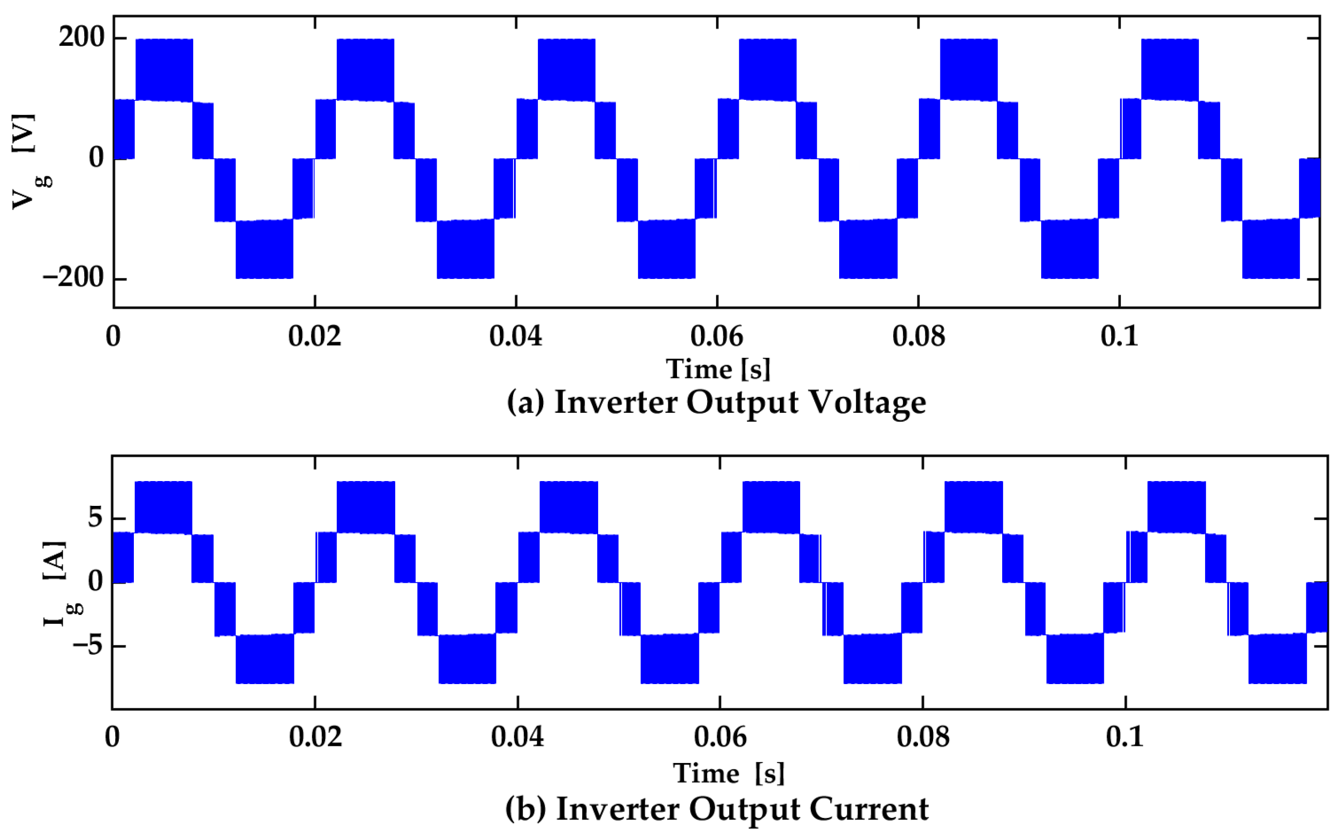
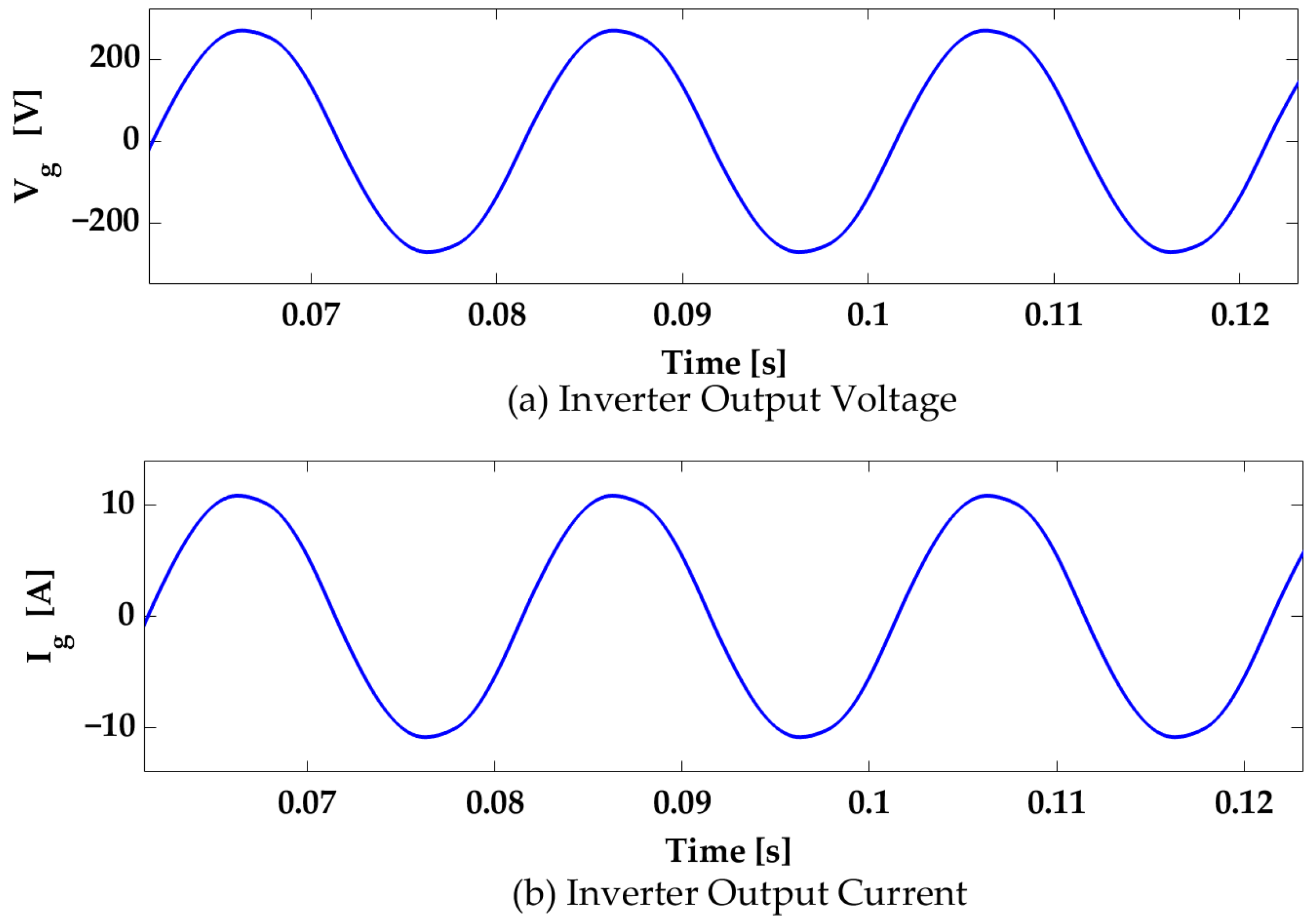
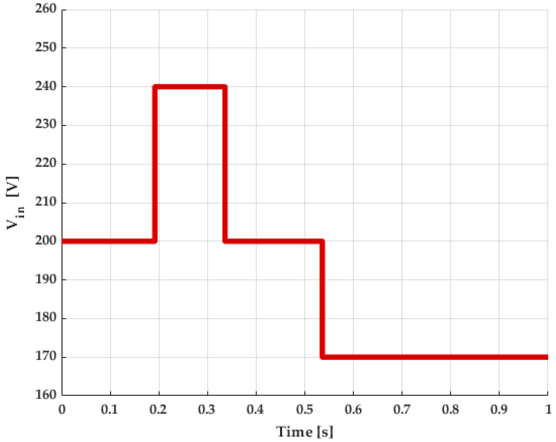
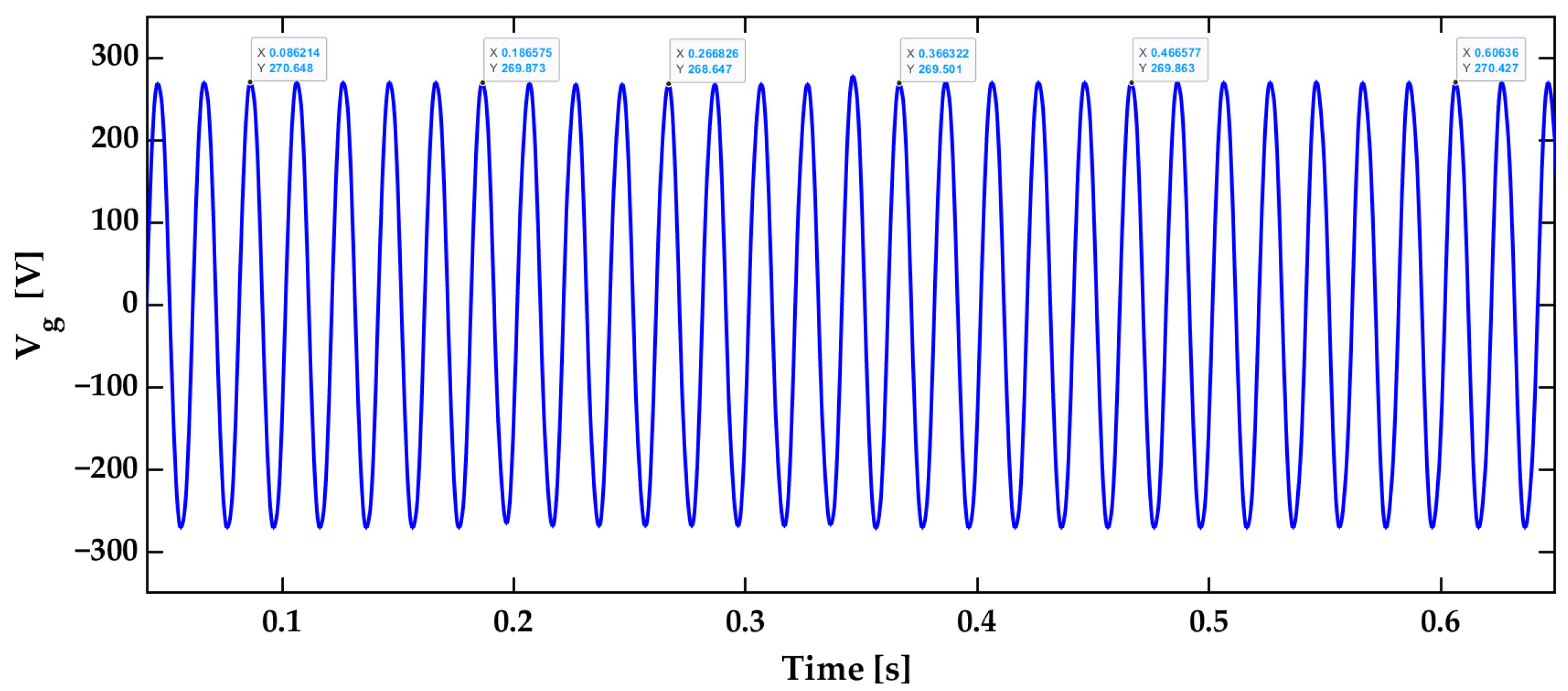
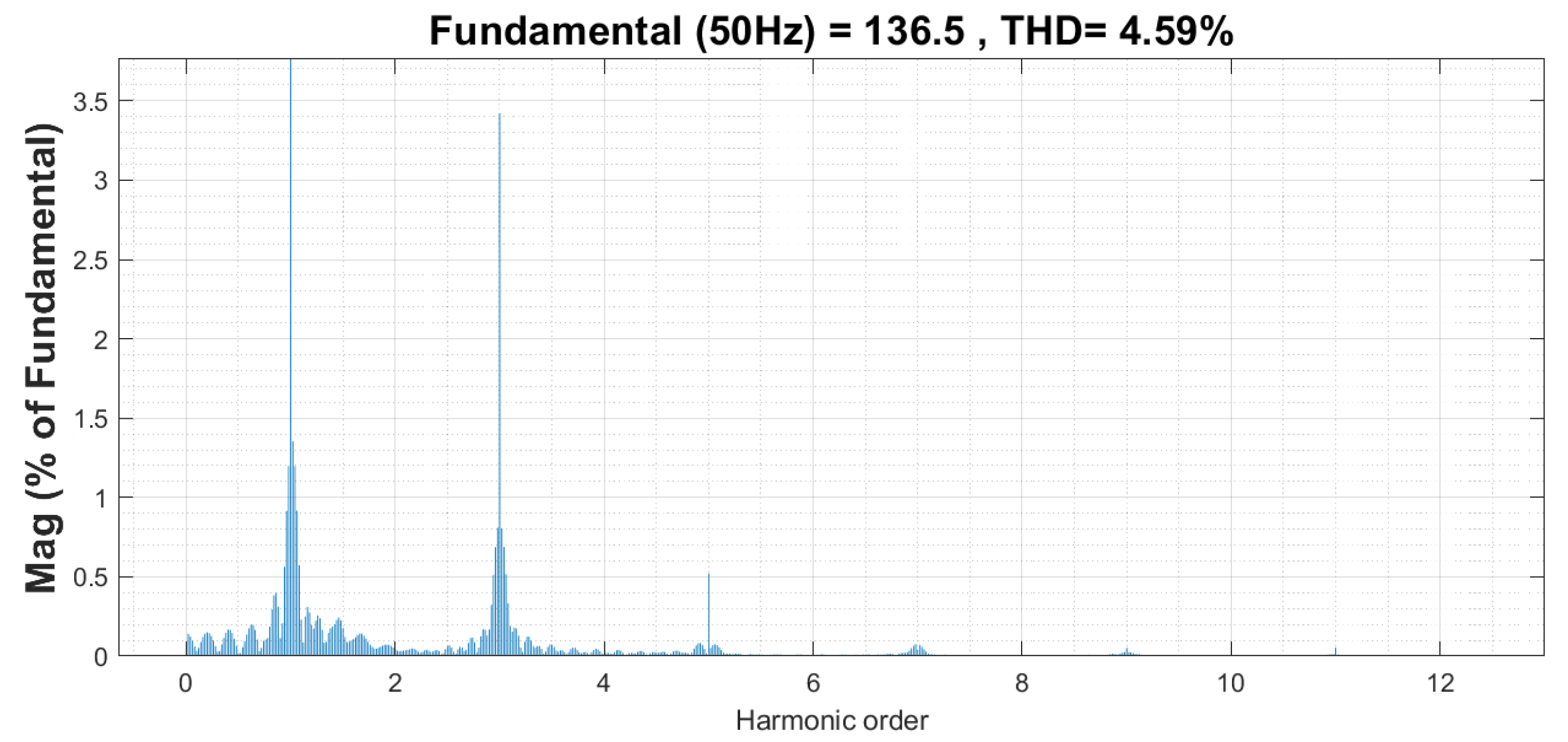
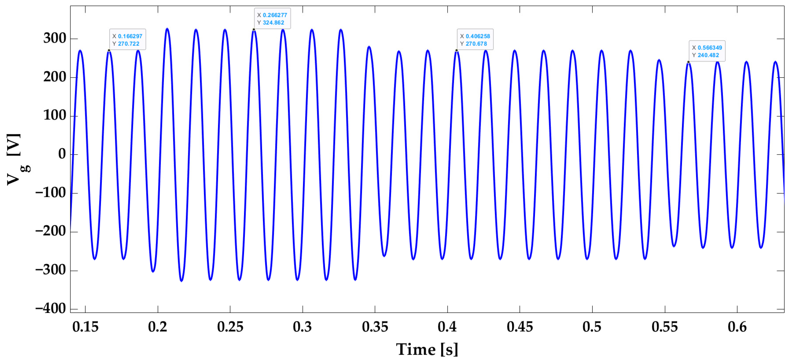
4.1. Simulation Results

The validation of the proposed 5-level voltage source inverter was tested using discrete time-based simulations on MATLAB/Simulink software. The system parameters used in the validation process are listed in Table 4.
Three simulation results were carried out to prove the feasibility and performance of the proposed inverter. In the first test, the output waveform was generated without a filter and control algorithm to verify the 5-level inverter response with a fixed input voltage of 200 V. The resistive load of 50-Ω is attached to the inverter output to obtain waveforms. Figure 7 shows the conventional five-level voltage and current output inverter waveforms without filter [24]. All results were generated at a 10 kHz frequency with a modulation index of 1.
The second test was performed with the addition of an LC filter in the circuit to obtain a pure sinusoidal output waveform and decrease the THD in the circuit. The input voltage was fixed at 200 V and the resistive load of 50-Ω was attached to the output of the circuit. The inductor and capacitor values of the LC filter were 3 mH and 30 µF, respectively.
Figure 8 shows the pure sinusoidal waveform obtained with the LC filter. Harmonics in the output waveform is reduced and FFT analysis is undertaken to calculate THD as shown in Figure 9.
In the third setup, the MPC controller was added to the circuit. Two voltage sensors were attached to feed voltage measurements to the controller from the input and output of the circuit. The maximum acceptable change in the input voltage was 20% to keep the THD less than 5%. Therefore, the input voltage was varied from 170 V to 240 V at four different timestamps as shown in Figure 10. The sampling time of the circuit was set to 0.00001 s. The simplicity of the controller circuit decreases the response time of the circuit toward any change in the input voltage.
The controller output signal was given to the PWM generator. At each timestamp, the output voltage was predicted with respect to the input voltage using (7). As long as the input voltage is equal to the reference voltage, the controller output is maintained at 0.5 value. The reference signal at the controller output changes along with the change in inverter output voltage and begins to change in small steps. At each step, the new output voltage was predicted, and the signal adjusted accordingly. At 0.2 sec, the input voltage was equal to the reference signal and the controller signal jumped from a 0.7 to a 0.5 value. At 0.1 and 0.3 the controller output increased and decreased in small steps.
Figure 11 shows the output voltage of the inverter with a controlled modulation signal. The output voltage was kept in the range of 268 V to 270 V by the controller. The output voltage remained at 269 V when the input voltage was varied between 170 V to 240 V. Figure 12 shows the inverter voltage without a controller. The output voltage varied between 240 V to 324 V against the same varied input voltage. This huge variation in output voltage value increased the THD to 11.2%, which is more than double the value of the accepted international standard value of THD.
The LC filter remains the same during the controlled and uncontrolled modulation technique, which affects the THD of the system. For the controlled modulation technique, the zone reference was varied between 0.3 to 0.7 to keep the THD in the allowable range (THD < 5%). If the zone reference is not kept in the limited range, the THD exceeds the allowable value and affects the system’s performance. If the LC filter is variable and controlled by a controller, then the zone reference can be varied from 0 to 1. With the zone reference value of zero or one, the inverter will behave as a three-level inverter. The THD of the controlled output voltage inverter is 4.59% and the FFT analysis graph is shown in Figure 13.

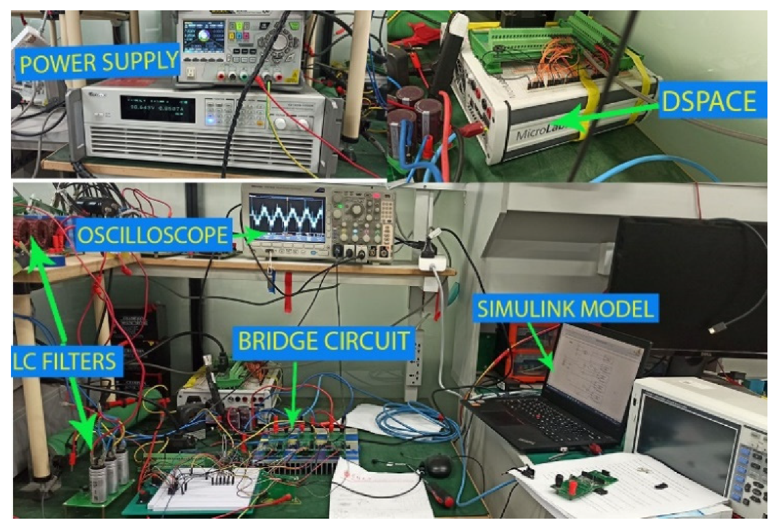
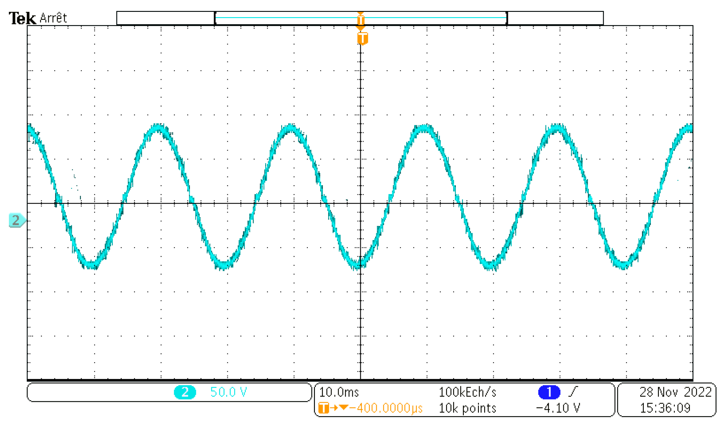
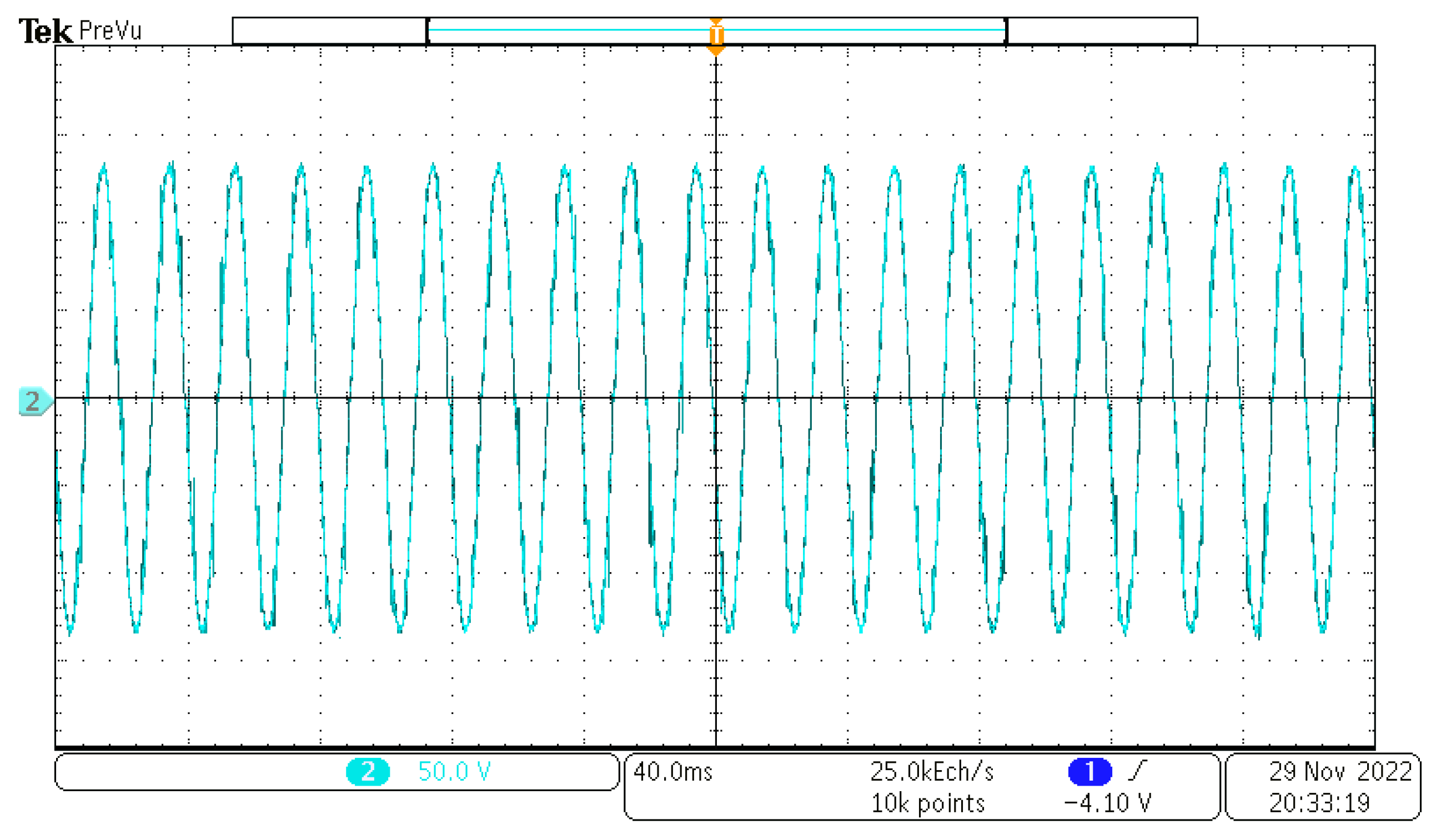
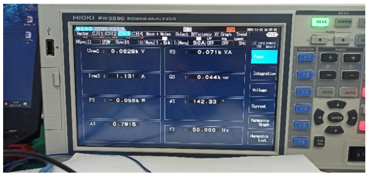
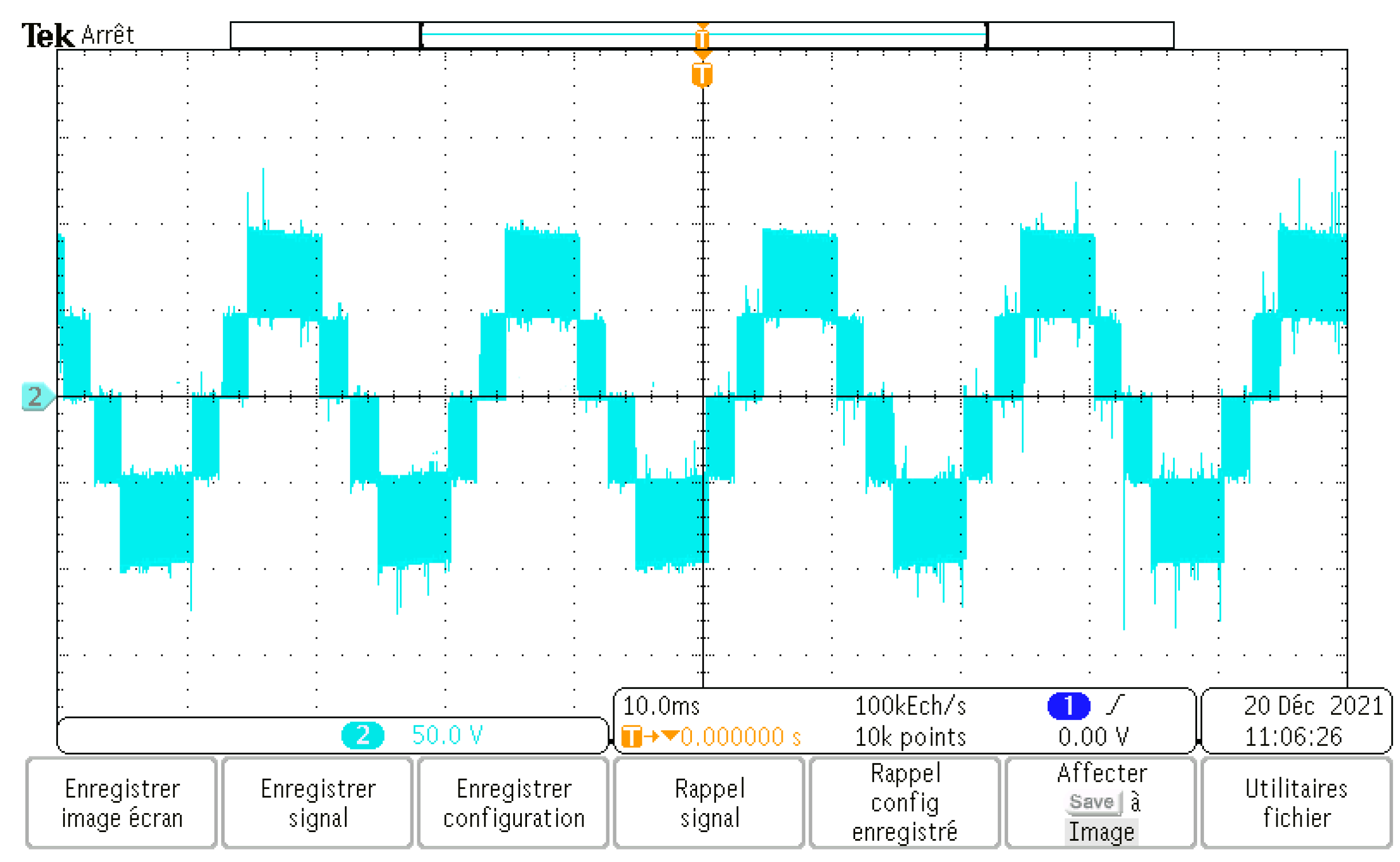
4.2. Experimental Results

A laboratory prototype of the proposed 5-level inverter topology was developed for experimental verification as shown in Figure 14. Six IHW15N120E1 IGBTs were used as power switches and the switching modulation signals were controlled using a DSPACE controller fed through a MATLAB/Simulink model. The dead time of 1 µs was provided in DSPACE for the complimentary switches and the switching frequency was set to 10 kHz for all switches. Three half-bridge circuits were connected to build the proposed topology and are collectively called the bridge circuit in Figure 15. The main power supply was used to give the input power to the circuit, calibrated at 100 V and 2 A. The smaller power supply was used to supply power to the gate driving circuit.
A resistive load of 50 Ω was attached to the output of the inverter. Figure 15 shows the conventional five-level inverter output without an LC filter at 100 V input voltage. A second test was performed by connecting the LC filter in the circuit and Figure 16 shows the output voltage of the inverter using the designed LC filter. In the third step, the sensors were attached in the circuit and their output was fed to the Dspace controller to control the output voltage using MPC. The MPC model was designed in the MATLAB and the signal communicated from the hardware circuit through Dspace. The controlled output voltage using MPC controller is shown in Figure 17. The hardware setup waveforms were captured using an oscilloscope. The input power was obtained from the main power supply and the output power was measured using a power analyzer as shown in Figure 18. The overall efficiency was calculated by using the values of the power analyzer for the hardware prototype, which was determined to be 91.7%.

4.3. Discussion

Simulation and hardware findings demonstrate that the proposed 5-level inverter topology and voltage controller outperform the existing NPC and T-type 5-level inverter topologies and their controllers with respect to voltage stability and efficiency. This is due to the way that the decrease switches in the architecture use the modulation signal to stabilize the output voltage, lower the THD and boost the inverter’s overall efficiency. Moreover, it is important to note that the primary function of the controller is to alter the inverter operating time in line with the dc-link voltage. The capability of the suggested controller to run the inverter in five as well as three voltage levels is advantageous for regulating the output voltage with reduced THD.

5. Conclusions

This paper proposed a novel topology and control circuit for a five-level inverter with a reduced number of components. Six switches operated in six different states to generate a five-level output. Only two switches operated in a single state, reducing the stress on the switches. The modulation technique was divided into four zones and the zone time was controlled with a model predictive controller to manage the power switches and maintain a consistent output voltage despite variable input voltage. The THD remains less than 5% regardless of the input voltage. The proposed control circuit design is both simpler and more efficient. Using a power analyzer, the efficiency of the hardware circuit is calculated 91.7%.

Author Contributions

Conceptualization, M.A.A. and Y.L.; methodology, M.A.A.; software, M.A.A.; validation, M.A.A., J.P. and Y.L.; writing—original draft preparation, M.A.A. and Y.L.; writing—review and editing, S.A., J.Y. and J.P.; supervision, J.P. and Y.L.; project administration, J.P. and Y.L.; funding acquisition, J.Y. and Y.L. All authors have read and agreed to the published version of the manuscript.

Funding

This research was funded by the Foundation of Shenzhen Science and Technology under grant number JCYJ20200109105204077.

Conflicts of Interest

The authors declare no conflict of interests.

References

  1. Shi, Y.; Wang, L.; Xie, R.; Shi, Y.; Li, H. A 60-kW 3-kW/kg Five-Level T-Type SiC PV Inverter With 99.2% Peak Efficiency. IEEE Trans. Ind. Electron. 2017, 64, 9144–9154. [Google Scholar] [CrossRef]
  2. Gultekin, B.; Ermis, M. Cascaded Multilevel Converter-Based Transmission STATCOM: System Design Methodology and Development of a 12 kV ±12 MVAr Power Stage. IEEE Trans. Power Electron. 2013, 28, 4930–4950. [Google Scholar] [CrossRef]
  3. Wang, H.; Kou, L.; Liu, Y.-F.; Sen, P.C. A Seven-Switch Five-Level Active-Neutral-Point-Clamped Converter and Its Optimal Modulation Strategy. IEEE Trans. Power Electron. 2017, 32, 5146–5161. [Google Scholar] [CrossRef]
  4. Itoh, Y.K.J.; Itoh, J. Performance Evaluation among Four types of Five-level Topologies using Pareto Front Curves. In Proceedings of the 2013 IEEE Energy Conversion Congress and Exposition, Denver, CO, USA, 15–19 September 2013; pp. 1296–1303. (In English). [Google Scholar]
  5. Wang, K.; Zheng, Z.; Li, Y.; Liu, K.; Shang, J. Neutral-Point Potential Balancing of a Five-Level Active Neutral-Point-Clamped Inverter. IEEE Trans. Ind. Electron. 2012, 60, 1907–1918. [Google Scholar] [CrossRef]
  6. Rodriguez, J.; Bernet, S.; Steimer, P.K.; Lizama, I.E. A Survey on Neutral-Point-Clamped Inverters. IEEE Trans. Ind. Electron. 2010, 57, 2219–2230. [Google Scholar] [CrossRef]
  7. Shuvo, S.; Hossain, E.; Islam, T.; Akib, A.; Padmanaban, S.; Khan, Z.R. Design and Hardware Implementation Considerations of Modified Multilevel Cascaded H-Bridge Inverter for Photovoltaic System. IEEE Access 2019, 7, 16504–16524. [Google Scholar] [CrossRef]
  8. Kuncham, S.K.; Annamalai, K.; Subrahmanyam, N. A Two-Stage T-Type Hybrid Five-Level Transformerless Inverter for PV Applications. IEEE Trans. Power Electron. 2020, 35, 9510–9521. [Google Scholar] [CrossRef]
  9. Zhang, L.; Zheng, Z.; Li, C.; Ju, P.; Wu, F.; Gu, Y.; Chen, G. A Si/SiC Hybrid Five-Level Active NPC Inverter with Improved Modulation Scheme. IEEE Trans. Power Electron. 2019, 35, 4835–4846. [Google Scholar] [CrossRef]
  10. Yu, H.; Chen, B.; Yao, W.; Lu, Z. Hybrid Seven-Level Converter Based on T-Type Converter and H-Bridge Cascaded Under SPWM and SVM. IEEE Trans. Power Electron. 2017, 33, 689–702. [Google Scholar] [CrossRef]
  11. Baker. High Voltage Converter Circuit. United States, 1980.
  12. Meynard, T.; Fadel, M.; Aouda, N. Modeling of Multilevel Converters. IEEE Trans. Ind. Electron. 1997, 44, 356–364. [Google Scholar] [CrossRef]
  13. Zhao, Z.; Zhao, J.; Huang, C. An Improved Capacitor Voltage-Balancing Method for Five-Level Diode-Clamped Converters with High Modulation Index and High Power Factor. IEEE Trans. Power Electron. 2015, 31, 3189–3202. [Google Scholar] [CrossRef]
  14. Meynard, T.A.; Foch, H. Multi-Level Conversion High Voltage Choppers and Voltage Source Inverters. In Proceedings of the PESC '92 Record. 23rd Annual IEEE Power Electronics Specialists Conference, Toledo, Spain, 29 June–3 July 1992. [Google Scholar]
  15. Salinas, F.; Gonzalez, M.A.; Escalante, M.F.; Morales, J.D.L. Control Design Strategy for Flying Capacitor Multilevel Converters Based on Petri Nets. IEEE Trans. Ind. Electron. 2015, 63, 1728–1736. [Google Scholar] [CrossRef]
  16. Omer, P.; Kumar, J.; Surjan, B.S. A Review on Reduced Switch Count Multilevel Inverter Topologies. IEEE Access 2020, 8, 22281–22302. [Google Scholar] [CrossRef]
  17. Wu, P.-H.; Chen, Y.-T.; Cheng, P.-T. The Delta-Connected Cascaded H-Bridge Converter Application in Distributed Energy Resources and Fault Ride Through Capability Analysis. IEEE Trans. Ind. Appl. 2017, 53, 4665–4672. [Google Scholar] [CrossRef]
  18. Schweizer, M.; Kolar, J.W. Design and Implementation of a Highly Efficient Three-Level T-Type Converter for Low-Voltage Applications. IEEE Trans. Power Electron. 2012, 28, 899–907. [Google Scholar] [CrossRef]
  19. Bruckner, T.; Bernet, S. Loss balancing in three-level voltage source inverters applying active NPC switches. In Proceedings of the 32nd Annual Power Electronics Specialists Conference, Vancouver, BC, Canada, 17–21 June 2001; Volume 1–4, pp. 1135–1140. (In English). [Google Scholar]
  20. Bharath, G.V.; Hota, A.; Agarwal, V. A New Family of 1-Five-Level Transformerless Inverters for Solar PV Applications. IEEE Trans. Ind. Appl. 2019, 56, 561–569. [Google Scholar] [CrossRef]
  21. Davis, T.T.; Dey, A. A Neutral Point Voltage Balancing Scheme with Improved Transient Performance for 5-Level ANPC and TNPC Inverters. IEEE Trans. Power Electron. 2019, 34, 12513–12523. [Google Scholar] [CrossRef]
  22. Vujacic, M.; Dordevic, O.; Grandi, G. Evaluation of DC-Link Voltage Switching Ripple in Multiphase PWM Voltage Source Inverters. IEEE Trans. Power Electron. 2019, 35, 3478–3490. [Google Scholar] [CrossRef]
  23. Zhang, Y.; Qu, C. Model Predictive Direct Power Control of PWM Rectifiers Under Unbalanced Network Conditions. IEEE Trans. Ind. Electron. 2015, 62, 4011–4022. [Google Scholar] [CrossRef]
  24. Siddique, M.D.; Bhaskar, M.S.; Rawa, M.; Mekhilef, S.; Memon, M.A.; Padmanaban, S.; Almakhles, D.J.; Subramaniam, U. Single-phase hybrid multilevel inverter topology with low switching frequency modulation techniques for lower order harmonic elimination. IET Power Electron. 2020, 13, 4117–4127. [Google Scholar] [CrossRef]
  25. Bozorgi, A.M.; Gholami-Khesht, H.; Farasat, M.; Mehraeen, S.; Monfared, M. Model Predictive Direct Power Control of Three-Phase Grid-Connected Converters with Fuzzy-Based Duty Cycle Modulation. IEEE Trans. Ind. Appl. 2018, 54, 4875–4885. [Google Scholar] [CrossRef]
  26. Bouafia, A.; Gaubert, J.-P.; Krim, F. Predictive Direct Power Control of Three-Phase Pulsewidth Modulation (PWM) Rectifier Using Space-Vector Modulation (SVM). IEEE Trans. Power Electron. 2009, 25, 228–236. [Google Scholar] [CrossRef]
  27. Bouafia, A.; Krim, F.; Gaubert, J.-P. Fuzzy-Logic-Based Switching State Selection for Direct Power Control of Three-Phase PWM Rectifier. IEEE Trans. Ind. Electron. 2009, 56, 1984–1992. [Google Scholar] [CrossRef]
  28. Khan, S.A.; Guo, Y.; Zhu, J. Model Predictive Observer Based Control for Single-Phase Asymmetrical T-Type AC/DC Power Converter. IEEE Trans. Ind. Appl. 2018, 55, 2033–2044. [Google Scholar] [CrossRef]
  29. Choi, D.-K.; Lee, K.-B. Dynamic Performance Improvement of AC/DC Converter Using Model Predictive Direct Power Control with Finite Control Set. IEEE Trans. Ind. Electron. 2014, 62, 757–767. [Google Scholar] [CrossRef]
  30. Grigoletto, F.B. Five-Level Transformerless Inverter for Single-Phase Solar Photovoltaic Applications. IEEE J. Emerg. Sel. Top. Power Electron. 2019, 8, 3411–3422. [Google Scholar] [CrossRef]
  31. Barzegarkhoo, R.; Siwakoti, Y.P.; Blaabjerg, F. A New Switched-Capacitor Five-Level Inverter Suitable for Transformerless Grid-Connected Applications. IEEE Trans. Power Electron. 2020, 35, 8140–8153. [Google Scholar] [CrossRef]
  32. Rahul S, A.; Pramanick, S.; Kaarthik, S.; Gopakumar, K.; Blaabjerg, F. Extending the Linear Modulation Range to the Full Base Speed Using a Single DC-Link Multilevel Inverter with Capacitor-Fed H-Bridges for IM Drives. IEEE Trans. Power Electron. 2016, 32, 5450–5458. [Google Scholar] [CrossRef]
  33. Dao, N.D.; Lee, D.-C. Operation and Control Scheme of a Five-Level Hybrid Inverter for Medium-Voltage Motor Drives. IEEE Trans. Power Electron. 2018, 33, 10178–10187. [Google Scholar] [CrossRef]
  34. Majumder, M.G.; R, R.; Gopakumar, K.; Umanand, L.; Al-Haddad, K.; Jarzyna, W. A Fault-Tolerant Five-Level Inverter Topology with Reduced Component Count for OEIM Drives. IEEE J. Emerg. Sel. Top. Power Electron. 2020, 9, 961–969. [Google Scholar] [CrossRef]
  35. Dargahi, V.; Sadigh, A.K.; Corzine, K.A.; Enslin, J.H.; Rodriguez, J.; Blaabjerg, F. A New Control Technique for Improved Active-Neutral-Point-Clamped (I-ANPC) Multilevel Converters Using Logic-Equations Approach. IEEE Trans. Ind. Appl. 2019, 56, 488–497. [Google Scholar] [CrossRef]
Figure 1. (a) 5-L single-phase inverter topology, (b) 5-L three-phase inverter topology.
Sustainability 15 00860 g001
Figure 2. Different output voltage states: (a) Vg = VDC, (b) Vg = −VDC, (c) Vg = VDC/2, (d) Vg = −VDC/2, and (e) Vg = 0 (f) Vg = 0.
Sustainability 15 00860 g002
Figure 3. Four carrier signals of 1 kHz and one modulation signal at 50 Hz.
Sustainability 15 00860 g003
Figure 4. Level inverter with MPC controller.
Sustainability 15 00860 g004
Figure 5. Demonstration of modulation signal use to control the output voltage.
Sustainability 15 00860 g005
Figure 6. Flow chart of model predictive control.
Sustainability 15 00860 g006
Figure 7. (a) Output voltage and (b) current waveforms without Filter.
Sustainability 15 00860 g007
Figure 8. Output inverter waveform with filter.
Sustainability 15 00860 g008
Figure 9. FFT analysis of the inverter output voltage with filter.
Sustainability 15 00860 g009
Figure 10. Varied input voltage used in the simulation circuit.
Sustainability 15 00860 g010
Figure 11. Controlled output voltage.
Sustainability 15 00860 g011
Figure 12. Inverter output voltage without controller.
Sustainability 15 00860 g012
Figure 13. FFT analysis of controlled voltage inverter.
Sustainability 15 00860 g013
Figure 14. Hardware prototype for the proposed topology.
Sustainability 15 00860 g014
Figure 15. Five level inverter output without filter.
Sustainability 15 00860 g015
Figure 16. Inverter output voltage with LC filter.
Sustainability 15 00860 g016
Figure 17. Controlled 5-level inverter output voltage.
Sustainability 15 00860 g017
Figure 18. Output measurements recorded by power analyzer.
Sustainability 15 00860 g018
Table 1. Switching states of proposed inverter.
Output (Vo)Q1Q2Q3Q4Q5Q6
State-1VDC100100
State-2VDC/2100001
State-3−VDC011000
State-4−VDC/2010010
State-50101000
State-60010100
Table 2. Duty cycles of switches in each zone.
SwitchesZone 1Zone 2Zone 3Zone 4
S12d(t)4d(t) − 100
S200−2d(t)−4d(t) − 1
S30002 + 4d(t)
S402 − 4d(t)00
S5001 + 2d(t)0
S61 − 2d(t)000
Table 3. Comparison of device count for different 5-level inverters.
TopologySwitch CountCapacitorsClamping DiodesDC Sources
Proposed6401
5-L inverter [32]10601
Hybrid 5-L [33]8303
NPC 5-L80124
FC 5-L81801
Standard ANPC8301
CHB 5-L8006
5-L Inverter [34]8401
5L-Improved ANPC [35]10002
Table 4. System parameters.
S. NoParametersValue
1Power Rating1000 watts
2Input Voltage200 V
3AC output Voltage200 V
4Switching Frequency10 kHz
5DC-Link Capacitors470 µF
6Filter Inductors3 mH
7Filter Capacitors30 µF
8Load Resistor50 Ω
Disclaimer/Publisher’s Note: The statements, opinions and data contained in all publications are solely those of the individual author(s) and contributor(s) and not of MDPI and/or the editor(s). MDPI and/or the editor(s) disclaim responsibility for any injury to people or property resulting from any ideas, methods, instructions or products referred to in the content.

