Article

CoO, Cu, and Ag Nanoparticles on Silicon Nanowires with Photocatalytic Activity for the Degradation of Dyes

by
Olda Alexia Cárdenas Cortez
1,2,
José de Jesús Pérez Bueno
1,*,
Yolanda Casados Mexicano
1,
Maria Luisa Mendoza López
3,
Carlos Hernández Rodríguez
1,
Alejandra Xochitl Maldonado Pérez
1,
David Cruz Alejandre
2,
Coraquetzali Magdaleno López
1,4,
María Reina García Robles
1,
Goldie Oza
1,
José Germán Flores López
1 and
Hugo Ruiz Silva
1
1
Centro de Investigación y Desarrollo Tecnológico en Electroquímica, S. C., Parque Tecnológico Querétaro-Sanfandila, Pedro Escobedo, Querétaro C.P. 76703, Mexico
2
Tecnológico Nacional de México, Instituto Tecnológico Superior de Poza Rica. lll Ver, Luis Donaldo Colosio s/n, Ejido Arroyo del Maíz, Poza Rica de Hidalgo, Veracruz C.P. 93230, Mexico
3
Tecnológico Nacional de México, Instituto Tecnológico de Querétaro, Av. Tecnológico s/n Esq. M. Escobedo Col. Centro, Querétaro C.P. 76000, Mexico
4
Centro de Investigación y de Estudios Avanzados del Instituto Politécnico Nacional, Unidad Saltillo, Av. Industria Metalúrgica No. 1062, Parque Industrial, Ramos Arizpe, Coahuila C.P. 25900, Mexico
*
Author to whom correspondence should be addressed.
Sustainability 2022, 14(20), 13361; https://doi.org/10.3390/su142013361
Submission received: 25 June 2022 / Revised: 27 September 2022 / Accepted: 30 September 2022 / Published: 17 October 2022
(This article belongs to the Special Issue Frontiers in Nanomaterials Utilization in Water Treatment)

Abstract

:
Photocatalytic semiconductors require maintaining stability and pursuing higher efficiencies. The studied systems were silicon nanowires (SiNWs), silicon nanowires with cobalt oxide nanoparticles (SiNWs-CoONPs), and silicon nanowires with copper nanoparticles (SiNWs-CuNPs). SiNWs were synthesized by metal-assisted chemical etching (MACE) from silicon wafers keeping the remaining silver nanoparticles for all three sample types. The nanowires were about 23–30 µm in length. CoONPs and CuNPs were deposited on SiNWs by the autocatalytic reduction processes (electroless). There were many factors in the process that affect the resulting structures and degradation efficiencies. This work shows the degradation of methyl orange (MO) together with the chemisorption of methylene blue (MB), and rhodamine 6G (Rh6G) by direct illumination with visible radiation. The MO degradation kinetics were in the sequence SiNWs-CuNPs (88.9%) > SiNWs (85.3%) > SiNWs-CoONPs (49.3%), with the SiNWs-CuNPs having slightly faster kinetics. However, SiNWs-CoONPs have slow degradation kinetics. The chemisorptions of MB and Rh6G were SiNWs-CuNPs (87.2%; 86.88%) > SiNWs (86%; 87%) > SiNWs-CoONPs (17.3%; 12%), showing dye desorptions together with lower chemisorption capacities. This work shows iridescence in optical microscopy images by the visible light interference caused by the spaces between the nanowire bundles.

1. Introduction

In recent years, soil, air, and water bodies have been the primary concern due to the alarming increment of their contamination. Pollution comes mainly from pesticides, heavy metals, and dyes, causing severe damage to human health and altering the ecological equilibrium. Thus, quantifying these pollutants and their removal is important for protecting human wellness and environmental conservation [1]. Nowadays, the trend is to develop new technologies and materials capable of facing environmental contamination and being at the same time eco-friendly and sustainable.
The textile industry is important for many nations because materials, assembled parts, or final products are generally exported to the United States of America and the European Union. However, the textile industry contributes the most to environmental deterioration due to a large amount of water used, later converted into wastewater with a high content of harmful chemicals to humans and the ecosystems. In this industry, dyes are challenging compounds to remove from sewage because they are present in ppm concentrations and are hardly biodegradable. Azo dyes are some of the priority dyes to remove from wastewater due to their release of chemicals. They have already been banned in the European Union. Therefore, the treatment of colored effluents becomes an issue of environmental concern. The techniques used to treat dyes in wastewater are the Fenton processes [2,3], ozonation [4], adsorption [4,5,6,7,8], membrane technology [4,9,10], electrochemical techniques [10], photocatalysis [11,12,13], and others [14,15,16].
Heterogeneous photocatalysis with nanostructured semiconductors has become an up-and-coming innovative technique due to its unique structures and properties [11]. This is the case with silicon nanowires [12,17,18,19,20,21], a nanostructure proving to be an effective photocatalyst for the oxidation of organic dyes and aromatic molecules, which exhibit higher efficiency if they are decorated with metallic nanoparticles. Here, efficiency is assumed as the conversion rate of radiative energy into breakage of atomic bonds of the pollutant molecules by transforming photons into electron–hole pairs and then into reactive oxygen species. Previous works have demonstrated the efficacy of silicon nanowires decorated with copper nanoparticles in degrading organic dyes, such as methyl orange, and reducing other chemicals, such as chromium, using visible light [12]. This, even considering that silicon in bulk is not a photocatalyst because it does not have the conduction band potential to generate OH radicals or even hydrogen peroxide. Another drawback of this nanostructured silicon with Schottky barriers is its efficiency reduction in consecutive photocatalysis cycles attributed to the increased copper oxide layer around the nanoparticles. Nonetheless, silicon is the most used semiconductor in the electronic industry and is broadly used in photovoltaics. Improving its efficiencies could make photocatalysis a feasible method of water and air treatments.
The cobalt oxides CoO and Co3O4 [22,23], among other oxides such as TiO2, ZnO, or CuO, have been profusely investigated for their catalytic activities in the oxidative degradation of organic pollutants [11,13,24,25,26,27,28]. In addition, their catalytic activities have been analyzed for water splitting [24,25,29,30,31], showing an oxygen evolution reaction and CO2 reduction, conducting to obtaining species, such as CH4 [32,33].
Aligned with the above topics, methyl orange (MO) [1,34,35], methylene blue (MB) [15,36,37,38,39], and rhodamine 6G (Rh6G) [16,34,40,41,42,43] are dyes frequently used to evaluate the photocatalytic activity of some semiconductors and other compounds, such as TiO2, ZnO, or reduced graphene oxide [11,13,26].
This work consists of depositing cobalt to obtain cobalt oxide nanoparticles on the silicon nanowires to cause a reduction of organic dyes using photocatalysis with visible irradiation. The proposal for cobalt oxide nanoparticles instead of copper is that cobalt oxide has been reported as photocatalytic and is already stable when exposed to oxygen from the environment, making it an excellent candidate to be stable in consecutive photocatalysis cycles. The organic dyes studied were methyl orange, methylene blue, and rhodamine 6G in a concentration of 20 ppm. The silicon nanowires were synthesized by metal-assisted etching (MACE), while the cobalt oxide nanoparticles were deposited by the electroless technique on the nanowires.

2. Materials and Methods

2.1. Preparation of the Silicon Wafers

The monocrystalline p-type silicon c-Si wafers (12.5 cm in diameter and (100) preferential crystalline direction) were cut into 2.5 × 3 cm plates with a diamond point cutter. The estimated electrical resistivity for the silicon wafers was about 0.01–0.02 Ω cm. Then, with sandpaper of SiC (average grain size of 77 µm), the silicon plates were polished on one or both sides. A deionized water drop was put before sanding and the polishing was in only one direction. The silicon plates were highly brittle, so care was put into avoiding breaking them or scratching the mirror finishing part in the polishing procedure. Finally, c-Si plates were rinsed with plenty of deionized water to remove most of the free sanding residues (incrusted residual particles).

2.2. Silicon Plate Cleaning

The sanded silicon plate was placed with the mirror finishing side up in a 100 mL plastic beaker. Acetone was added to the beaker until the plate was covered and sonicated for 5 min in the ultrasonic cleaning bath. The plate was rinsed with plenty of deionized water. Subsequently, ethanol was added to another glass beaker and sonicated for 5 min, followed by rinsing. Deionized water was added to another glass beaker until the plate was covered and sonicated for 10 min in the ultrasonic cleaner. Finally, the plate was left to dry at room temperature or dried with a hairdryer.

2.3. Synthesis of SiNWs by the MACE Method

The metal-assisted chemical etching (MACE) method was used to generate silicon nanowires (Figure 1) [44]. Solutions of 10% HF, Ag (5M HF/0.035 M AgNO3), and OX (14.1 M HF/1.9 M H2O2) were prepared. The recirculating bath was set at 58 °C and the OX solution was heated for 1 h. After heating the OX solution, the cleaned silicon plates were immersed in the 10% HF solution for 20 s. Immediately after, the silicon plates were immersed in the Ag solution for 10 s. Then, they were rinsed with ultra-pure water (18 MΩ٠cm, Millipore Milli-Q) to remove residues of the previous treatments. Finally, the silicon plates were immersed in the OX solution for 5 min. After that time, they were rinsed with ultra-pure water avoiding the breakage of the nanowires.
SiNWs were not further treated with a nitric acid solution to remove the Ag nanoparticles located at the bottom of the nanowires. All the samples of SiNWs, SiNWs-CoONPs, and SiNWs-CuNPs used in this experimentation have Ag nanoparticles at the bottom in a similar size and number.

2.4. CoONPs Deposit on SiNWs (SiNWs-CoONPs)

Figure 2a represents the stage of the SiNWs-CoONPs sample preparation. The preparation of the electroless bath consisted in mixing CoCl2 (0.1M)/HCHO (0.2M)/NaOH (9M) [45]. The plate with SiNWs was immersed in the electroless bath for 5 s and rinsed with plenty of ultrapure water to remove possible residues on the plate. Subsequently, it was left to dry at room temperature or dried with a hairdryer and stored in a Petri dish without water.

2.5. Synthesis of SiNWs with Copper Electroless (SiNWs-CuNPs)

The absorption spectra of the solutions were obtained by a Shimadzu UV-2600 spectrophotometer with a step size of 0.5 nm.
The electroless copper deposits were made with a 0.1 M HF/CuSO4 solution (Figure 2b). The plate with SiNWs was immersed for 5 s in the Cu solution. Then, it was rinsed with plenty of ultra-pure water. Finally, the SiNWs-CuNPs plate was stored in a Petri dish with deionized water to reduce copper oxidation.

2.6. Photocatalysis with MO, MB, Rh6G

Figure 3 represents the stages of photocatalysis experiments. Dye solutions of MO, MB, and Rh6G were prepared at 20 ppm. Then, 26 mL of the dye solution were measured and deposited in a glass crystallizer. The pH of the solutions was measured. The SiNWs-CuNPs contributed to pH reduction, with the pH of the MO solution passing from 6.2 to 4.3 on average. The glass crystallizer was placed inside the photocatalysis box, and the previously synthesized plate (SiNWs, SiNWs-CoONPs, or SiNWs-CuNPs) was inserted.
An initial sample (1.5 mL) of the dye solution was taken. Then, the photocatalysis box was covered and the lamp was turned on. Aliquots of 1.5 mL were taken from the dye solutions at 5, 15, 30, 90, 120, and 150 min. The photocatalytic box had visible LED lights installed within, with a total power of 18 W/m2. Each time the sample was taken, the LEDs were turned off and the photocatalysis box was open. The box was covered again after the samples were taken out, and the LEDs were turned on again. After 150 min, the plate was removed from the solution and rinsed with plenty of deionized water. Finally, the plate was stored in dry Petri dishes.

2.7. Specifications of the Characterization Techniques and Experimental Setup

After being obtained, the plates with SiNWs, SiNWs-CoNPs, or SiNWs-Cu, were segmented with a diamond tip cutter. The plates were placed transversely with a metal holder to obtain images of the nanowires with the KEYENCE VHX-5000x digital microscope, using the compound lens objective VH-Z500R/Z500T, which has a zoom range of 500×–5000×.
A JEOL, model JSM-6510 LV, scanning electron microscope (SEM) was used, coupled to a Bruker, model Quantax 200, energy dispersive X-ray spectrometer (EDS). Plates were placed transversely with a metal holder and adhered with conductive carbon tape. Secondary electron images, backscattered electrons, punctual EDS analysis, and element mapping were obtained.
A Bruker AXS diffractometer, model D8Advance, was used with a copper X-ray source, using the CuKα1 spectral line with a wavelength of 1.5406 Å (8.0 keV). The measurements were performed in the detector/X-ray tube continuous coupled-mode with a step interval of 0.04 steps/° 2θ, a sweep speed of 2.0 s/step, a voltage of 40 kV, a current of 40 mA, and various intervals in the range of 10–120° 2θ, were used.
The SiNWs, SiNWs-CoNPs, and SiNWs-Cu samples were used in photocatalysis tests with the different dye solutions. The photocatalysis cell was a black PVC box with 12 V (20 W/m2 luminous intensity) white LEDs connected in series (λ > 450 nm, 960 ± 10 lx) [12]. The illuminated area of the samples was about 5.5 cm2 at a distance of about 8 cm. Samples of the solutions were taken during the tests at the following times 0, 5, 15, 30, 90, 120, and 150 min. A Shimadzu, model UV-2600, UV-Vis spectrometer was used to obtain the dye degradation spectra.
X-ray photoelectron spectroscopy (XPS) was conducted using Thermo Scientific brand equipment, model K-Alpha™ +. The pressure in the chamber was about 10-9 mbar, with a monochromatic X-ray source of Al Kα (1.4866 keV). The spot size of the analyses was about 400 μm. A step size of 20.0 eV and a total of 10 scans were used. The Advantage® software was used, fitting with the Gaussian–Lorentzian function and Shirley’s type background correlation, referenced to the C1s bond at 284.8 eV (NIST Standard Reference Database 20, version 4.1). The high-resolution spectra were taken in the ranges of C1s, O1s, Si2p, Ag3d, and Co2p.

2.8. Reactions of the MACE Anisotropic Wet Etching Process for SiNWs Formation and Nanometric Metallic Decoration

Some etching mechanisms have been proposed to explain the MACE process. A reduction reaction for the cathodic process implies the decomposition of H2O2 at the metallic surface in acidic conditions [46,47,48,49,50].
H 2 O 2 + 2 H + 2 H 2 O + 2 h +   or   n 2 H 2 O 2 + n H + n H 2 O + n h +
2 H + H 2 + 2 h +
The electronegativity of Ag is higher than Si, therefore, the metal ions Ag+ can withdraw electrons from silicon atoms, or equivalently the holes are generated into the silicon, taking place the deposition of metallic silver as nanoparticles on the silicon surface [49,51]:
A g + + e V B A g 0
S i 0 + 2 H 2 O S i O 2 + 4 H + + 4 e V B
S i O 2 + 6 H F H 2 S i F 6 + 2 H 2 O
The deposited silver into the silicon surface can promote the formation of pores. It has been proposed that pore formation is caused mainly by the decomposition of nitrate ions from AgNO3, which acts as an oxidant and metal source. Besides this, another proposed reaction includes the generation of holes due to the silver ions reduction [52]:
N O 3 + 3 H + H N O 2 + H 2 O + 2 h +
N O 3 + 4 H + N O + 2 H 2 O + 3 h +
A g + A g 0 + h +
The next step is the etching of the Si layer. In this process, the silicon is oxidized to SiO2 and S i F 6 2 . The holes h+ generated are consumed by the silicon substrate and the anodic process occurring under the metallic deposited silver could be described as follows [46,47,50,52]:
Silicon dissolution model 1:
S i 0 + 4 h + + 4 H F S i F 4 + 4 H +
S i F 4 + 2 H F H 2 S i F 6
Silicon dissolution model 2:
S i 0 + 4 H F 2 S i F 6 2 + 2 H F + H 2 + 2 e
Silicon dissolution model 3:
S i 0 + n h + + 6 H F H 2 S i F 6 + n H + + 4 n 2 H 2
S i 0 + n 2 H 2 O 2 + 6 H F n H 2 S i F 6 + H 2 O + 4 n 2 H 2
Silicon dissolution model 4:
S i 0 + 2 H 2 O + n h + S i O 2 + 4 H + + ( 4 n ) e
S i O 2 + 6 F + 4 H + S i F 6 2 + 2 H 2 O
If the number n of holes equals 4, the main process will involve the production of SiO2 followed by its etching and the absence of H2. In addition, if n = 2, there is a ratio of 1:1 between the etched silicon and one molecule of H2 formed. While the former mechanism is associated with the silicon/metal interface producing a straight etched profile, the latter can occur outside the interface and allows obtaining nanoporous silicon [47].
On the other hand, the proposed reactions for the electroless copper deposit on silicon nanowires are as follows [53]:
Copper reduction model 1:
S i + h v S i + e + h +
C u 2 + + 2 e C u 0 E 0 = + 0.340   V
Copper reduction model 2:
S i + 2 C u 2 + + 2 H 2 O S i O 2 + 2 C u + 4 H +
S i O 2 + 6 H F H 2 S i F 6 + 2 H 2 O
Furthermore, the proposed reactions for the electroless cobalt deposit and its oxidation CoO on silicon nanowires are as follows [22,23]:
C o 2 + + 2 e C o 0 E 0 = 0.280   V   ( vs .   SHE )
S i + 2 C o 2 + + 2 H 2 O S i O 2 + 2 C o + 4 H +
2 C o 0 + O 2 2 C o O
S i O 2 + 6 H F H 2 S i F 6 + 2 H 2 O

3. Results and Discussion

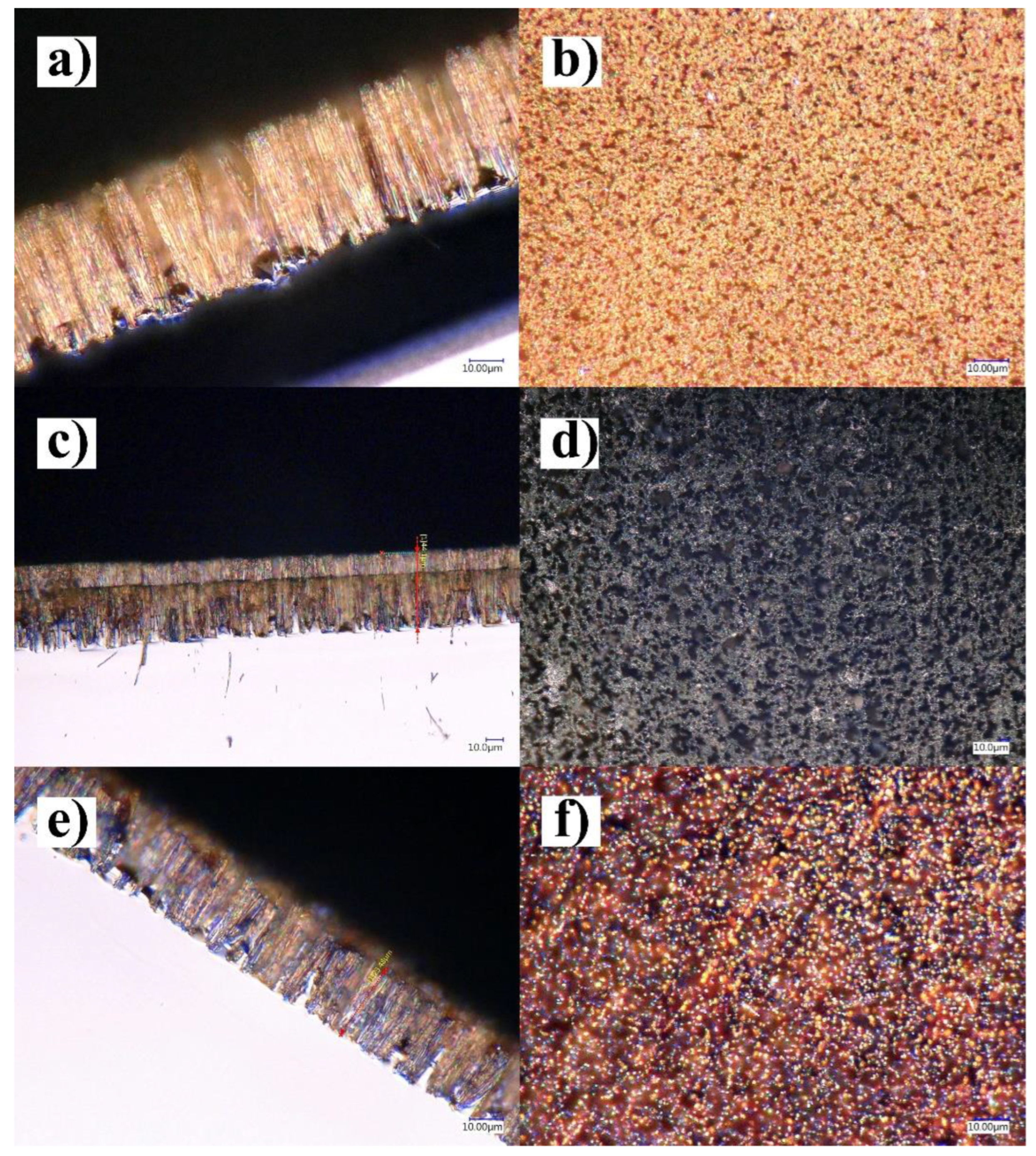
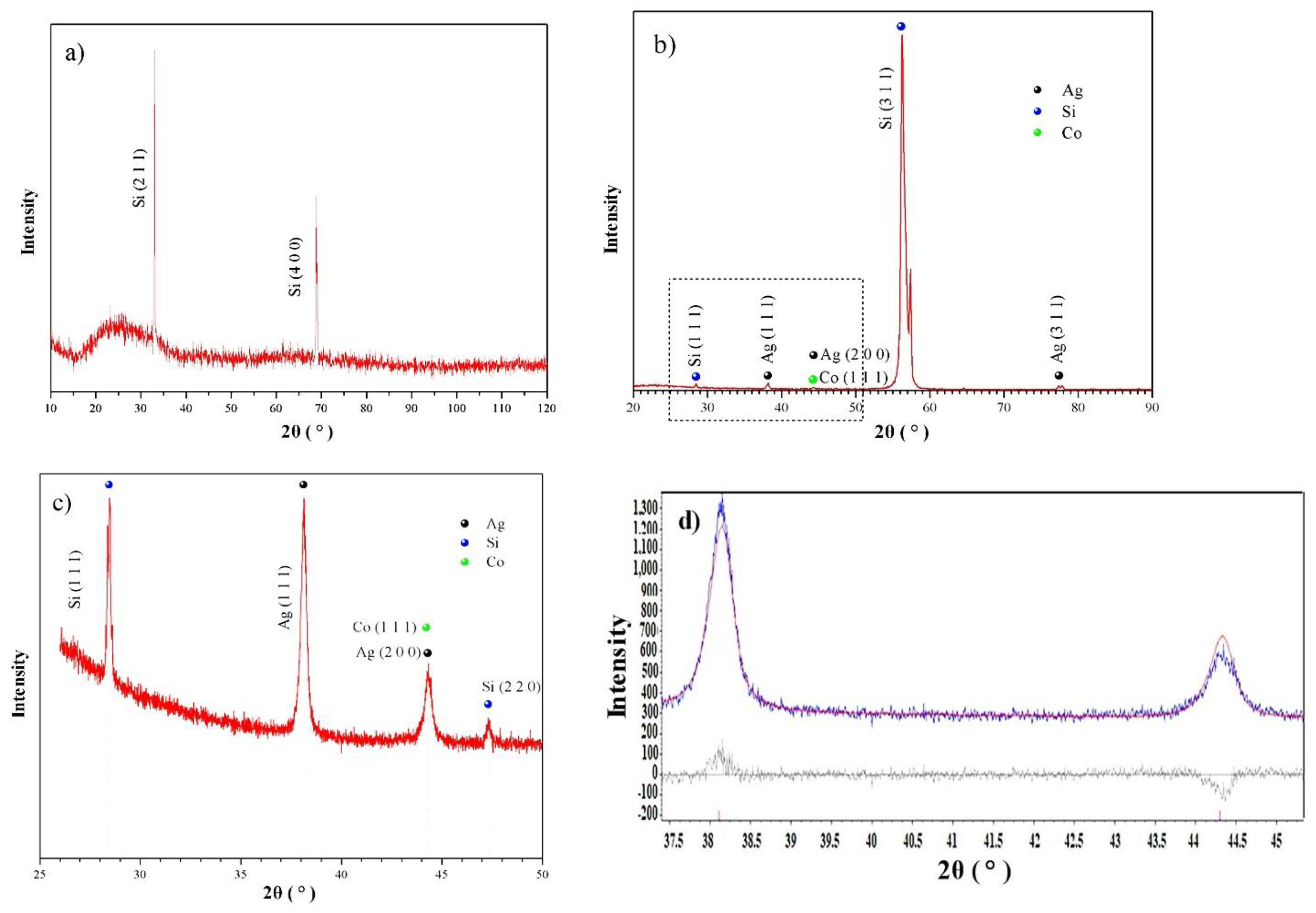
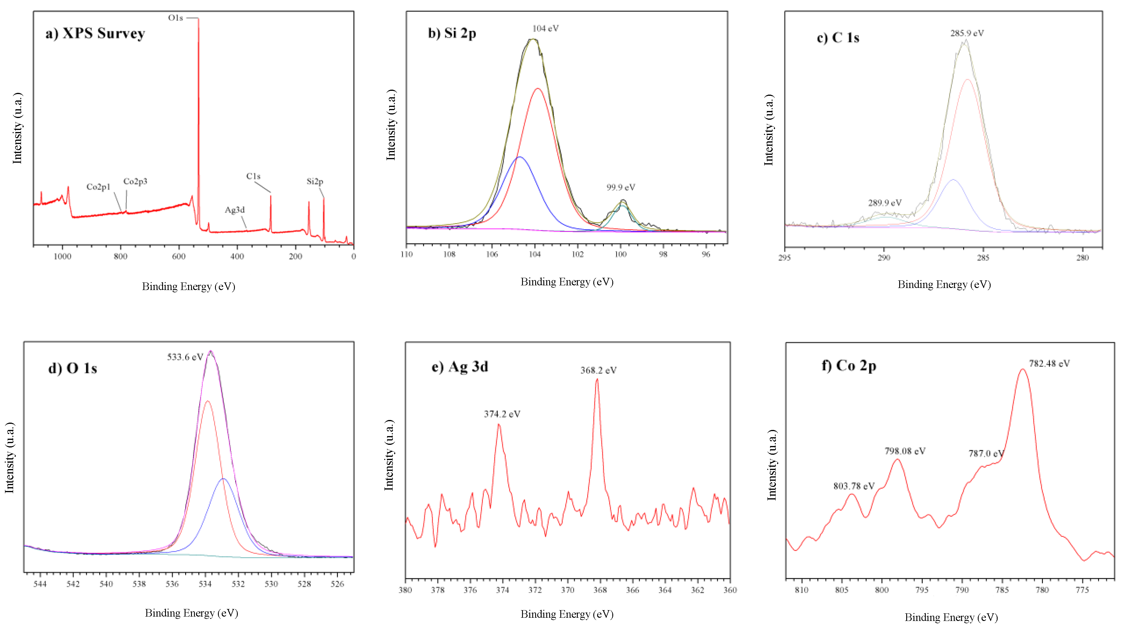
3.1. Characterization of the SiNWs-CuNPs and SiNWs-CoONPs

The topography and distribution of the synthesized nanowires were observed (Figure 4). In these visualizations, the central part of the silicon plates had a more homogeneous distribution of nanowires on the silicon plate. So, the micrographs of the differently prepared samples were taken in these areas. The explanation for observing the structure using optical or electronic microscopies is that those images show bundles or conglomerates of nanowires and only such groups are visible. The diameter of each nanowire only has slight fluctuations depending on the synthesis procedure (about 70–90 nm), different from their length which depends on many process variables (about 10–80 μm). Therefore, the MACE method indeed generates silicon nanowires.
Figure 4 shows the micrographs of SiNWs, SiNWs-CuNPs, and SiNWs-CoONPs. Figure 4a,b show the micrographs of a silicon nanowire plate (SiNWs). In Figure 4a, the SiNWs plate is seen in its cross-section, having an approximate length of 42.7 µm. Nanowires formed vertically on the silicon plate, which were abundant and not so far apart. Figure 4b shows the top view of the SiNWs plate. This micrograph shows the homogeneous distribution of the nanowires and the agglomerations that occur between them, forming small bundles. Figure 4c,d show the micrographs of a silicon nanowire plate decorated with copper nanoparticles (SiNWs-CuNPs). Figure 4c shows the cross-sectional view of the nanowires with a vertical orientation on the surface of the silicon plate and a length of about 44.1 µm.
Figure 4d shows the surface view of the SiNWs-CuNPs plate. There is a homogeneous distribution of nanowires and the islands formed by their agglomeration. Moreover, there is a color change on the surface due to the deposition of the copper nanoparticles. Figure 4e,f show the micrographs of a SiNWs plate decorated with cobalt nanoparticles (SiNWs-CoONPs). Figure 4e shows the cross-sectional view of this SiNWs -CoONPs plate. It should be noted that the formation of these nanowires occurred differently from the SiNWs shown in Figure 4a. In this case, the nanowires were formed vertically on the silicon surface but in a highly spaced distribution, having a length of about 23.48 µm. Figure 4f shows the superficial view, which shows the spacing between the nanowires (the bright points or areas correspond to nanowires). The micrograph has different color compared with that of the SiNWs and this is caused by the cobalt nanoparticles deposited on the nanowire surfaces.
In the optical images, there is the phenomenon of interference, observed as iridescent colors, because of the size of the filaments resulting from the MACE method and the space between them, which, as far as we know, this work is the first or between the few that show interference of visible light in the nanostructured bundles (Figure 4a,c,e,f), when observing them by Digital Optic Microscopy using 1000×–5000×. The rainbow-colored images resulted from the visible light of the microscope, causing interference when passing across the groups and between the nanowires according to the interference Equations (1) and (2) [54], maximum and minimum, respectively.
d = (   2   m   + 1   ) λ   4   n
d = m   λ 2   n
where, d is the optical thickness, n is the refractive index, λ is the wavelength, and m is an integer number (order of interference).
The silver, copper, and cobalt metallic particles were grown by the electroless method, which implies no use of an imposed external potential. Even more, no activation agents were used to seed the silicon surface and grow the metallic crystals. Therefore, the metallic ions were reduced both by the HF-treated silicon [17] and by electrons on the silicon surface, which were promoted from the valence band when absorbing light since the silicon had p-type doping and had no electrons in excess. The electroless method has a limited capability of increasing the mass of deposited metals beyond the nanometric scale (1–100 nm) because once the nucleation sites were covered, the potentials on these areas change and the active sites for further reductions diminish. Usually, the galvanic replacement reaction is followed by one or two electrolytic depositions to thicken the coatings. Consequently, the size of electroless grown metallic particles in about 10 s for silver, 5 s for cobalt, and 5 s for copper were nanometric in size [12,17,55].
Using scanning electron microscopy (SEM), the formation and structure of the synthesized silicon nanowires were observed in more detail. Moreover, the samples were analyzed using energy dispersive X-ray spectroscopy (EDS) to obtain the elemental mapping.
Figure 5 shows the SEM micrographs with a 10.00 µm scale bar and elemental point analysis on the cross-sectional area by EDS. Moreover, the figure shows the elemental mapping over the cross-sectional of the SiNWs-CoONPs sample. Figure 5a shows the SEM micrograph of the SiNWs sample at 1500×. In this secondary electron image, the length of the nanowires of about 32 µm is shown. Moreover, this image shows how the nanowires were agglomerated, forming small bundles. Some nanowires were broken, and some can have flections during the process of silicon etching. The concentration of H2O2 directly influences the morphology of the nanowires. On the other hand, Figure 5b, a micrograph made with backscattered electrons, gives a change in contrasts that allows observing the silver deposited at the base of the nanowires (bright white areas and dots). In some cases, the etching with HF, used to form nanowires, resulted in the silver nanoparticle agglomeration or dendritic forms. Part of the photocatalysis was attributed to these silver structures at the bottom of the nanowires. The silver–silicon junction, a Schottky barrier, is proposed as a higher efficient electron transferor when shaped as dendrites because the sharp shape has a lower work function, which means that it is easier to extract electrons from the pick than from a flat or round shape. In some other works, the silver or metal used to shape the structures is washed away with a nitric acid solution. Nonetheless, we agree with the works that propose that such a Schottky barrier contributes to photocatalysis.
EDS analysis was performed on the cross-sectional area of the SiNWs sample on the yellow rectangle of Figure 5a. The elements present were Si, C, O, and Ag in percentages of 80.14%, 12.71%, 3.96%, and 3.19%, respectively. C and O presence in the sample was attributed to the contamination when in contact with the atmosphere. Moreover, the oxygen present was related to the formation of oxides, in this case, with the Si. The samples of SiNWs-CuNPs were also characterized by SEM at 2000× and the micrographs are shown in Figure 5d,e. Figure 5d is an image of secondary electrons showing the nanowires with a length of about 48 µm. The nanowires were assembled into small bundles. Figure 5e was made with backscattered electrons showing contrasts between the silver deposited at the base of the nanowires in the form of dendrites (bright white areas) and the copper nanoparticles that decorate the tips of the nanowires (bright points). Figure 5f shows the elemental EDS analysis of SiNWs-CuNPs on the yellow rectangle area in Figure 5h. In this case, the elements present in the sample were Si, O, Cu, and Ag in a percentage of 83.27%, 11.41%, 3.28%, and 2.03%, respectively. The presence of copper in the sample indicates the deposition of copper nanoparticles on the nanowires. In this case, in addition to a SiO2 layer on top of the silicon, the oxygen can be attributed to a layer of copper oxides on top of the nanoparticles.
The 2200× SEM micrographs of the synthesized SiNWs-CoONPs are shown in Figure 5g,h. Figure 5g is an image generated by secondary electrons, where the length of the nanowires is about 30 µm. It is observed that the clusters of agglomerated nanowires at the bottom have a different thickness than at the top, so they end in a tip. On the other hand, Figure 5h shows the contrast of the silver in the form of dendrites (bright white areas in the SEM micrograph of backscattered electrons), that, after the formation of nanowires, remained in the bottom. These silver structures were not removed by washing with a nitric acid solution because they can contribute to photocatalysis.
In the reviewed literature, there were no reports of silver dendrites at the bottom of nanowires. In the elemental EDS analysis of the SiNWs-CoONPs (Figure 5i), corresponding to the area of the yellow rectangle of Figure 5h, the elements present in the sample were Si, O, C, Ag, Al, Na, and Co in a percentage of 62.59%, 20.25%, 14.27%, 1.30%, 1.12%, 0.41, and 0.06%, respectively. The presence of cobalt in the sample is an indicator of the deposition of cobalt on the nanowires, although its percentage is low due to the concentration of 0.01 M of CoCl2 in the electroless bath. However, the EDS analysis did not confirm the oxidation state of cobalt, identifying it as metallic or oxidized. The presences of Al and Na were because of residues generated in the SiNWs formation process. Na was part of the composition of the electroless bath and Al2O3 was an inlaid residue of the plate sanding. The distributions by zones of each element are shown in Figure 5j, where the elemental mapping of the SiNWs-CoONPs is shown.
The growth process of silver dendritic structures in the nanowire formation process was observed with SEM. Figure 6 shows the Ag dendritic structures observed on p-type monocrystalline silicon (c-Si) substrate immersed for 10 s into a mixture of HF (5M)/AgNO3 (0.035M) in an aqueous solution. Figure 6a shows a cross-sectional view of the surface composed of AgNPs and SiNWs. Figure 6b shows that the silicon substrate was covered with nanoparticles and dendrites of Ag. Moreover, this image gives evidence of a diversity of shapes of the crystalline dendrites and branches. The uniformity of a large number of such structures is illustrated in Figure 6c, showing that the products consist almost entirely of spike-shaped Ag dendrite crystals. Figure 6d shows the random orientation of the Ag crystals obtained by transforming the nanoparticles used initially for shaping the nanowires.
The Ag dendrite formation process is caused by the galvanic displacement reaction consisting of redox reactions that occur simultaneously on the silicon surface. The cathodic reaction reduces Ag+ on the Si wafer surface by injecting holes into the valence band of Si and generating Ag metallic particles. The anodic reaction results in the oxidation and dissolution of Si adjacent to Ag particles [56]. During the displacement reaction, the amorphous phase leads to rapid and continuous deposition on the surface of the growing particles, and several randomly oriented Ag particles spontaneously crystallizing from the amorphous phase. The Ag particles randomly oriented realign and grow in preferential directions, eventually forming single crystal dendrites. The growth rate, morphologies, and structures of Ag dendrites are highly dependent on Ag+ ion concentration (AgNO3), reaction time, and deposition temperature.
Figure 7a shows the diffractogram of the SiNWs surface. The diffractogram shows diffraction peaks at 33.038° and 69.13°, both peaks belong to the planes (2 1 1) and (4 0 0) of the Si (JCPS 01-072-1088 and JCPS 01-75-0589). The plane (4 0 0) of cubic silicon located at 69.13° of 2θ coincides with that reported by articles that use the same synthesis method [57]. Although, in this case, that peak is not the preferential direction since the 33.038° of 2θ peak corresponding to the Si plane (2 1 1) has a higher intensity. The change in the intensity of the peaks of silicon was attributed to the presence of the nanostructures. Moreover, there is a 25° peak associated with the presence of SiO2 generated by synthesizing the nanowires. The noise generated in the peak was due to the lack of a well-defined crystal structure.
Figure 7b shows the diffractogram of the surface of SiNWs-CoONPs performed in grazing-incidence diffraction mode with a tube position at 1°, in a range from 2° to 120° of 2θ, using a voltage and current of 40 kV and 40 mA, respectively. The diffractogram shows different diffraction peaks, the peaks at 28.44° and 56.12° belong to the planes (1 1 1) and (3 1 1) of the Si (JCPS 01-75-0589). The peaks at 38.12°, 44.3°, and 77.399° belong to the planes (1 1 1), (2 0 0), and (3 1 1) of the cubic Ag (JCPS 01-065-2871), respectively. The peak at 44.23° is associated with the plane (1 1 1) of the Co (JCPS 01-089-4307). Compared to the coupled mode diffractogram, the change in Si diffraction peaks can be observed on the surface of SiNWs-CoONPs. The preferential orientation of Si was in the plane (1 1 1) but the (3 1 1) shows an interference phenomenon [58,59] with the higher intensity occurring at 56.12° and not in the (2 1 1), as in the pattern of silicon powder. This interference can have possible additional peaks around the value of the central position. The appearance of the plane (1 1 1) was seen at 28.44°. There were probably slight alterations in the unit cells that the flexing of the SiNWs can cause. The stress caused by these flexes would make the unit cell smaller on one side and larger on the opposite.
Figure 7c was in grazing-incidence diffraction mode with a tube position at 4° 2θ, in a smaller range of 26° to 50° of 2θ. The higher resolution allows appreciating better the peaks already seen in Figure 7b. Moreover, it will enable observing the appearance of a new peak corresponding to the Si plane (2 2 0) at 47.305°. However, the plane (1 1 1) of the Co and the plane (2 0 0) of the Ag overlapped in the same peak. So, to determine if both elements were present, the Rietveld refinement was used (Figure 7d). By using the Rietveld refinement, the fitting was 100% with the Ag pattern and because the intensity of the peak in the adjustment (red line) was over that of the experimental diffractogram, it was not considered that Co (1 1 1) was present.
X-ray photoelectron spectroscopy (XPS) was used to determine the surface composition and oxidation states of a SiNWs-CoONPs sample. Figure 8a shows the complete XPS or survey spectrum and the identified elements were Si, C, O, Ag, and Co. In the Si2p signal (Figure 8b), two peaks were found at 99.9 eV and 104 eV corresponding to Si and SiO2, respectively. On the other hand, in the C1s, two signals were observed at 285.9 eV and 289.9 eV (Figure 8c). These signals are typical of adventitious carbon contamination, so carbon was not part of the sample. Figure 8d shows the O1s region with a single peak at 533.6 eV, corresponding to the CO bonds. It has a small shoulder at about 530.5 eV attributed to metal oxides, in this case, Co. Likewise, Figure 8e shows the Ag3d region having two signals at 368.2 eV and 374.2 Ev. These two peaks are within the range 378–366 eV that can be associated with metallic silver, while the strongest signal occurs at 368.2 eV and corresponds to the characteristic signal of metallic silver. Finally, in the Co2p region (Figure 8f), there are four peaks at 782.48 eV, 787.0 eV, 798.08 eV, and 803.78 eV. It can be noted that none of these peaks correspond to metallic Co, so all the deposited Co by electroless was oxidized in the process. The obtained spectrum in this sample can coincide with Co(OH)2 and CoO, but the difference between these signals is at most 1 eV, so the analysis was not conclusive, although it is very likely that both were present.
The reason for the Co deposit not being in its metallic form was attributed to the fact that during the synthesis process, the pH of the electroless solution was 14. The Pourbaix diagram of Co in aqueous solutions [34] indicates that Co2+ ions in an aqueous solution are below pH 9. At pH 14, there is a high concentration of OH ions forming Co(OH)2.

3.2. Heterogeneous Photocatalysis

For heterogeneous photocatalysis experiments, solutions having 20 ppm of MO, MB, and Rh6G were used as organic molecules for degradation. The photocatalysts used were SiNWs, SiNWs-CuNPs, and SiNWs-CoONPs. After photocatalysis, the collected samples were analyzed using a UV-Vis spectrophotometer, which showed the degradation of the MO and the chemisorption of MB and Rh6G.
Firstly, the dye calibration curves were experimentally obtained to know the changes made in the degradation of MO, MB, and Rh6G (Figure 9). Solutions with different concentrations were made and they were 2, 4, 6, 8, 10, 12, 14, 16, 18, and 20 ppm for each dye. Three different aliquots were taken for each solution. Then, the absorption spectra of the solutions were taken. From the obtained curves, the highest absorption peaks of the dyes were taken as reference points, which were 464 nm, 663 nm, and 526 nm for MO, MB, and Rh6G, respectively. In addition, an average was made with the maximum absorbance values of the three aliquots taken for each concentration that were plotted with the dye concentrations. Finally, a linear adjustment was made to the experimental data to generate the calibration curves of the three dyes, estimating the reduction in the concentration of the dyes after photocatalysis with SiNWs, SiNWs-CuNPs, and SiNWs-CoONPs.

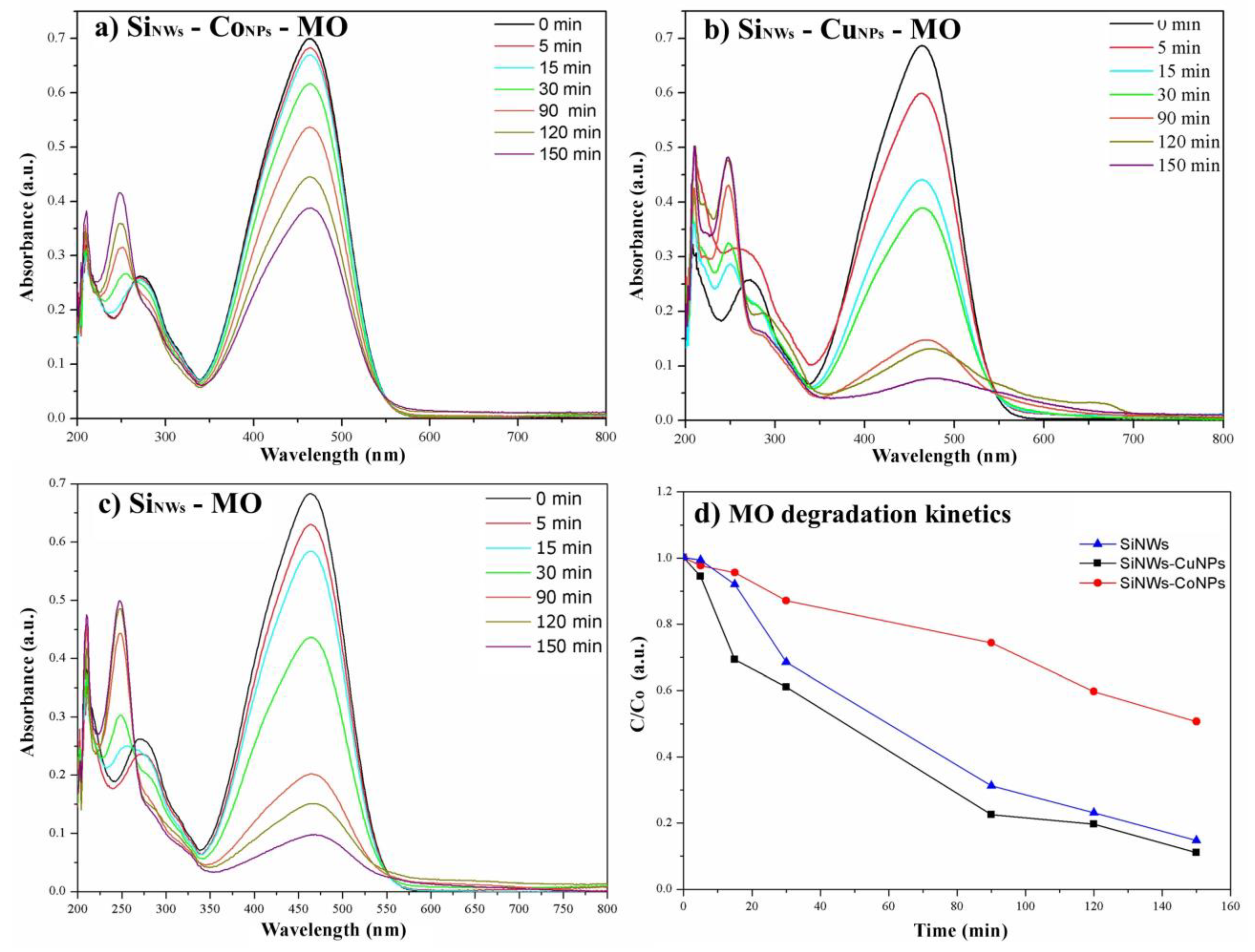
3.3. Photocatalysis with MO

Recurrently have been observed that SiNWs cause water splitting, which collaterally causes the pH reduction from 6.2, in the MO solution, to 4.3 on average. Figure 10 shows the photocatalytic activities of the SiNWs, SiNWs-CuNPs, and SiNWs-CoONPs with the MO using a white LED light. In this figure, the characteristic absorption peak of the MO at 464 nm decreases over time with the photocatalytic treatment, which is indicative of MO degradation. The maximum photocatalysis time was 150 min. This decrease in intensity occurs with the three photocatalysts (SiNWs, SiNWs-CuNPs, and SiNWs-CoONPs), suggesting a similar photocatalytic degradation process. However, it was observed that in the case of the SiNWs-CuNPs samples, the degradation of the MO was higher when reaching 150 min.
Figure 10d compares the photocatalytic activity with SiNWs and SiNWs-CoONPs have efficiencies at 150 min of 85.3% and 49.3%, respectively. The degradation efficiency of SiNWs-CuNPs ranges from 5.5% at 5 min to 88.9% at 150 min, which makes it the most efficient photocatalyst.
The degradation mechanisms of MO, MB, and Rh6G have been extensively investigated [27,28], which altogether with their other characteristics make them usual targets for testing catalysts.
In the spectra of Figure 10a, while the absorbance intensity decreases at 464 nm (λ corresponding to the azo bond), there was an increase in intensity at 448 nm (λ related to the amino group). This indicates a reduction in the concentration of the azo bonds, promoting the formation of the amino groups [60].
When comparing the efficiency of the three photocatalysts, the degradation kinetics of the SiNWs-CuNPs exhibit a behavior almost parallel to the SiNWs. However, the kinetics of SiNWs-CuNPs was slightly faster, having a rate constant (k) of about −0.14 compared with -0.012 of SiNWs, attributed to the contribution of Cu metallic nanoparticles deposited on their surface. Contrarily, when comparing SiNWs-CoONPs with SiNWs, there was a higher reduction in the rate of degradation kinetics. This was attributed to the CoO nanoparticles, which were not separating electron–hole pairs to contribute to the degradation of the organic molecule of the MO. Table 1 shows that all the reactions in this study were of order 1 for the three semiconductor systems with each of the three dyes.

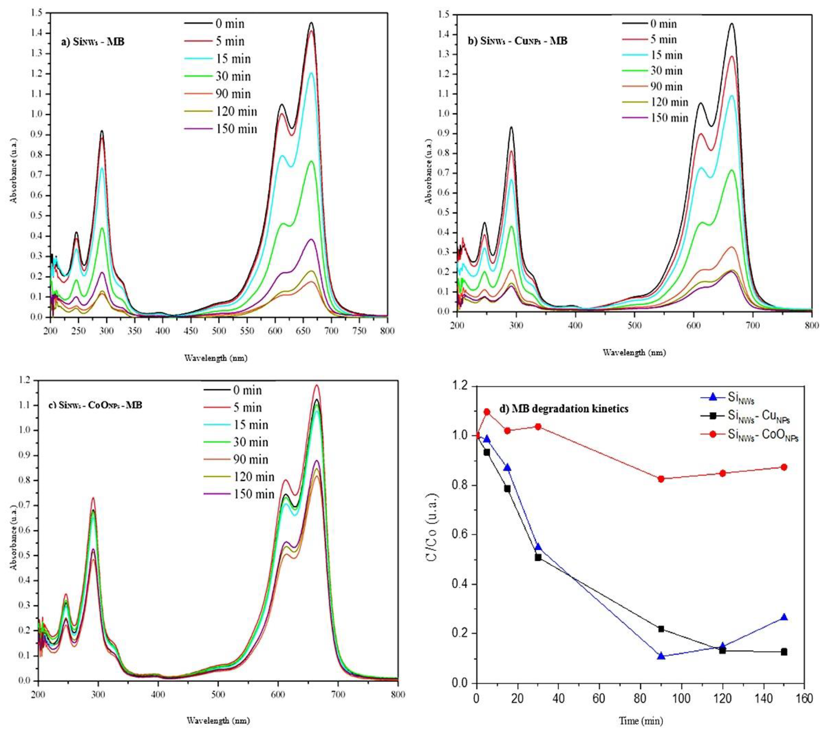
3.4. Photocatalysis with MB

Figure 11 shows the photocatalytic activity in the MB of the SiNWs, SiNWs-CuNPs, and SiNWs-CoONPs with LED light. In this figure, the MB chemisorption was observed as the intensity decreases at its characteristic absorption peak, at 663 nm. However, the intensity of that peak does not decrease over time. Similar to the UV-Vis spectrum of SiNWs, the intensity of the peak increases after 90 min instead of decreasing. The same happened at different times in the absorption spectrum of SiNWs-CoONPs.
Brik et al. [61], using silicon nanowires for MB degradation, found a 21% reduction attributed to molecule absorption on the surface. They show significant changes in the degradation percentages even using a UV source. Ameen et al. [62] attribute the dye reduction in the dark, using SiNWs as a photocatalyst, to the retention of the molecules by the large surface area of the nanowires.
Figure 11d compares the photocatalytic activities of the three photocatalysts. The highest chemisorption efficiency of SiNWs-CuNPs was 87.2% at 150 min. This was the only photocatalyst with different behavior. The highest chemisorption efficiency of SiNWs was 86% at minute 90 because, by minute 50, their efficiency decreased to 73%. In the case of the SiNWs-CoONPs photocatalyst, its maximum chemisorption efficiency was 17.3% at minute 90 and by the end of the period, its efficiency decreased to 12.6%.
The UV-Vis absorption spectra of the photocatalysts show that the peak at 663 nm decreased and that there were no new peaks. So, in the case of MB, it was attributed that the phenomenon was not the degradation but the adsorption of organic molecules [60]. Moreover, the desorption of the molecules was shown, which explains why the absorbance increases at certain times of photocatalysis [16]. This process was identified as chemisorption and that behavior was attributed to a combination of absorption/desorption regulated by the changing parameters of the solution. The absence of degradation of the organic molecules was attributed to the lack of the potential necessary to break the bonds of that molecule with three aromatic rings. As with MO, the highest decoloration was obtained with that of SiNWs-CuNPs, followed by SiNWs, and SiNWs-CoONPs as the lowest.

3.5. Photocatalysis with Rh6G

Figure 12 shows the photocatalytic activity in the Rh6G with the SiNWs, SiNWs-CoONPs, and SiNWs-CuNPs with LED light. The Rh6G has its characteristic absorption peak at 526 nm, so as the intensity at that peak decreases with increasing photocatalysis time, dye chemisorption occurs as in the SiNWs-CuNPs spectrum. However, in the SiNWs and SiNWs-CoONPs spectra, this peak intensity does not decrease over time.
Figure 12d compares the photocatalytic activities of the three photocatalysts. In this way, the SiNWs-CuNPs had a chemisorption efficiency of 86.88% at 150 min, while the highest chemisorption efficiency of the SiNWs was 87% at 120 min. In the case of the SiNWs-CoONPs photocatalyst, its maximum chemisorption efficiency was approximately 12% at minute 5.
On the other hand, the UV-Vis absorption spectra of the photocatalysts show that as the peak decreases at 526 nm, there was no creation of new peaks, so it was attributed that the phenomenon present in Rh6G photocatalysis was not degradation, but the adsorption of organic molecules similarly to MB [60]. Again, similarly to MB, the desorption of the molecules was observed, explaining the increases at certain times of the photocatalysis [16]. The degradation of the Rh6G organic molecule was not achieved due to the lack of potential in the photocatalysts linked to the ability to concentrate charges by the resistivity of the semiconductor. The molecular structure of Rh6G has multiple aromatic rings, which need a sufficient amount of energy to break their bonds.
As with MB, the adsorption and desorption of organic dye molecules occurred, with the most efficient photocatalyst being SiNWs-CuNPs. In the case of SiNWs and SiNWs-CoONPs exhibiting dye desorption, there was a reduction in chemisorption efficiency, which was very large in SiNWs-CoNPs because the deposited Co nanoparticles probably were oxidized and could be as Co(OH)2/CoO deposited on the surface. It should be noted that the difference in efficiency between SiNWs and SiNWs-CoONPs was minimal.
The reason for the desorption of the dye molecules was attributed to the fact that, in the cathodic regions present on the surface of the nanowires, where there was a considerable accumulation of electrons (negative charge), molecular adsorption was carried out preferably until saturation. However, when these regions lose their charge (electric discharge), the process of desorption occurs because the charge of the molecule was no longer related to the charge on the surface of the nanowires.

3.6. Review and Comparison of Photodegradations of MO, MB, and Rh B Dyes by SiNWs

Table 2 shows a brief review of the literature that use SiNWs as photocatalysts with different crystalline orientation, heterojunction with other semiconductors, light sources, target dye molecule, dye concentration in aqueous solutions, treatment time, and degradation efficiencies.
The three dyes (MO, MB, and Rh 6G) have been used as target molecules to evaluate many different photocatalysts. In the case of SiNWs, this table resumes some process parameters but many more cause differences in the degradation efficiencies. Moreover, there is a growing tendency to use heterojunctions with other semiconductors in addition to the variations of metallic decorating nanoparticles. In some cases, there is missing information about these or other parameters, such as the power of illumination, the heating of the aqueous solution, the atmospheric pressure, pulsed illumination, potential in case of photoelectrocatalysis, volume of the samples, area of lighting, and so forth.
The MO degradation kinetics were in the sequence SiNWs-CuNPs (88.9%) > SiNWs (85.3%) > SiNWs-CoONPs (49.3%), with the SiNWs-CuNPs having slightly faster kinetics. However, SiNWs-CoONPs have slow degradation kinetics. In the references of Table 2, there are some of them with higher efficiencies than in this work, included in the last rows, especially using CuNPs. The proposal in this work points to CoO as a more stable photocatalyst than CuO2. This does not imply that it has higher degradation efficiencies, which are lower in the conditions tested here. One of the reasons for such results was a lower obtained deposited amount of CoO. According with the EDS quantifications, SiNWs (Ag 3.98%), SiNWs-CuNPs (Ag 2.43%, Cu 3.94%), SiNWs-CoONPs (Ag 2.01%, Co 0.01%), normalizing relative to the silicon content. The deposited nanoparticles, including Cu and Co, were by electroless without adding an activator, which means that the nanowires own potentials and electron supply regulates, in part, the kinetics and amount of depositions.
In the case of working with oxides, CuO2 and CoO, they should not require further processing to maintain stability on multiple runs. Nonetheless, all the known reports show decrements in consecutive tests even considering that the solutions have neither other pollutants nor salts. This is another main reason, together with electron–hole recombinations, for photocatalysis has not been used broadly. One explanation for this is that this process is based on redox reactions, which generate ionic compounds as byproducts. Such charged species increase the double layer around the active sites having cathodic or anodic potentials, which blocks them, in part, causing diminish in efficiencies.

4. Conclusions

The SiNWs were synthesized using the MACE method. The SiNWs-CuNPs were synthesized by depositing the Cu nanoparticles auto-catalytically. Similarly, the SiNWs-CoONPs were synthesized firstly as Co and oxidized in the same process. The nanowires had a length of about 23 µm to 30 µm with a vertical structure on the wafer. They were peak-shaped and spaced.
Silicon wafers have no photocatalytic effect lacking the potential for splitting water or causing redox reactions. SiNWS, without Schottky barriers or further doping, have a higher area but keep the silicon characteristics. SiNWs, SiNWs-CoONPs, and SiNWs-CuNPs, prepared in the described procedure and having Ag at the bottom, manifest the effects shown in this and other works. There were dendritic conformations of the silver nanoparticles at the bottom, originally used for generating the nanowire bundles. This structure type can contribute to faster electron transfer.
In the optical images, there is the phenomenon of interference, observed as iridescent colors, because of the size of the filaments resulting from the MACE method and the space between them, which, as far as we know, this work is the first or between the few that show interference of visible light in the nanostructured bundles. Moreover, there was interference in the plane (3 1 1) for the X-ray diffractograms caused by the coincidence of the Cukα1 (1.5604 Å) under grazing incidence with the silicon plane distance.
The EDS analysis confirmed the presence of Co in the samples (oxidized). In the case of SiNWs-CuNPs, the approximate length of the nanowires was between 44 µm and 48 µm. They showed a vertical structure on the plate, homogeneity, and agglomerations between nanowires. The EDS analysis confirmed the presence of Cu.
The XPS analyses on the SiNWs-CoONPs samples show that the deposited of Co was not in metallic form but as CoONPs or as Co(OH)2/CoO. The pH bath conditions allowed obtaining CoONPs instead of metallic cobalt.
In the case of MO, the degradation kinetics of SiNWs-Cu and SiNWs were almost parallel, with SiNWs-CuNPs having slightly faster kinetics due to the contribution of Cu in photocatalysis. SiNWs-CoONPs were found to have very slow degradation kinetics. This was attributed to the cobalt oxide that, contrary to Cu nanoparticles, did not contribute to the electron–hole separation.
MB and Rh6G showed no degradation of the dye molecules during the tests; instead, there was adsorption and desorption of them. The most efficient photocatalyst was SiNWs-CuNPs. Nonetheless, it should be noted that SiNWs and SiNWs-CuNPs show similar efficiencies. SiNWs-CoONPs show substantially less efficiency.
The photocatalytic activity of this work’s materials, the SiNWs, SiNWs-CuNPs, and SiNWs-CoONPs, depend not only on the materials themselves but also on multiple factors, which alter the kinetics and final efficiencies. Under the conditions reported, with the characteristics described, all the materials were photocatalytic, but in the sequence SiNWs-CuNPs > SiNWs > SiNWs-CoONPs. Even more, their capability of degrading methyl orange was not replicated for methylene blue and rhodamine 6G, which shows that, in addition to the factors to that sequence, there are others to address when changing the target for decomposing. The tests can be repeated several times, but there is a decrement caused by sorption on the surfaces of ionic byproducts of the decomposition, changes in the oxidation state of CuNPs, chemical reactions, and various other processes.

Author Contributions

Conceptualization, J.d.J.P.B.; methodology O.A.C.C., J.d.J.P.B., Y.C.M., C.H.R., A.X.M.P. and M.R.G.R.; validation, O.A.C.C., J.d.J.P.B. and D.C.A.; formal analysis, O.A.C.C. and J.d.J.P.B.; investigation, O.A.C.C., J.d.J.P.B. and M.R.G.R.; resources, O.A.C.C., J.d.J.P.B., Y.C.M., C.H.R., C.M.L., M.R.G.R., J.G.F.L. and H.R.S.; data curation, O.A.C.C., J.d.J.P.B., C.M.L., J.G.F.L. and H.R.S.; writing—original draft preparation, O.A.C.C., J.d.J.P.B. and D.C.A.; writing—review and editing, J.d.J.P.B., C.H.R., A.X.M.P., M.L.M.L. and G.O.; visualization, O.A.C.C., J.d.J.P.B. and A.X.M.P.; supervision, J.d.J.P.B. and D.C.A.; project administration, J.d.J.P.B. and M.L.M.L.; funding acquisition, J.d.J.P.B. and M.L.M.L. All authors have read and agreed to the published version of the manuscript.

Funding

This research was funded by “Fondo Sectorial CONACYT-SENER Sustentabilidad Energética” through Grant 207450, “Centro Mexicano de Innovación en Energía Solar (CeMIESol)”, within strategic project No. P62, “Prototype hybrid system of a supercritical CO2 expander with flat polycarbonate mirrors on automated heliostats”. This work was supported by the National Council of Science and Technology CONACYT (México), through the Basic and/or Frontier Science grant No. 320114, the National Laboratory of Graphenic Materials, and the LANIAUTO.

Informed Consent Statement

Not applicable.

Acknowledgments

The authors thank the CIDETEQ’s staff members who supported the processes necessary to carry out the projects and laboratory activities.

Conflicts of Interest

The authors declare no conflict of interest.

References

  1. Abebe, B.; Ananda Murthy, H.C.; Dessie, Y. Synthesis and Characterization of Ti–Fe Oxide Nanomaterials: Adsorption–Degradation of Methyl Orange Dye. Arab. J. Sci. Eng. 2020, 45, 4609–4620. [Google Scholar] [CrossRef]
  2. Shen, Y.; Zhang, Z.; Xiao, K. Evaluation of Cobalt Oxide, Copper Oxide and Their Solid Solutions as Heterogeneous Catalysts for Fenton-Degradation of Dye Pollutants. RSC Adv. 2015, 5, 91846–91854. [Google Scholar] [CrossRef]
  3. Salierno, G.; Napoleone, S.; Maisterrena, A.; Cassanello, M.; Pellasio, M.; Doumic, L.; Ayude, M.A. Continuous Heterogeneous Fenton-Type Process for Dye Pollution Abatement Intensified by Hydrodynamic Cavitation. Ind. Eng. Chem. Res 2021, 60, 16653–16664. [Google Scholar] [CrossRef]
  4. Rizzo, L.; Malato, S.; Antakyali, D.; Beretsou, V.G.; Đolić, M.B.; Gernjak, W.; Heath, E.; Ivancev-Tumbas, I.; Karaolia, P.; Lado Ribeiro, A.R.; et al. Consolidated vs New Advanced Treatment Methods for the Removal of Contaminants of Emerging Concern from Urban Wastewater. Sci. Total Environ. 2019, 655, 986–1008. [Google Scholar] [CrossRef]
  5. Johnston, A.L.; Lester, E.; Williams, O.; Gomes, R.L. Understanding Layered Double Hydroxide Properties as Sorbent Materials for Removing Organic Pollutants from Environmental Waters. J. Environ. Chem. Eng. 2021, 9, 105197. [Google Scholar] [CrossRef]
  6. Li, C.; Li, J.; Wang, N.; Zhao, Q.; Wang, P. Status of the Treatment of Produced Water Containing Polymer in Oilfields: A Review. J. Environ. Chem. Eng. 2021, 9, 105303. [Google Scholar] [CrossRef]
  7. Hernández-Morales, V.; Nava, R.; Acosta-Silva, Y.J.; MacÍas-Sánchez, S.A.; Pérez-Bueno, J.J.; Pawelec, B. Adsorption of Lead (II) on SBA-15 Mesoporous Molecular Sieve Functionalized with −NH2 Groups. Microporous Mesoporous Mater. 2012, 160, 133–142. [Google Scholar] [CrossRef]
  8. Martínez, M.G.A.; de Jesus Pérez-Bueno, J.; Reza, E.M.; López, M.L.M. Lead Adsorption in Manganese Oxides as Powders and Coatings Supported on Silica Gel Beads and Tin Inverse Opal-Like Structures. Curr. Anal. Chem. 2020, 17, 831–838. [Google Scholar] [CrossRef]
  9. Faucher, S.; Aluru, N.; Bazant, M.Z.; Blankschtein, D.; Brozena, A.H.; Cumings, J.; Pedro De Souza, J.; Elimelech, M.; Epsztein, R.; Fourkas, J.T.; et al. Critical Knowledge Gaps in Mass Transport through Single-Digit Nanopores: A Review and Perspective. J. Phys. Chem. C 2019, 123, 21309–21326. [Google Scholar] [CrossRef]
  10. Márquez, E.E.; Zarazúa, G.M.S.; Bueno, J.D.J.P. Prospects for the Use of Electrooxidation and Electrocoagulation Techniques for Membrane Filtration of Irrigation Water. Environ. Process. 2020, 7, 391–420. [Google Scholar] [CrossRef]
  11. Olea, M.A.U.; Bueno, J.D.J.P.; Pérez, A.X.M. Nanometric and Surface Properties of Semiconductors Correlated to Photocatalysis and Photoelectrocatalysis Applied to Organic Pollutants—A Review. J. Environ. Chem. Eng. 2021, 9, 106480. [Google Scholar] [CrossRef]
  12. Robles, M.R.G.; Bueno, J.D.J.P.; Syllas, C.S.A.; López, M.L.M.; Guerrero, F.M. Silver/Silicon Nanowires/Copper Nanoparticles Heterojunction for Methyl Orange Degradation by Heterogeneous Photocatalysis under Visible Irradiation. MRS Adv. 2018, 3, 3933–3938. [Google Scholar] [CrossRef]
  13. Magallón-Cacho, L.; Pérez-Bueno, J.J.; Meas-Vong, Y.; Stremsdoerfer, G.; Espinoza-Beltrán, F.J. Surface Modification of Acrylonitrile-Butadiene-Styrene (ABS) with Heterogeneous Photocatalysis (TiO2) for the Substitution of the Etching Stage in the Electroless Process. Surf. Coat. Technol. 2011, 206, 1410–1415. [Google Scholar] [CrossRef]
  14. Garcia, E.M.; Santos, J.S.; Pereira, E.C.; Freitas, M.B.J.G. Electrodeposition of Cobalt from Spent Li-Ion Battery Cathodes by the Electrochemistry Quartz Crystal Microbalance Technique. J. Power Sources 2008, 185, 549–553. [Google Scholar] [CrossRef]
  15. Zeferino, R.S.; Pal, U.; De Anda Reues, M.E.; Rosas, E.R. Indium Doping Induced Defect Structure Evolution and Photocatalytic Activity of Hydrothermally Grown Small SnO2 Nanoparticles. Adv. Nano Res. 2019, 7, 13–24. [Google Scholar] [CrossRef]
  16. De Lourdes Ruiz Peralta, M.; Sánchez-Cantú, M.; Puente-López, E.; Rubio-Rosas, E.; Tzompantzi, F. Evaluation of Calcium Oxide in Rhodamine 6G Photodegradation. Catal. Today 2018, 305, 75–81. [Google Scholar] [CrossRef]
  17. Amdouni, S.; Cherifi, Y.; Coffinier, Y.; Addad, A.; Zaïbi, M.A.; Oueslati, M.; Boukherroub, R.; Zaibie, M.A.; Oueslati, M.; Boukherroub, R. Gold Nanoparticles Coated Silicon Nanowires for Efficient Catalytic and Photocatalytic Applications. Mater. Sci. Semicond. Process. 2018, 75, 206–213. [Google Scholar] [CrossRef]
  18. Brahiti, N.; Hadjersi, T.; Amirouche, S.; Menari, H.; ElKechai, O. Photocatalytic Degradation of Cationic and Anionic Dyes in Water Using Hydrogen-Terminated Silicon Nanowires as Catalyst. Int. J. Hydrog. Energy 2018, 43, 11411–11421. [Google Scholar] [CrossRef]
  19. Hamdi, A.; Boussekey, L.; Roussel, P.; Addad, A.; Ezzaouia, H.; Boukherroub, R.; Coffinier, Y. Hydrothermal Preparation of MoS2/TiO2/Si Nanowires Composite with Enhanced Photocatalytic Performance under Visible Light. Mater. Des. 2016, 109, 634–643. [Google Scholar] [CrossRef]
  20. Ifires, M.; Hadjersi, T.; Chegroune, R.; Lamrani, S.; Moulai, F.; Mebarki, M.; Manseri, A. One-Step Electrodeposition of Superhydrophobic NiO-Co(OH)2 Urchin-like Structures on Si Nanowires as Photocatalyst for RhB Degradation under Visible Light. J. Alloys Compd. 2019, 774, 908–917. [Google Scholar] [CrossRef]
  21. Busra, U.; Omer, C. Free Vibration Analysis Silicon Nanowires Surrounded by Elastic Matrix by Nonlocal Finite Element Method. Adv. Nano Res. 2019, 7, 99–108. [Google Scholar] [CrossRef]
  22. Arciga-Duran, E.; Meas, Y.; Pérez-Bueno, J.J.; Ballesteros, J.C.; Trejo, G. Electrochemical Synthesis of Co3O4−x Films for Their Application as Oxygen Evolution Reaction Electrocatalysts: Role of Oxygen Vacancies. J. Electrochem. Soc. 2018, 165, H3178–H3186. [Google Scholar] [CrossRef]
  23. Lu, K.-Q.Q.; Lin, X.; Tang, Z.-R.R.; Xu, Y.-J.J. Silicon Nanowires@Co3O4 Arrays Film with Z-scheme Band Alignment for Hydrogen Evolution. Catal. Today 2019, 335, 294–299. [Google Scholar] [CrossRef]
  24. Yang, R.Q.; Ji, Y.C.; Li, Q.; Zhao, Z.H.; Zhang, R.T.; Liang, L.L.; Liu, F.; Chen, Y.K.; Han, S.W.; Yu, X.; et al. Ultrafine Si Nanowires/Sn3O4 Nanosheets 3D Hierarchical Heterostructured Array as a Photoanode with High-Efficient Photoelectrocatalytic Performance. Appl. Catal. B Environ. 2019, 256, 117798. [Google Scholar] [CrossRef]
  25. Ghosh, P.; Kar, A.; Khandelwal, S.; Vyas, D.; Mir, A.Q.; Chakraborty, A.L.; Hegde, R.S.; Sharma, S.; Dutta, A.; Khatua, S. Plasmonic CoO-Decorated Au Nanorods for Photoelectrocatalytic Water Oxidation. ACS Appl. Nano Mater. 2019, 2, 5795–5803. [Google Scholar] [CrossRef]
  26. Brieño-Enriquez, K.M.; Ledesma-García, J.; Perez-Bueno, J.J.; Godinez, L.A.; Terrones, H.; Ángeles-Chavez, C. Bonding Titanium on Multi-Walled Carbon Nanotubes for Hydrogen Storage: An Electrochemical Approach. Mater. Chem. Phys. 2009, 115, 521–525. [Google Scholar] [CrossRef]
  27. Ildefonso, Z.T.; José de Jesús, P.B.; Celeste Yunueth, T.L.; Luis, L.R.; Maria Luisa, M.L.; Yunny, M.V. A Phenomenon of Degradation of Methyl Orange Observed during the Reaction of NH4TiOF3 Nanotubes with the Aqueous Medium to Produce TiO2 Anatase Nanoparticles. RSC Adv. 2016, 6, 76167–76173. [Google Scholar] [CrossRef]
  28. Torres, I.Z.; Bueno, J.D.J.P.; López, C.Y.T.; Rojas, L.L.; López, M.L.M.; Vong, Y.M. Nanotubes with Anatase Nanoparticulate Walls Obtained from NH4TiOF3 Nanotubes Prepared by Anodizing Ti. RSC Adv. 2016, 6, 41637–41643. [Google Scholar] [CrossRef]
  29. Chen, Y.J.; Zhu, P.F.; Duan, M.; Li, J.; Ren, Z.H.; Wang, P.P. Fabrication of a Magnetically Separable and Dual Z-Scheme PANI/Ag3PO4/NiFe2O4 Composite with Enhanced Visible-Light Photocatalytic Activity for Organic Pollutant Elimination. Appl. Surf. Sci. 2019, 486, 198–211. [Google Scholar] [CrossRef]
  30. Zhu, Y.; Zhang, T.; An, T.; Zong, Y.; Lee, J.Y. Unraveling the Electrocatalytically Active Sites and Stability of Co & Co Oxides on Nanocarbon for Oxygen Evolution Reaction in Acid Solution. J. Energy Chem. 2020, 49, 8–13. [Google Scholar] [CrossRef]
  31. Sun, T.; Liu, P.; Zhang, Y.; Chen, Z.; Zhang, C.; Guo, X.; Ma, C.; Gao, Y.; Zhang, S. Boosting the Electrochemical Water Splitting on Co3O4 through Surface Decoration of Epitaxial S-Doped CoO Layers. Chem. Eng. J. 2020, 390, 124591. [Google Scholar] [CrossRef]
  32. Shi, W.; Guo, F.; Li, M.; Shi, Y.; Shi, M.; Yan, C. Constructing 3D Sub-Micrometer CoO Octahedrons Packed with Layered MoS2 Shell for Boosting Photocatalytic Overall Water Splitting Activity. Appl. Surf. Sci. 2019, 473, 928–933. [Google Scholar] [CrossRef]
  33. Zhu, S.; Liao, W.; Zhang, M.; Liang, S. Design of Spatially Separated Au and CoO Dual Cocatalysts on Hollow TiO2 for Enhanced Photocatalytic Activity towards the Reduction of CO2 to CH4. Chem. Eng. J. 2019, 361, 461–469. [Google Scholar] [CrossRef]
  34. Boughelout, A.; Macaluso, R.; Kechouane, M.; Trari, M. Photocatalysis of Rhodamine B and Methyl Orange Degradation under Solar Light on ZnO and Cu2O Thin Films. React. Kinet. Mech. Catal. 2020, 129, 1115–1130. [Google Scholar] [CrossRef]
  35. Rasheed, P.; Haq, S.; Waseem, M.; Rehman, S.U.; Rehman, W.; Bibi, N.; Shah, S.A.A. Green Synthesis of Vanadium Oxide-Zirconium Oxide Nanocomposite for the Degradation of Methyl Orange and Picloram. Mater. Res. Express 2020, 7, 025011. [Google Scholar] [CrossRef]
  36. Han, Y.-Q.; Lei, L.; Yang, C.; Zhang, S.-Y.; Zhao, Q.; Zhang, X.-J. Mechanism underlying photocatalyzed degradation of methyl orange by layered black phosphorus. J. Appl. Ecol. 2020, 31, 333–339. [Google Scholar] [CrossRef]
  37. Khatri, A.; Rana, P.S. Visible Light Assisted Photocatalysis of Methylene Blue and Rose Bengal Dyes by Iron Doped NiO Nanoparticles Prepared via Chemical Co-Precipitation. Phys. B Condens. Matter 2020, 579, 411905. [Google Scholar] [CrossRef]
  38. Sa-Nguanprang, S.; Phuruangrat, A.; Thongtem, T.; Thongtem, S. Preparation of Visible-Light-Driven Al-Doped ZnO Nanoparticles Used for Photodegradation of Methylene Blue. J. Electron. Mater. 2020, 49, 1841–1848. [Google Scholar] [CrossRef]
  39. Varnagiris, S.; Urbonavicius, M.; Sakalauskaite, S.; Daugelavicius, R.; Pranevicius, L.; Lelis, M.; Milcius, D. Floating TiO2 Photocatalyst for Efficient Inactivation of E. Coli and Decomposition of Methylene Blue Solution. Sci. Total Environ. 2020, 720, 137600. [Google Scholar] [CrossRef]
  40. Haimerl, J.M.; Ghosh, I.; König, B.; Lupton, J.M.; Vogelsang, J. Chemical Photocatalysis with Rhodamine 6G: Investigation of Photoreduction by Simultaneous Fluorescence Correlation Spectroscopy and Fluorescence Lifetime Measurements. J. Phys. Chem. B 2018, 122, 10728–10735. [Google Scholar] [CrossRef]
  41. Tang, C.; Chen, C.; Zhang, H.; Zhang, J.; Li, Z. Enhancement of Degradation for Nitrogen Doped Zinc Oxide to Degrade Methylene Blue. Phys. B Condens. Matter 2020, 583, 412029. [Google Scholar] [CrossRef]
  42. Van de Linde, S.; Sauer, M. How to Switch a Fluorophore: From Undesired Blinking to Controlled Photoswitching. Chem. Soc. Rev. 2014, 43, 1076–1087. [Google Scholar] [CrossRef] [PubMed]
  43. Pérez-Bueno, J.J.; Vasquez-García, S.R.; García-González, L.; Vorobiev, Y.V.; Luna-Bárcenas, G.; González-Hernández, J. Optical Processes in PMMA, SiO2, and Hybrid Organic-Inorganic Sol-Gel Films Colored with Rhodamine 6GDN. J. Phys. Chem. B 2002, 106, 1550–1556. [Google Scholar] [CrossRef]
  44. Mirzaei, A.; Kang, S.Y.; Choi, S.W.; Kwon, Y.J.; Choi, M.S.; Bang, J.H.; Kim, S.S.; Kim, H.W. Fabrication and Gas Sensing Properties of Vertically Aligned Si Nanowires. Appl. Surf. Sci. 2018, 427, 215–226. [Google Scholar] [CrossRef]
  45. Martínez-Hernández, A.; Méndez-Albores, A.; Arciga-Duran, E.; Flores, J.G.; Pérez-Bueno, J.J.; Meas, Y.; Trejo, G. Effect of Heat Treatment on the Hardness and Wear Resistance of Electrodeposited Co-B Alloy Coatings. J. Mater. Res. Technol. 2019, 8, 960–968. [Google Scholar] [CrossRef]
  46. Huang, Z.; Geyer, N.; Werner, P.; De Boor, J.; Gösele, U. Metal-Assisted Chemical Etching of Silicon: A Review. Adv. Mater 2011, 23, 285–308. [Google Scholar] [CrossRef]
  47. Franz, M.; Junghans, R.; Schmitt, P.; Szeghalmi, A.; Schulz, S.E. Wafer-Level Integration of Self-Aligned High Aspect Ratio Silicon 3D Structures Using the MACE Method with Au, Pd, Pt, Cu, and Ir. Beilstein J. Nanotechnol. 2020, 11, 1439–1449. [Google Scholar] [CrossRef]
  48. Le Nguyen, N.; Phan, T.C.H.; Dang, T.M.D.; Dang, M.C. Formation of Silver Nanoparticles and Their Application for Suppressing Surface Reflection of N-Type Silicon. Adv. Nat. Sci. Nanosci. Nanotechnol. 2019, 10, 025014. [Google Scholar] [CrossRef]
  49. Leonardi, A.; Faro, M.; Irrera, A. Silicon Nanowires Synthesis by Metal-Assisted Chemical Etching: A Review. Nanomaterials 2021, 11, 383. [Google Scholar] [CrossRef]
  50. Canevali, C.; Alia, M.; Fanciulli, M.; Longo, M.; Ruffo, R.; Mari, C.M. Influence of Doping Elements on the Formation Rate of Silicon Nanowires by Silver-Assisted Chemical Etching. Surf. Coat. Technol. 2015, 280, 37–42. [Google Scholar] [CrossRef]
  51. Peng, K.Q.; Hu, J.J.; Yan, Y.J.; Wu, Y.; Fang, H.; Xu, Y.; Lee, S.T.; Zhu, J. Fabrication of Single-Crystalline Silicon Nanowires by Scratching a Silicon Surface with Catalytic Metal Particles. Adv. Funct. Mater. 2006, 16, 387–394. [Google Scholar] [CrossRef]
  52. Megouda, N.; Hadjersi, T.; Coffinier, Y.; Szunerits, S.; Boukherroub, R. Investigation of Morphology, Reflectance and Photocatalytic Activity of Nanostructured Silicon Surfaces. Microelectron. Eng. 2016, 159, 94–101. [Google Scholar] [CrossRef]
  53. Hsiao, P.H.; Li, T.C.; Chen, C.Y. ZnO/Cu2O/Si Nanowire Arrays as Ternary Heterostructure-Based Photocatalysts with Enhanced Photodegradation Performances. Nanoscale Res. Lett. 2019, 14, 244. [Google Scholar] [CrossRef] [PubMed] [Green Version]
  54. Vázquez-Santoyo, L.D.D.; Pérez-Bueno, J.J.J.; Manzano-Ramírez, A.; Gonzalez-Hernández, J.; Pérez-Robles, J.F.F.; Vorobiev, Y.V.V. Origin of Interference Colors on Austenitic Stainless Steel. Inorg. Mater. 2005, 41, 955–960. [Google Scholar] [CrossRef]
  55. Akram, N.; Guo, J.; Ma, W.; Guo, Y.; Hassan, A.; Wang, J. Synergistic Catalysis of Co(OH)2/CuO for the Degradation of Organic Pollutant Under Visible Light Irradiation. Sci. Rep. 2020, 10, 1939. [Google Scholar] [CrossRef] [Green Version]
  56. Sivakov, V.; Kaniukov, E.Y.; Petrov, A.V.; Korolik, O.V.; Mazanik, A.V.; Bochmann, A.; Teichert, S.; Hidi, I.J.; Schleusener, A.; Cialla, D.; et al. Silver Nanostructures Formation in Porous Si/SiO2 Matrix. J. Cryst. Growth 2014, 400, 21–26. [Google Scholar] [CrossRef]
  57. Chiou, A.-H.; Chien, T.-C.; Su, C.-K.; Lin, J.-F.; Hsu, C.-Y. The Effect of Differently Sized Ag Catalysts on the Fabrication of a Silicon Nanowire Array Using Ag-Assisted Electroless Etching. Curr. Appl. Phys. 2013, 13, 717–724. [Google Scholar] [CrossRef]
  58. Fewster, P.F. A New Theory for X-Ray Diffraction. Acta Crystallogr. Sect. A Found. Adv. 2014, 70, 257–282. [Google Scholar] [CrossRef] [Green Version]
  59. Fraser, J.T.; Wark, J.S. Comments on a New Theory for X-Ray Diffraction. Acta Crystallogr. Sect. A Found. Adv. 2018, 74, 447–465. [Google Scholar] [CrossRef] [Green Version]
  60. Sha, Y.; Mathew, I.; Cui, Q.; Clay, M.; Gao, F.; Zhang, X.J.; Gu, Z. Rapid Degradation of Azo Dye Methyl Orange Using Hollow Cobalt Nanoparticles. Chemosphere 2016, 144, 1530–1535. [Google Scholar] [CrossRef]
  61. Brik, A.; Naama, S.; Hadjersi, T.; Benamar, M.E.A.; Bouanik, S.; Manseri, A. Photodegradation of Methylene Blue under UV and Visible Light Irradiation by Er2O3-Coated Silicon Nanowires as Photocatalyst. React. Kinet. Mech. Catal. 2020, 131, 525–536. [Google Scholar] [CrossRef]
  62. Ameen, S.; Park, D.R.; Shin, H.S. Silicon Nanowires Arrays for Visible Light Driven Photocatalytic Degradation of Rose Bengal Dye. J. Mater. Sci. Mater. Electron. 2016, 27, 10460–10467. [Google Scholar] [CrossRef]
  63. Han, H.X.; Shi, C.; Yuan, L.; Sheng, G.P. Enhancement of Methyl Orange Degradation and Power Generation in a Photoelectrocatalytic Microbial Fuel Cell. Appl. Energy 2017, 204, 382–389. [Google Scholar] [CrossRef]
  64. Gaidi, M.; Daoudi, K.; Columbus, S.; Hajjaji, A.; El Khakani, M.A.; Bessais, B. Enhanced Photocatalytic Activities of Silicon Nanowires/Graphene Oxide Nanocomposite: Effect of Etching Parameters. J. Environ. Sci. 2021, 101, 123–134. [Google Scholar] [CrossRef] [PubMed]
  65. Ghosh, R.; Ghosh, J.; Das, R.; Mawlong, L.P.L.L.; Paul, K.K.; Giri, P.K. Multifunctional Ag Nanoparticle Decorated Si Nanowires for Sensing, Photocatalysis and Light Emission Applications. J. Colloid Interface Sci. 2018, 532, 464–473. [Google Scholar] [CrossRef] [PubMed]
  66. Yang, X.; Zhong, H.; Zhu, Y.; Jiang, H.; Shen, J.; Huang, J.; Li, C. Highly Efficient Reusable Catalyst Based on Silicon Nanowire Arrays Decorated with Copper Nanoparticles. J. Mater. Chem. A 2014, 2, 9040–9047. [Google Scholar] [CrossRef]
  67. Tang, C.H.; Hsiao, P.H.; Chen, C.Y. Efficient Photocatalysts Made by Uniform Decoration of Cu2O Nanoparticles on Si Nanowire Arrays with Low Visible Reflectivity. Nanoscale Res. Lett. 2018, 13, 312–315. [Google Scholar] [CrossRef] [Green Version]
  68. Liu, Y.; Ji, G.; Wang, J.; Liang, X.; Zuo, Z.; Shi, Y. Fabrication and Photocatalytic Properties of Silicon Nanowires by Metal-Assisted Chemical Etching: Effect of H2O2 Concentration. Nanoscale Res. Lett. 2012, 7, 663. [Google Scholar] [CrossRef]
Figure 1. General scheme of the synthesis of SiNWs.
Sustainability 14 13361 g001
Figure 2. Schemes of the depositing processes for (a) CoONPs and (b) Cu on SiNWs.
Sustainability 14 13361 g002
Figure 3. General scheme of the heterogeneous photocatalysis process.
Sustainability 14 13361 g003
Figure 4. Micrographs were taken using a digital optic microscope with a 10.00 µm scale bar. SiNWs sample (a) transverse view at 2000× and (b) 2000× superficial view. SiNWs -CuNPs sample (c) transverse view at 1000×, and (d) surface view at 500×. SiNWs -CoONPs sample (e) transverse view at 2000× and (f) surface view at 2000×.
Sustainability 14 13361 g004
Figure 5. SiNWs sample: (a) Cross-section micrograph of secondary electrons at 1500×, (b) Cross-section micrograph of backscattered electrons at 1500×, and (c) EDS of the SiNWs sample. SiNWs-CuNPs sample: (d) Cross-section micrograph of secondary electrons at 2000×, (e) Cross-section micrograph of backscattered electrons at 2000×, and (f) EDS of the SiNWs-CuNPs sample. SiNWs-CoONPs sample: (g) Cross-section micrograph of secondary electrons at 2200×, (h) Cross-section micrograph of backscattered electrons at 2200×, and (i) EDS of the SiNWs-CoONPs sample synthesized in an electroless bath with 0.01 M CoCl2. SiNWs-CoONPs sample: (j) elemental mapping over the cross-sectional area by EDS. The analyzed areas are indicated with yellow rectangles. The EDS mapping of the SiNWs-CoONPs sample corresponds to (k) Ag, (l) C, (m) O, (n) Si, and (o) Co.
Sustainability 14 13361 g005
Figure 6. SEM images of c-Si (p-type) substrate after dipping into the HF (5M)/AgNO3 (0.035M) aqueous solution for 10 s. (a) Cross-section micrograph of backscattered electrons at 2000×, (b) cross-section micrograph of secondary electrons at 15,000× of the surface composed of nanoparticle and dendrites of Ag, (c) surface view micrograph of secondary electrons at 5000×, and (d) Cross-sectional micrograph of secondary electrons at 15,000× of a structure formed from Ag particles.
Sustainability 14 13361 g006
Figure 7. Surface diffractograms of SiNWs-CoONPs (a) Coupled diffraction mode for 10–120° 2θ. (b) Grazing-incidence diffraction mode, X-ray tube angle 1° 2θ, range 2–120° 2θ. (c) Grazing-incidence diffraction mode, X-ray tube angle 4° 2θ, range 26–50° 2θ. (d) Rietveld refinement in the range of 37.5–45.5° 2θ showing Ag.
Sustainability 14 13361 g007
Figure 8. XPS spectra of the surface of SiNWs-CoONPs.
Sustainability 14 13361 g008
Figure 9. The dyes calibration curves of (a) MO, (b) MB, and (c) Rh6G.
Sustainability 14 13361 g009
Figure 10. UV-Vis spectra of MO treatment with the photocatalysts (a) SiNWs, (b) SiNWs-CuNPs, and (c) SiNWs-CoONPs. (d) MO degradation kinetics using SiNWs, SiNWs-CoONPs, and SiNWs-CuNPs as photocatalysts.
Sustainability 14 13361 g010
Figure 11. UV-Vis spectra of MB treatment with the photocatalysts (a) SiNWs, (b) SiNWs-CuNPs, and (c) SiNWs-CoONPs. (d) MB degradation kinetics using SiNWs, SiNWs-CoONPs, and SiNWs-CuNPs as photocatalysts.
Sustainability 14 13361 g011
Figure 12. UV-Vis spectra of Rh6G treatment with the photocatalysts (a) SiNWs, (b) SiNWs-CoONPs, and (c) SiNWs-CuNPs. (d) Rh6G degradation kinetics using SiNWs, SiNWs-CoONPs, and SiNWs-CuNPs as photocatalysts.
Sustainability 14 13361 g012
Table 1. Calculations of the reaction order, R2, and rate constant (k) for the tests with methyl orange, methylene blue, and rhodamine 6G.
Methyl OrangeMethylene BlueRhodamine 6G
OrderR2kR2kR2k
SiNWs-CuNPs10.983−0.014160.9719−0.0140.983−0.0134
20.927774.450.9738820.430.8706623.185
SiNWs10.997−0.01290.694−0.01290.829−0.013
20.94583.750.4742625.780.655570.47
SiNWs-CoNPs10.978−0.004350.746−0.00166.88 × 10−5−7.26 × 10⁻⁶
20.95399.2380.74327.806.99 × 10−60.040
Table 2. List of reported degradation efficiencies of MO, MB, and Rh B dyes using SiNWs.
Silicon Type and OrientationPhotocatalyst CompositeLight SourceTarget MoleculeConcentration (mg/L)Degradation Efficiency (%)Ref.
pCu- SiNWsVisible light LEDsMO20.092 (150 min)[12]
p (100)Pd- SiNWsVisible lightMO25.084.5 (36 h in a fuel cell)[63]
n (100)H-SiNWsUVMO0.32793 (200 min)[18]
p (111)H-SiNWsUVMB0.3249.35 (200 min)[18]
p (100)SiNWs/GOUVMB6.493 (280 min)[64]
p (100)Ag-SiNWsVisibleMB3.199~98 (200 min)[65]
SiNWs580 nmMB31.98518.4 (120 min)[53]
Cu2O-SiNWs580 nmMB15.9953.8 (120 min)[53]
p (100)Cu-SiNWs/NaBH4NoneMB15.99~96 (10 min)[66]
SiNWs/GO + H2O2 6.496 (120 min)[64]
SiNWs/GO 6.493 (280 min)[64]
p (100)CuO2-SiNWs580 nmMB0.2 × 10−3 M (5 mL)(100 min)[67]
p & n
(100), (111), (110);
0.7 × 1.5 cm2;
0.02, 5–10, 100 Ω cm
H-SiNWs>420 nmMB
MO
10−6 M (4 mL)(200 min)[18]
p (100),
1–10 Ω cm
SiNWs—AuNPS>420 nmRh B0.5 × 10−6 M (3 mL)(240 min)[17]
p (100),
1.2 × 0.8 cm2,
0.009–0.01 Ω cm
SiNWs—AgNPS
SiNWs—CuNPS
>420 nmRh B0.5 × 10−5 M (2 mL)(120 min)[52]
p (100),
2 × 2 cm2,
5–10 Ω cm
SiNWs400 nmRh B10(90 min)[62]
p (100)
2 × 2 cm2
SiNWs>420 nmRh B1 (50 mL)(300 min)[68]
p (111)SiNWsVisible light LEDsMO, MB, Rh6G20.085.3 (150 min), 86 (90 min), 87 (120 min)This work
Cu-SiNWs88.9%, 87.2%, 86.88 (150 min)
CoO-SiNWs49.3 (150 min), 17.3 (90 min), 12 (5 min)
Publisher’s Note: MDPI stays neutral with regard to jurisdictional claims in published maps and institutional affiliations.

