Article

In-Plane Anisotropic Thermal Conductivity of Low-Symmetry PdSe2

1
Information Materials and Intelligent Sensing Laboratory of Anhui Province, Institutes of Physical Science and Information Technology, Anhui University, Hefei 230601, China
2
Department of Physics, Southern University of Science and Technology, Shenzhen 518055, China
3
Key Laboratory of Structure and Functional Regulation of Hybrid Materials (Anhui University), Ministry of Education, Institutes of Physical Science and Information Technology, Anhui University, Hefei 230601, China
*
Author to whom correspondence should be addressed.
Sustainability 2021, 13(8), 4155; https://doi.org/10.3390/su13084155
Submission received: 18 March 2021 / Revised: 31 March 2021 / Accepted: 6 April 2021 / Published: 8 April 2021
(This article belongs to the Special Issue Advanced Semiconductor Materials for Energy, Electronics and Sensors)

Abstract

:
Low-symmetry two-dimensional (2D) materials have exhibited novel anisotropic properties in optics, electronics, and mechanics. Such characteristics have opened up new avenues for fundamental research on nano-electronic devices. In-plane thermal conductivity plays a pivotal role in the electronic performance of devices. This article reports a systematic study of the in-plane anisotropic thermal conductivity of PdSe2 with a pentagonal, low-symmetry structure. An in-plane anisotropic ratio up to 1.42 was observed by the micro-Raman thermometry method. In the Raman scattering spectrum, we extracted a frequency shift from the A g 3 mode with the most sensitivity to temperature. The anisotropic thermal conductivity was deduced by analyzing the heat diffusion equations of suspended PdSe2 films. With the increase in thickness, the anisotropy ratio decreased gradually because the thermal conductivity in the x-direction increased faster than in the y-direction. The anisotropic thermal conductivity provides thermal management strategies for the next generation of nano-electronic devices based on PdSe2.

1. Introduction

Two-dimensional (2D) materials have rapidly attracted widespread attention as promising materials for their novel physical properties and dramatic application prospects [1,2,3,4]. After discovering and studying 2D materials such as graphene and black phosphorus (BP), scientific and engineering communities are more inclined to seek materials with adjustable band gaps and relative environmental stability. Recently, a new family of 2D materials, noble-metal dichalcogenides (NMDCs: MX2, M = Pd, Pt, X = S, Se), has inspired interest because of their strong interlayer interactions and remarkable layer-dependent physical properties [5,6,7,8,9]. Besides, NMDCs have shown outstanding performance in electron and photoelectric devices with high air stability, such as a field-effect transistor (FET) with a tunable ambipolar charge carrier [10] and a photoelectric detector with high sensitivity [11]. Among them, PdSe2 possesses an infrequently puckered low-symmetry pentagonal, layered structure. This unique atomic arrangement leads to interesting mechanical properties, including unusual negative Poisson’s ratio and ultra-high mechanical strength [12,13,14,15]. Notably, this low-symmetry structure offers new characteristics for in-plane anisotropy in optics and electronics [16,17]. For example, PdSe2 possesses a strong linear dichroism ratio, up to 1.9, which can act as a high polarization-sensitive photodetector [18,19]. Notably, both chemical vapor deposition (CVD) grown and exfoliated PdSe2 exhibit extremely high air quality stability and device performance stability, which provides an excellent opportunity for future large-scale electronic device applications [20,21]. Interestingly, it has been forecasted that, in the in-plane directions, the carrier mobility along the x-direction would be greater than along the y-direction, yet thermal conductivity was the opposite [22]. This unique property indicates that PdSe2 has significant potential for thermoelectric applications, probably providing greater freedom in the thermal nano-devices’ design [21,22,23,24,25]. Although it has been theoretically predicted that the anisotropy ratio of in-plane thermal conductivity will reach 1.9 [22], experimental evidence is still lacking.
Hitherto, the micro-Raman thermometry (MRT) has been a common and effective method for the experimental study of thermal conductivity, which can directly and non-destructively explore the phonon information of semiconductor heat transfer. One of the significant advantages of the presented method is needless micro-nano device fabrication [26,27,28]. In this procedure, the laser focuses on the suspended film center to form a temperature gradient. With the increase in Raman laser power, the thermal conductivity can be extracted from the Raman spectrum’s significant redshift due to phonon softening. Because of the anisotropic scattering of phonons in low-symmetric materials, MRT has been widely used in the study of anisotropic thermal conductivity, such as WTe2, BP, and Te [26,29,30]. In this study, we systematically investigated the in-plane thermal conductivity of suspended PdSe2 flakes with different thicknesses. Firstly, the lattice orientation was determined by angle-dependent polarized Raman spectra (ADPRS) and polarized-dependent optical absorption spectra. Then, the MRT method was used to measure the in-plane anisotropic thermal conductivity. The obtained anisotropic ratio of thermal conductivity was up to 1.42. The layer-dependent anisotropic thermal conductivity of PdSe2 was also the first demonstration of 2D NMDCs, which is of great significance for the thermal management of the next generation of PdSe2-based electronic devices.

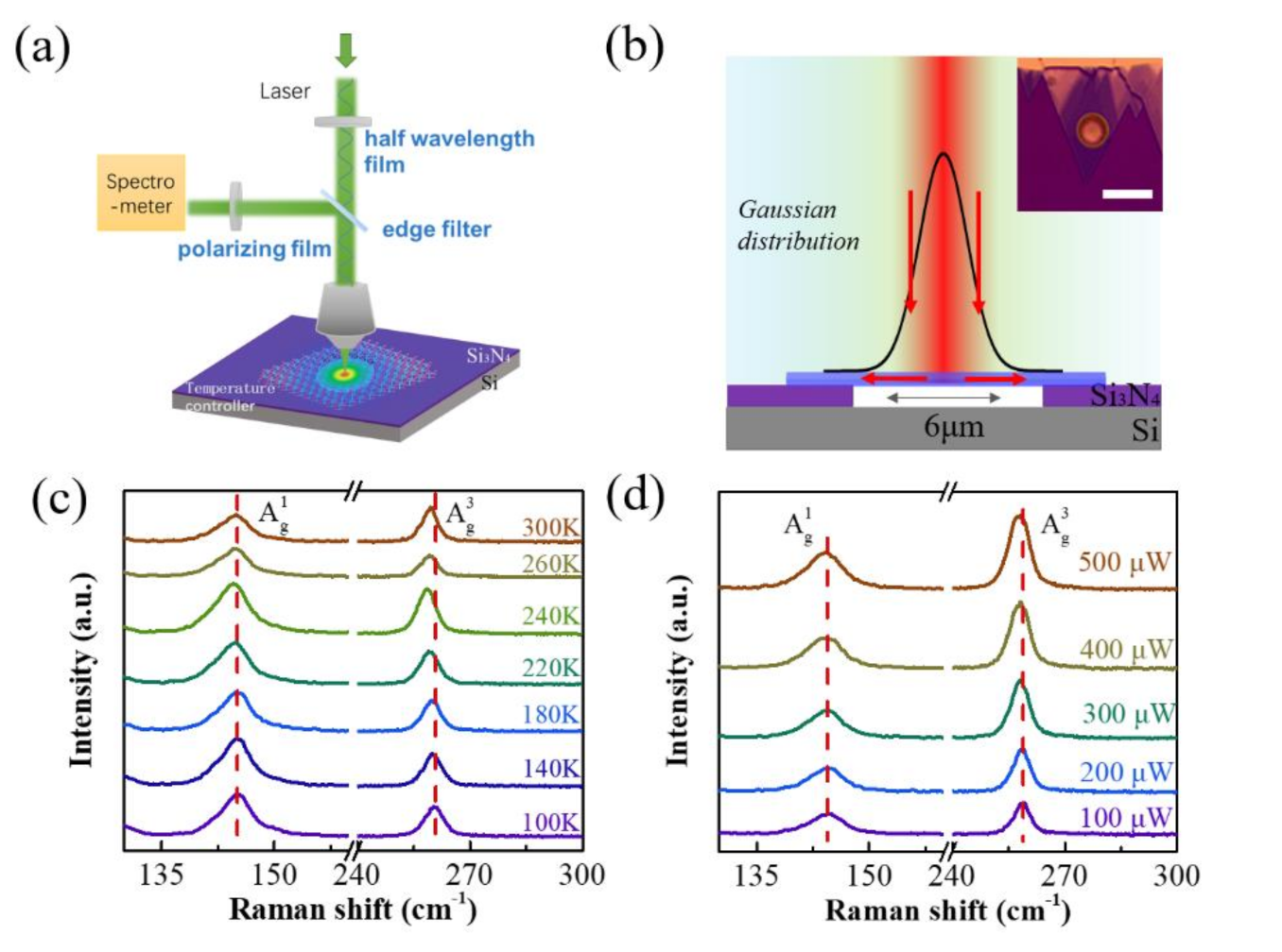
2. Materials and Methods

A single crystal of PdSe2 was purchased from HQ Graphene Company (purity = 99.998%). Few-layered PdSe2 were mechanically exfoliated from bulk crystals at room temperature. The thinner flakes were initially identified by optical microscopy (WMJ-9688), utilizing polydime-thylsiloxane (PDMS) transferred onto pre-cleaned, 200 nm Si3N4/Si with a hole of 6 μm in diameter. The atomic force microscopy (AFM) images were obtained through the non-contact mode (Hitachi, AFM5500M).
Raman spectra were obtained by the FST2-Ahdx-DZ system using an incident laser (532 nm) in the back-scattering geometry. The detector was an Andor CCD with thermoelectric cooling to −60 °C. A 50× objective (numerical aperture = 0.42) was used to focus the incident light (ei) and collect the Raman scattering (es) signal. In the parallel configuration (eies) and the cross configuration (eies), the polarization direction (ei) of the incident light was rotated every 15 degrees relative to the sample to obtain ADPRS. The temperature control was achieved by a Linkam thermal stage THMS600. The nitrogen atmosphere was maintained during the experiment to avoid the hydrolysis or oxidation of the PdSe2 nanosheet.

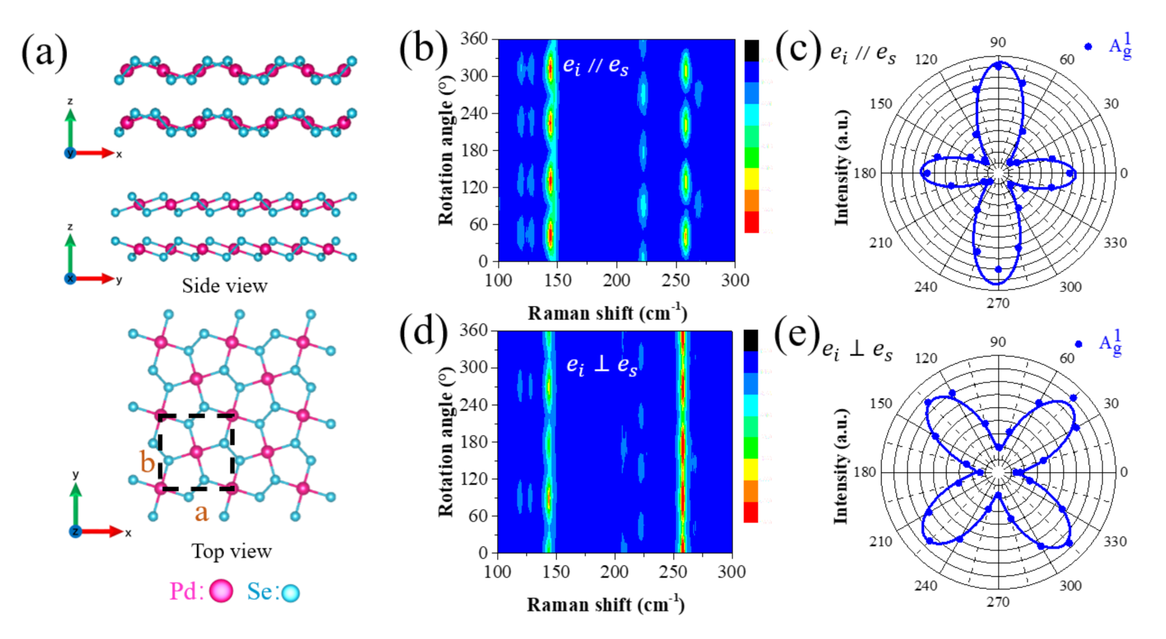
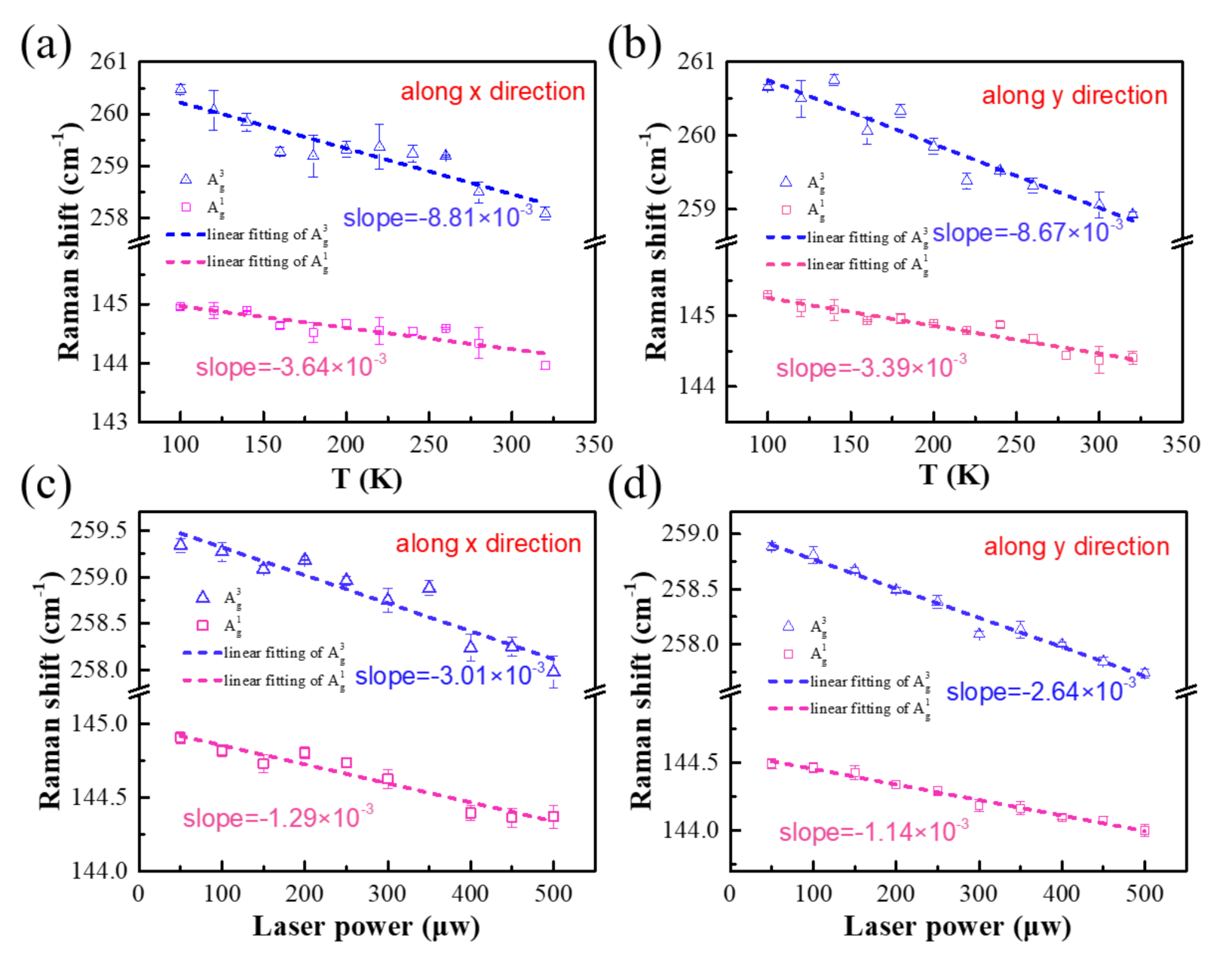
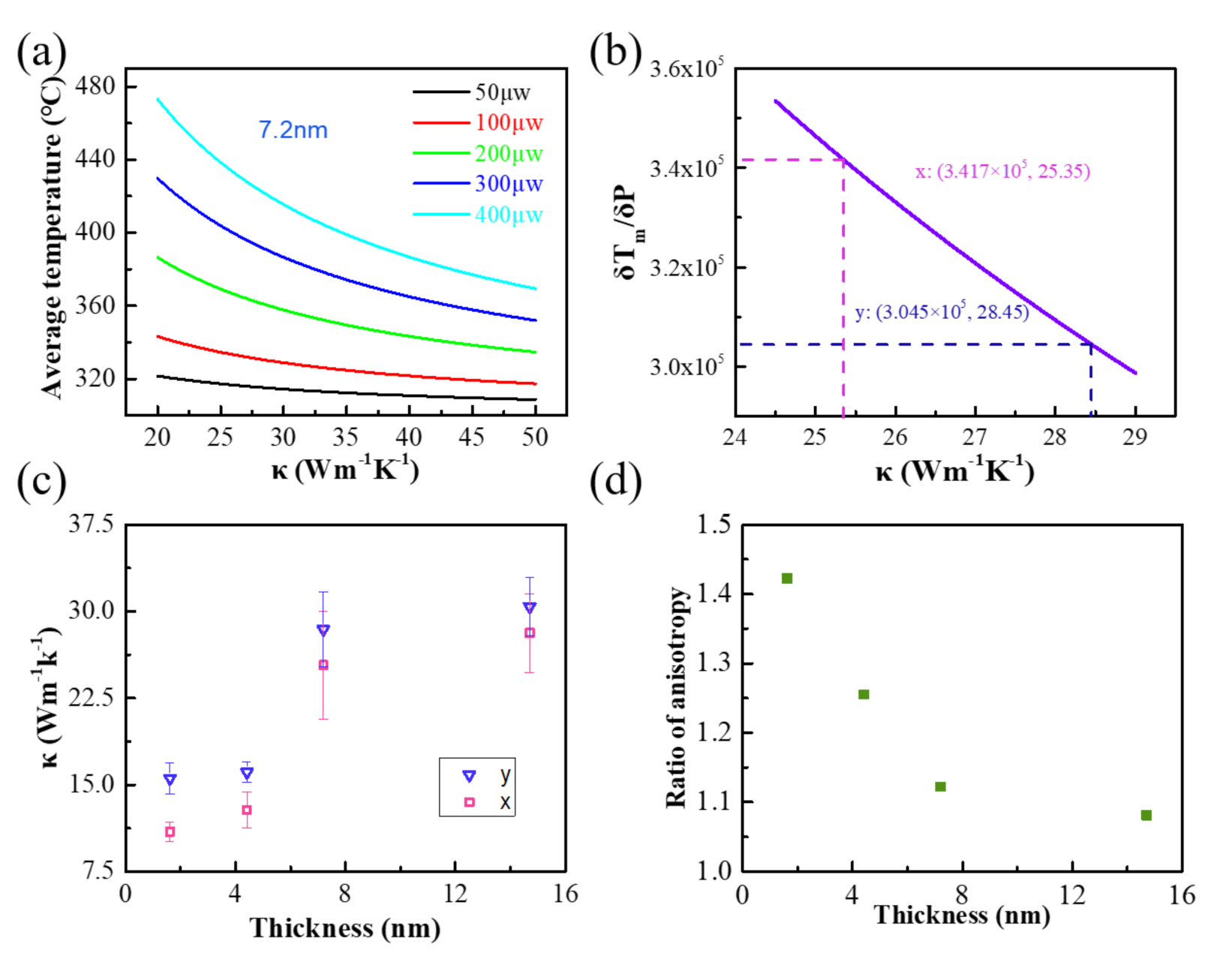
3. Results and Discussion

The bulk PdSe2 crystallizes in the space group of PbCa (point group D2h) with an orthorhombic structure and unit cell of a = 5.75 Å and b = 5.87 Å [31,32]. The pentagonal lattice structure of PdSe2 is shown in Figure 1a. The side view explicitly stresses the layered essence and the relationship of the van der Waals (vdW) forces in each layer. Pd and Se atoms show different configurations along the x- and y-directions, respectively. Typical layered structures had a single thickness of 6 Å [7], and each layer was coupled with a powerful van der Waals force (190 meV/atom) [21]. From the top view, we can see that the single layer of PdSe2 was wholly composed of a pentagon ring, exhibiting a unique pattern known as the Cairo pentagonal tiling. The pentagon has an asymmetric lattice structure and potential anisotropic physical properties exist in the plane [7,33,34]. Compared with other pentagonal 2D materials that are still in theory, PdSe2 has already shown superior performance in practical applications [35,36,37]. A typical, non-polarized Raman spectrum of exfoliated PdSe2 flakes on 200 nm Si3N4/Si substrate is shown in Figure S1 in the supplementary materials. Six prominent Raman peaks can be clearly observed. The 227 cm−1 peak can be attributed to the Bg modes, whereas the 144, 208, and 258 cm−1 peaks correspond to the Ag modes. Such a result is consistent with previous reports [38].
In order to determine lattice orientation in thermal conductivity measurements, the ADPRS was employed to understand the anisotropic phonon vibration of PdSe2. The contour map of parallel configuration is shown in Figure 1b, from which we can see that each of those peaks is shifting periodically (209 and 144 cm−1), whereas others display a four-leaf pattern (e.g., 227 and 258 cm−1). To demonstrate this phenomenon more clearly, we extracted the angle-dependent Raman intensity of a typical A g 1 mode, as shown in Figure 1c, in which the maximum intensities occurred at 90° and 270°, and the secondary maxima at 0° and 180°. In contrast to the parallel configuration, the cross configuration presented another symmetric pattern, shown in Figure 1d. Most of them exhibited a four-leaf pattern (e.g., 118, 127, 144, and 258 cm−1), and another displayed a two-leaf pattern (e.g., 208 cm−1). Unlike parallel configurations, the polar plots of the angle-dependent Raman intensity of A g 1 modes in cross configurations are shown in Figure 1e, which displays four-leaf patterns where the symmetry axis of the pattern was deflected by 45°, and the maximum intensities of all the A g 1 modes were at 45°, 135°, 225°, and 295°. The ADPRS experimental findings were in full agreement with the relationship between the Raman tensor fitting (more details can be found in the Supplementary Material Note S1) and the angle of polarization orientation. The results indicate that the two in-plane principal axes of PdSe2 can be classified by ADPRS. However, since the Raman intensity was also related to the absorption of PdSe2, the definitive a or b cannot be identified. Thus, after distinguishing the two in-plane principal axes, we employed polarized-dependent optical absorption spectra to confirm the in-plane lattice orientation [18].
Based on the unique linear dichroism transition of PdSe2, for example, Figure S2 has shown the absorption intensity at 405 and 580 nm wavelengths, which have prominent angular dependence characteristics. It is easy to define the x and y lattice directions. For example, at 405 nm, the angle of the strongest absorption intensity corresponds to the y-direction, whereas, at 580 nm, the position of the strongest absorption intensity corresponds to the x-direction. Combining the optical absorption spectrum and Raman spectrum, we can determine the x-direction corresponding to the angle with a relatively large Raman intensity in yjr A g 1 mode. These observations truly imply that the polarized Raman signals of PdSe2 are intensely dependent on its crystalline orientation. This basic non-destructive process of ensuring crystal orientation is often commonly utilized in other 2D anisotropy materials [39,40].
To find the anisotropic thermal conductivity, we employed an MRT method to systematically study the thermal conductivity of 2D PdSe2 [26,29,30]. Figure 2a shows the schematic diagram of the experimental setup, in which the polarized light was focused on the center of the hole, while the polarization direction of incident light was controlled by a rotating half-wave plate. The heat input and diffusion by the laser beam was subject to Gaussian distribution. Most heat was concentrated at the center of the suspended PdSe2. The results provide a convenient way to obtain the temperature-related phonon information. To achieve high precision, the hole under the sample was much larger than the laser spot, which can minimize the substratum’s influence and establish an appropriate temperature gradient from the hole center and the substrate. In our experiment, the hole diameter was 6 μm, which is adequate and much greater than the laser spot (about 2 μm); a typical suspended PdSe2 is shown in the inset of Figure 2b. Then, we employed a temperature-dependent Raman spectrum under parallel configuration to obtain the temperature meter, reflecting Raman spectra’s sensitivity to temperature. Embodying the temperature sensitivity of phonon vibration in PdSe2, the two most apparent Raman peaks of 7.2 nm PdSe2 are highlighted in Figure 2c. With the temperature increase from 100 K to room temperature, both the A g 1 (145 cm−1) and A g 3 (256 cm−1) modes’ peaks had a dramatic redshift, which originated from thermal expansion and anharmonic lattice vibrations [41,42]. Similarly, with the increase in laser power, the peaks of A g 1 and A g 3 modes also exhibited significant redshifts because of the laser heating effect, as shown in Figure 2d. In order to intuitively show the shift in peak position with temperature and power, we fit the peaks of A g 1 and A g 3 modes in Figure 3. The two peaks exhibited the same trend. The A g 3 peak was more apparent than the A g 1 peak, and the former’s redshift was more remarkable. This result indicates that A g 3 mode is more sensitive to temperature, so we selected the A g 3 peak shift on a microscale as the temperature meter.
The evolution of the peak frequency, ω, as a function of the temperature was linearly fit by the equation ω = ω0 + χ T, where ω0 intercepted with the temperature at 0 K and χ = δω/δT was the first order of the temperature coefficient. Figure 3a,b shows the linear fitting results of the A g 3 mode with respect to temperature in the x- and y-directions. The derived slopes related to temperature are χx = −0.00867 and χy = −0.00881 cm−1 K−1; they exhibited a lattice orientation dependence. The A g 3 peak shift was also measured as a function of laser power for the suspended PdSe2. When the laser power was increased, the noticeable Raman peak shift due to phonon softening caused by the suspended film’s temperature increased. Under a different laser power, the frequency fitting of the A g 3 mode, as shown in Figure 3d,e, derived slopes (δω/δP) in the x- and y-directions equal to −0.00301 and −0.00264 cm−1 (μW)−1, respectively. Obtaining the relationship between Raman peak shift and the calculated temperature, the average temperature (inside the laser spot) caused by the incident laser is expressed in the formula as [43]:
T m   =   0 R T r q r r d r 0 R q r r d r
where R is the radius of the hole, and r is the value of position from the center of the hole. Furthermore, we needed to consider the interfacial heat transfer and boundary conditions (see the Supplementary Material Note S2 for details). Figure 4a shows the relation between the average temperature and the thermal conductivity of the suspended films. In addition, we further obtained the expression curve of δTm/δP and the thermal conductivity, as shown in Figure 4b, which was easily obtained by our experiment.
From the above discussion, the thermal conductivity of 7.2 nm thickness PdSe2 along the x- and y-directions were calculated to be 28.45 and 25.35 W m−1 K−1, respectively. The extracted thickness-dependent thermal conductivity is shown in Figure 4c, indicating the existence of robust anisotropy in the few-layered PdSe2, with an anisotropy ratio as high as 1.42 (for the calculation of the error bar, see the Supplementary Material Note S3). Such thickness-dependent anisotropic thermal conductivity has been observed in few-layered Te and BP [29,30]. By increasing the thickness of PdSe2, the anisotropy of thermal conductivity decreased gradually in the in-plane, as shown in Figure 4d. (The thickness was determined by AFM, as shown in Figure S3). The thermal conductivity ratio (κx/κy) decreased from 1.42 to 1.08 because of the thermal conductivity in the x-direction but increased faster than the y-direction with increasing thickness. This size effect resulted from strong surface scattering of longer mean-free-path phonons [30]. The relatively thinner PdSe2 had a lower group velocity and a longer phonon lifetime and was more likely to be affected by surface defects. The anisotropic thermal conductivity was mainly attributed to phonon scattering along the x-direction more than the y-direction, and the anisotropy of phonon scattering decreases with an increase in thickness [22]. The strong size effects on thermal and electric transport due to surface scattering were also observed in Bi2Te3 thermoelectric material [44]. In particular, as for the heat diffusion in the direction of the z-axis, the strong interlayer action of PdSe2 may affect the experimental measurement, which requires further investigation. To get an intuitive understanding of the in-plane anisotropic thermal conductivity in PdSe2, Table 1 summarizes the thermal conductivity of anisotropic 2D materials studied in recent years. Based on our work, the anisotropic thermal conductivity ratio of PdSe2 was relatively large among the reported 2D materials. In contrast to previous theoretical reports [22], our experimental data are slightly higher than theoretical calculations but still on the same order of magnitude. The possible reason is the uncertainty of interfacial heat transfer between the material and the substrate [45]. However, for low-thermal-conductivity materials, most of the laser heat caused by a small speckle is concentrated in the hole, which has a minimal effect on the results.

4. Conclusions

To conclude, we investigated the anisotropic in-plane thermal conductivity of the suspended 2D PdSe2 through Raman spectroscopy. The anisotropic thermal conductivity in low-symmetry pentagonal 2D PdSe2 was first demonstrated in our experiment. We engaged linear polarization-dependent Raman spectroscopy and absorption spectrum to determine the crystal orientation (x- and y-directions) of PdSe2 flakes due to the strong direction dependence of the anisotropic structure. The prominent anisotropy ratio of the thermal conductivity of PdSe2 flakes measured by MRT was found to be 1.42. This result provides a valuable reference for anisotropic thermoelectric applications. Our study may play a ground-breaking position regarding the anisotropic in-plane thermal conductivity of PdSe2, which will greatly facilitate applications in energy conversion and in electronic devices.

Supplementary Materials

The following are available online at https://www.mdpi.com/article/10.3390/su13084155/s1. Figure S1: Typical Raman spectra of PdSe2, Figure S2: Polarized light absorption spectrum, Figure S3. Optical imaging and AFM height profiles of suspended few-layered PdSe2, Note S1: Raman tensors fitting, Note S2: Determination of the average temperature profile through the boundary conditions, Note S3: The error bar of thermal conductance.

Author Contributions

Conceptualization, L.C. and L.L.; methodology, L.C., W.Z. and L.L.; data curation, L.C.; writing—original draft preparation, L.C., J.C., C.T., S.Y., G.L., Y.Z., P.G., and L.L.; writing—review and editing, L.C., W.Z., H.Z., J.C., C.T., S.Y., G.L., Y.Z., P.G., and L.L.; project administration, L.L.; funding acquisition, L.L. All authors have read and agreed to the published version of the manuscript.

Funding

This research was funded by the National Natural Science Foundation of China (Grant No. 51902001, 11904154), the Recruitment Program for Leading Talent Team of Anhui Province (2019-16), the Anhui Provincial Natural Science Foundation (1908085QE17), the Anhui Province Natural Science Foundation (No. 1908085MF222), and the Foundation of the State Key Laboratory of Pulsed Power Laser Technology (No. SKL2019ZR04).

Institutional Review Board Statement

Not applicable.

Informed Consent Statement

Not applicable.

Data Availability Statement

Not applicable.

Conflicts of Interest

The authors declare no conflict of interest.

References

  1. Novoselov, K.S.; Geim, A.K.; Morozov, S.V.; Jiang, D.; Zhang, Y.; Dubonos, S.V.; Grigorieva, I.V.; Firsov, A.A. Electric Field Effect in Atomically Thin Carbon Films. Science 2004, 306, 666–669. [Google Scholar] [CrossRef] [Green Version]
  2. Wang, Q.H.; Kalantar-Zadeh, K.; Kis, A.; Coleman, J.N.; Strano, M.S. Electronics and optoelectronics of two-dimensional transition metal dichalcogenides. Nat. Nanotechnol. 2012, 7, 699–712. [Google Scholar] [CrossRef]
  3. Li, L.; Han, W.; Pi, L.; Niu, P.; Han, J.; Wang, C.; Su, B.; Li, H.; Xiong, J.; Bando, Y.; et al. Emerging in—Plane anisotropic two—Dimensional materials. InfoMat 2019, 1, 54–73. [Google Scholar] [CrossRef]
  4. Ma, W.; Shabbir, B.; Ou, Q.; Dong, Y.; Chen, H.; Li, P.; Zhang, X.; Lu, Y.; Bao, Q. Anisotropic polaritons in van der Waals materials. InfoMat 2020, 2, 777–790. [Google Scholar] [CrossRef]
  5. Ciarrocchi, A.; Avsar, A.; Ovchinnikov, D.; Kis, A. Thickness-modulated metal-to-semiconductor transformation in a transition metal dichalcogenide. Nat. Commun. 2018, 9, 919. [Google Scholar] [CrossRef] [PubMed]
  6. Wang, Y.; Li, L.; Yao, W.; Song, S.; Sun, J.T.; Pan, J.; Ren, X.; Li, C.; Okunishi, E.; Wang, Y.Q.; et al. Monolayer PtSe2, a New Semiconducting Transition-Metal-Dichalcogenide, Epitaxially Grown by Direct Selenization of Pt. Nano Lett. 2015, 15, 4013–4018. [Google Scholar] [CrossRef]
  7. Oyedele, A.D.; Yang, S.; Liang, L.; Puretzky, A.A.; Wang, K.; Zhang, J.; Yu, P.; Pudasaini, P.R.; Ghosh, A.W.; Liu, Z.; et al. PdSe2: Pentagonal Two-Dimensional Layers with High Air Stability for Electronics. J. Am. Chem. Soc. 2017, 139, 14090–14097. [Google Scholar] [CrossRef] [PubMed]
  8. Liang, Q.; Wang, Q.; Zhang, Q.; Wei, J.; Lim, S.X.; Zhu, R.; Hu, J.; Wei, W.; Lee, C.; Sow, C.; et al. High-Performance, Room Temperature, Ultra-Broadband Photodetectors Based on Air-Stable PdSe2. Adv. Mater. 2019, 31, 1807609. [Google Scholar] [CrossRef]
  9. Cheng, P.K.; Tang, C.Y.; Ahmed, S.; Qiao, J.; Zeng, L.H.; Tsang, Y.H. Utilization of group 10 2D TMDs-PdSe2 as a nonlinear optical material for obtaining switchable laser pulse generation modes. Nanotechnology 2021, 32, 055201. [Google Scholar] [CrossRef]
  10. Di Bartolomeo, A.; Pelella, A.; Liu, X.; Miao, F.; Passacantando, M.; Giubileo, F.; Grillo, A.; Iemmo, L.; Urban, F.; Liang, S.J. Pressure—Tunable Ambipolar Conduction and Hysteresis in Thin Palladium Diselenide Field Effect Transistors. Adv. Funct. Mater. 2019, 29, 1902483. [Google Scholar] [CrossRef]
  11. Li, L.; Wang, W.; Chai, Y.; Li, H.; Tian, M.; Zhai, T. Few-Layered PtS2 Phototransistor on h-BN with High Gain. Adv. Funct. Mater. 2017, 27, 1701011. [Google Scholar] [CrossRef]
  12. Liu, G.; Zeng, Q.; Zhu, P.; Quhe, R.; Lu, P. Negative Poisson’s ratio in monolayer PdSe2. Comput. Mater. Sci. 2019, 160, 309–314. [Google Scholar] [CrossRef]
  13. Lei, W.; Cai, B.; Zhou, H.; Heymann, G.; Tang, X.; Zhang, S.; Ming, X. Ferroelastic lattice rotation and band-gap engineering in quasi 2D layered-structure PdSe2 under uniaxial stress. Nanoscale 2019, 11, 12317–12325. [Google Scholar] [CrossRef]
  14. Hellgren, N.; Berlind, T.; Gueorguiev, G.K.; Johansson, M.P.; Stafström, S.; Hultman, L. Fullerene-like BCN thin films: A computational and experimental study. Mater. Sci. Eng. B 2004, 113, 242–247. [Google Scholar] [CrossRef]
  15. Goyenola, C.; Stafström, S.; Hultman, L.; Gueorguiev, A.G.K. Structural Patterns Arising during Synthetic Growth of Fullerene-Like Sulfocarbide. J. Phys. Chem. C 2012, 116, 21124–21131. [Google Scholar] [CrossRef]
  16. Zhang, G.; Amani, M.; Chaturvedi, A.; Tan, C.; Bullock, J.; Song, X.; Kim, H.; Lien, D.-H.; Scott, M.C.; Zhang, H.; et al. Optical and electrical properties of two-dimensional palladium diselenide. Appl. Phys. Lett. 2019, 114, 253102. [Google Scholar] [CrossRef] [Green Version]
  17. Jiang, S.; Xie, C.; Gu, Y.; Zhang, Q.; Wu, X.; Sun, Y.; Li, W.; Shi, Y.; Zhao, L.; Pan, S.; et al. Anisotropic Growth and Scanning Tunneling Microscopy Identification of Ultrathin Even-Layered PdSe2 Ribbons. Small 2019, 15, 1902789. [Google Scholar] [CrossRef] [PubMed]
  18. Yu, J.; Kuang, X.; Gao, Y.; Wang, Y.; Chen, K.; Ding, Z.; Liu, J.; Cong, C.; He, J.; Liu, Z.; et al. Direct Observation of the Linear Dichroism Transition in Two-Dimensional Palladium Diselenide. Nano Lett. 2020, 20, 1172–1182. [Google Scholar] [CrossRef]
  19. Zhong, J.; Yu, J.; Cao, L.; Zeng, C.; Ding, J.; Cong, C.; Liu, Z.; Liu, Y. High-performance polarization-sensitive photodetector based on a few-layered PdSe2 nanosheet. Nano Res. 2020, 13, 1780–1786. [Google Scholar] [CrossRef]
  20. Xu, W.; Jiang, J.; Ma, H.; Zhang, Z.; Li, J.; Zhao, B.; Wu, R.; Yang, X.; Zhang, H.; Li, B.; et al. Vapor phase growth of two-dimensional PdSe2 nanosheets for high-photoresponsivity near-infrared photodetectors. Nano Res. 2020, 13, 2091–2097. [Google Scholar] [CrossRef]
  21. Sun, J.; Shi, H.; Siegrist, T.; Singh, D.J. Electronic, transport, and optical properties of bulk and mono-layer PdSe2. Appl. Phys. Lett. 2015, 107, 153902. [Google Scholar] [CrossRef]
  22. Lan, Y.-S.; Chen, X.-R.; Hu, C.-E.; Cheng, Y.; Chen, Q.-F. Penta-PdX2 (X = S, Se, Te) monolayers: Promising anisotropic thermoelectric materials. J. Mater. Chem. A 2019, 7, 11134–11142. [Google Scholar] [CrossRef]
  23. Zhao, Y.; Yu, P.; Zhang, G.; Sun, M.; Chi, D.; Hippalgaonkar, K.; Thong, J.T.L.; Wu, J. Low—Symmetry PdSe2 for High Performance Thermoelectric Applications. Adv. Funct. Mater. 2020, 30, 2004896. [Google Scholar] [CrossRef]
  24. Qin, D.; Yan, P.; Ding, G.; Ge, X.; Song, H.; Gao, G. Monolayer PdSe2: A promising two-dimensional thermoelectric material. Sci. Rep. 2018, 8, 2764. [Google Scholar] [CrossRef] [PubMed]
  25. Sun, M.; Chou, J.P.; Shi, L.; Gao, J.; Hu, A.; Tang, W.; Zhang, G. Few-Layer PdSe2 Sheets: Promising Thermoelectric Materials Driven by High Valley Convergence. ACS Omega 2018, 3, 5971–5979. [Google Scholar] [CrossRef]
  26. Chen, Y.; Peng, B.; Cong, C.; Shang, J.; Wu, L.; Yang, W.; Zhou, J.; Yu, P.; Zhang, H.; Wang, Y.; et al. In-Plane Anisotropic Thermal Conductivity of Few-Layered Transition Metal Dichalcogenide Td-WTe2. Adv. Mater. 2019, 31, 1804979. [Google Scholar] [CrossRef]
  27. Wang, T.; Han, M.; Wang, R.; Yuan, P.; Xu, S.; Wang, X. Characterization of anisotropic thermal conductivity of suspended nm-thick black phosphorus with frequency-resolved Raman spectroscopy. J. Appl. Phys. 2018, 123, 145104. [Google Scholar] [CrossRef] [Green Version]
  28. Soini, M.; Zardo, I.; Uccelli, E.; Funk, S.; Koblmüller, G.; Fontcuberta i Morral, A.; Abstreiter, G. Thermal conductivity of GaAs nanowires studied by micro-Raman spectroscopy combined with laser heating. Appl. Phys. Lett. 2010, 97, 263107. [Google Scholar] [CrossRef]
  29. Luo, Z.; Maassen, J.; Deng, Y.; Du, Y.; Garrelts, R.P.; Lundstrom, M.S.; Ye, P.D.; Xu, X. Anisotropic in-plane thermal conductivity observed in few-layer black phosphorus. Nat. Commun. 2015, 6, 8572. [Google Scholar] [CrossRef]
  30. Huang, S.; Segovia, M.; Yang, X.; Koh, Y.R.; Wang, Y.; Ye, P.D.; Wu, W.; Shakouri, A.; Ruan, X.; Xu, X. Anisotropic thermal conductivity in 2D tellurium. 2D Mater. 2019, 7, 015008. [Google Scholar] [CrossRef]
  31. Puretzky, A.A.; Oyedele, A.D.; Xiao, K.; Haglund, A.V.; Sumpter, B.G.; Mandrus, D.; Geohegan, D.B.; Liang, L. Anomalous interlayer vibrations in strongly coupled layered PdSe2. 2D Mater. 2018, 5, 035016. [Google Scholar] [CrossRef]
  32. Zeng, L.-H.; Wu, D.; Lin, S.-H.; Xie, C.; Yuan, H.-Y.; Lu, W.; Lau, S.P.; Chai, Y.; Luo, L.-B.; Li, Z.-J.; et al. Controlled Synthesis of 2D Palladium Diselenide for Sensitive Photodetector Applications. Adv. Funct. Mater. 2019, 29, 1806878. [Google Scholar] [CrossRef] [Green Version]
  33. Grønvold, F.; Røst, E. The crystal structure of PdSe2 and PdS2. Acta Crystallogr. 1957, 10, 329–331. [Google Scholar] [CrossRef]
  34. Zhang, S.; Zhou, J.; Wang, Q.; Chen, X.; Kawazoe, Y.; Jena, P. Penta-graphene: A new carbon allotrope. Proc. Natl. Acad. Sci. USA 2015, 112, 2372–2377. [Google Scholar] [CrossRef] [PubMed] [Green Version]
  35. Li, X.; Meng, S.; Sun, J.-T. Emergence of d-orbital magnetic Dirac fermions in a MoS2 monolayer with squared pentagon structure. Phys. Rev. B 2020, 101, 144409. [Google Scholar] [CrossRef]
  36. Wu, P. The Study for Two-dimensional PtX2 (X = S Se Te) Which Have Geometrical Structures Fully Composed of Pentagons. IOP Conf. Ser. Mater. Sci. Eng. 2019, 631, 042010. [Google Scholar] [CrossRef]
  37. Yang, H.; Li, Y.; Yang, Z.; Shi, X.; Lin, Z.; Guo, R.; Xu, L.; Qu, H.; Zhang, S. First-principles calculations of the electronic properties of two-dimensional pentagonal structure XS2 (X = Ni, Pd, Pt). Vacuum 2020, 174, 109176. [Google Scholar] [CrossRef]
  38. Long, M.; Wang, Y.; Wang, P.; Zhou, X.; Xia, H.; Luo, C.; Huang, S.; Zhang, G.; Yan, H.; Fan, Z.; et al. Palladium Diselenide Long-Wavelength Infrared Photodetector with High Sensitivity and Stability. ACS Nano 2019, 13, 2511–2519. [Google Scholar] [CrossRef] [Green Version]
  39. Wang, J.; Zhou, Y.J.; Xiang, D.; Ng, S.J.; Watanabe, K.; Taniguchi, T.; Eda, G. Polarized Light-Emitting Diodes Based on Anisotropic Excitons in Few-Layer ReS2. Adv. Mater. 2020, 32, 2001890. [Google Scholar] [CrossRef]
  40. Li, L.; Wang, W.; Gong, P.; Zhu, X.; Deng, B.; Shi, X.; Gao, G.; Li, H.; Zhai, T. 2D GeP: An Unexploited Low-Symmetry Semiconductor with Strong In-Plane Anisotropy. Adv. Mater. 2018, 30, 1706771. [Google Scholar] [CrossRef]
  41. Sahoo, S.; Gaur, A.P.S.; Ahmadi, M.; Guinel, M.J.F.; Katiyar, R.S. Temperature-Dependent Raman Studies and Thermal Conductivity of Few-Layer MoS2. J. Phy. Chem. C 2013, 117, 9042–9047. [Google Scholar] [CrossRef] [Green Version]
  42. Araujo, F.D.V.; Oliveira, V.V.; Gadelha, A.C.; Carvalho, T.C.V.; Fernandes, T.F.D.; Silva, F.W.N.; Longuinhos, R.; Ribeiro-Soares, J.; Jorio, A.; Souza Filho, A.G.; et al. Temperature-dependent phonon dynamics and anharmonicity of suspended and supported few-layer gallium sulfide. Nanotechnology 2020, 31, 495702. [Google Scholar] [CrossRef] [PubMed]
  43. Cai, W.; Moore, A.L.; Zhu, Y.; Li, X.; Chen, S.; Shi, L.; Ruoff, R.S. Thermal transport in suspended and supported monolayer graphene grown by chemical vapor deposition. Nano Lett. 2010, 10, 1645–1651. [Google Scholar] [CrossRef] [PubMed]
  44. Pettes, M.T.; Maassen, J.; Jo, I.; Lundstrom, M.S.; Shi, L. Effects of surface band bending and scattering on thermoelectric transport in suspended bismuth telluride nanoplates. Nano Lett. 2013, 13, 5316–5322. [Google Scholar] [CrossRef]
  45. Peimyoo, N.; Shang, J.; Yang, W.; Wang, Y.; Cong, C.; Yu, T. Thermal conductivity determination of suspended mono- and bilayer WS2 by Raman spectroscopy. Nano Res. 2014, 8, 1210–1221. [Google Scholar] [CrossRef]
  46. Liu, H.; Yu, X.; Wu, K.; Gao, Y.; Tongay, S.; Javey, A.; Chen, L.; Hong, J.; Wu, J. Extreme In-Plane Thermal Conductivity Anisotropy in Titanium Trisulfide Caused by Heat-Carrying Optical Phonons. Nano Lett. 2020, 20, 5221–5227. [Google Scholar] [CrossRef]
  47. Jang, H.; Ryder, C.R.; Wood, J.D.; Hersam, M.C.; Cahill, D.G. 3D Anisotropic Thermal Conductivity of Exfoliated Rhenium Disulfide. Adv. Mater. 2017, 29, 1700650. [Google Scholar] [CrossRef]
Figure 1. (a) Typical side view (up) and top view (down) of the layered, PdSe2 anisotropic crystal structure. The contour maps of the angle–dependent polarized Raman spectra (ADPRS) of a PdSe2 flake under (b) parallel–polarized and (d) cross–polarized configurations. Polar plots and fit curves of A g 1 peak intensities under (c) parallel–polarized and (e) cross–polarized configurations.
Sustainability 13 04155 g001
Figure 2. (a) Schematic diagram of the experimental setup for the thermal conductivity measurements. (b) Schematic of the suspended PdSe2 on a hole 6 μm in diameter. The bar in the inset is 10 μm. (c,d) Temperature–dependent and incident–laser–power–dependent Raman spectra of the 7.2 nm-thick suspended PdSe2 with incident laser polarization fixed along the x– and y–directions.
Sustainability 13 04155 g002
Figure 3. (a,b) were the A g 1 and A g 3 peak frequencies as a function of temperature along x– and y–directions, respectively. (c,d) were the A g 1 peak frequencies as a function of laser power along the x– and y–directions, respectively.
Sustainability 13 04155 g003
Figure 4. (a) The average temperature versus the thermal conductivity of the suspended, 7.2 nm–thick PdSe2 nanosheet at different laser powers. (b) The calculated curve of δTm/δP as a function of the thermal conductivity. The thermal conductivity along the x– and y–directions were extracted by experimental measure. (c) The extracted in–plane thermal conductivity of different thicknesses. (d) The anisotropic ratio of thermal conductivity versus the thickness of PdSe2.
Sustainability 13 04155 g004
Table 1. Thermal conductivities of anisotropic 2D materials compared.
MaterialFabricationThickness (nm)MethodIn-Plane κ (W m−1 K−1)RatioResource
Td-WTe2Exfoliation11.2Micro-Raman thermometry (MRT)0.6390.7431.16Ref. [26]
TiS3Exfoliation100Thermal bridge2.845.782.04Ref. [46]
TeSolution phase syntheses100MRT1.72.151.26Ref. [30]
BPExfoliation9.5MRT~10~202.00Ref. [29]
ReS2Exfoliation150Time-domaint
hermoreflectance (TDTR)
50701.40Ref. [47]
PdSe2Exfoliation1.62MRT10.9515.581.42This study
Publisher’s Note: MDPI stays neutral with regard to jurisdictional claims in published maps and institutional affiliations.

