Article

Phenyl-C61-Butyric Acid Methyl Ester Hybrid Solution for Efficient CH3NH3PbI3 Perovskite Solar Cells

1
Department of Physics, Kunsan National University, Gunsan 54150, Korea
2
KU-KIST Green School, Graduate School of Energy and Environment, Korea University, Seoul 02841, Korea
*
Authors to whom correspondence should be addressed.
Sustainability 2019, 11(14), 3867; https://doi.org/10.3390/su11143867
Submission received: 29 May 2019 / Revised: 28 June 2019 / Accepted: 15 July 2019 / Published: 16 July 2019

Abstract

:
Organic–inorganic halide perovskite solar cells (PSCs) have excellent chemical, electronic, and optical properties, making them attractive next-generation thin-film solar cells. Typical PSCs were fabricated with a perovskite absorber layer between the TiO2 electron-transport layer (ETL) and the 2,2′,7,7′-tetrakis-(N,N-di-4-methoxyphenylamino)-9,9′-spirobifluorene (Spiro-OMeTAD) hole-transport layer (HTL). We examined the influence of phenyl-C61-butyric acid methyl ester (PCBM) on the PSC device. PSCs using the PCBM layer as an ETL were investigated, and the absorber layer was coated by dissolving PCBM in a methyl ammonium lead iodide (MAPbI3) precursor solution to examine the changes at the perovskite interface and inside the perovskite absorber layer. The PSCs fabricated by adding a small amount of PCBM to the MAPbI3 solution exhibited a significantly higher maximum efficiency of 16.55% than conventional PSCs (14.34%). Fabricating the PCBM ETL and PCBM-MAPbI3 hybrid solid is expected to be an efficient route for improving the photovoltaic performance.

1. Introduction

As energy consumption increases throughout the world, solar cells are expected to be a key technology for solving the energy problem, and organic–inorganic hybrid metal halides are emerging as a new class of absorber materials for solar-cell devices. Organic–inorganic halide perovskite solar cells (PSCs) are important candidates for thin-film solar cells owing to their low cost and high performance. Additionally, PSCs are widely considered as promising and next-generation photovoltaic devices [1,2,3]. The main advantages of PSCs are their low production cost and high efficiency. Another advantage of PSCs is that they are based on flexible, lightweight, and semi-transparent thin films [4,5,6,7,8,9]. PSCs have a light-absorber layer with an organic–inorganic hybrid perovskite crystal structure—typically methyl-ammonium lead tri-iodide (CH3NH3PbI3, MAPbI3)—fabricated on a transparent conductive oxide coated substrate. In a typical PSC, the device structure consists of a perovskite absorber layer that converts photons into electron/hole pairs in a photoactive layer, between the electron-transport layer (ETL) as transport photo-generated electrons and the hole-transport layer (HTL) as transport holes. N-type and p-type semiconductor materials have also been used for the ETL and HTL because they efficiently extract the photoexcited electrons and holes from the perovskite, respectively, which are transported to and then collected by a transparent, conducting oxide-coated glass substrate. Most high-efficiency PSCs include TiO2 as an ETL and 2,2′,7,7′-tetrakis-(N,N-di-4-methoxyphenylamino)-9,9′-spirobifluorene (Spiro-OMeTAD) as an HTL. However, TiO2 and Spiro-OMeTAD materials exhibit poor stability under ultraviolet (UV) light irradiation and with unfavorable moisture and temperature conditions, respectively. Therefore, alternate materials have recently been intensively studied for enhancing the stability of PSCs. Among them, phenyl-C61-butyric acid methyl ester (PCBM) has been widely used for PSCs owing to its simple coating, small hysteresis effect, and high device performance as an ETL layer [10,11,12,13]. Recently, Huang et al. reported the PCBM passivation effect, where the C61 fullerene diffuses into the perovskite layer through the grain boundaries and further passivates the shallow trap state [14].
In the present study, we investigated the performance change of a PSC device when PCBM was mixed in the light absorber layer. PSCs with a PCBM layer as an ETL were also studied, and the absorber layer was coated by dissolving PCBM in a perovskite precursor solution (PCBM-MAPbI3 hybrid solution) to investigate the changes at the perovskite interface and inside the perovskite absorber layer. According to the amount of PCBM in the MAPbI3 precursor solution, the microstructures of the perovskite absorber layer were investigated. A low content of PCBM in the MAPbI3 precursor solution yielded efficient electron transport, improving the charge-carrier extraction and transport. Therefore, a higher device efficiency (16.55%) was achieved compared to that of the conventional device (14.34%, without PCBM). This study provides a simple and practical route for improving photovoltaic performance.

2. Materials and Methods

2.1. Materials

To prepare the perovskite precursor, commercial material powders were used such as methylammonium iodide (MAI; 99%) and lead (II) iodide (PbI2; 99.9985%). N,N-dimethylformamide (DMF; 99.8%) was used as the main solvent. To prepare the PCBM precursor solution, chlorobenzene (CB; 99.8%) and PCBM (99.9%) were used. To prepare the TiO2 solution, 0.15 M titanium diisopropoxide dis(acetylacetonate) (75 wt% in isopropanol) was mixed in 1-butanol (99.8%). The Spiro-OMeTAD solution consisted of 72.3 mg Spiro-OMeTAD, 28.8 μl of 4-tert-butyl pyridine, and 17.5 μl of lithium bis(trifluoromethanesulfonyl)imide (Li-TFSI) solution in 1 ml CB. All chemicals were used as received, without any further purification.

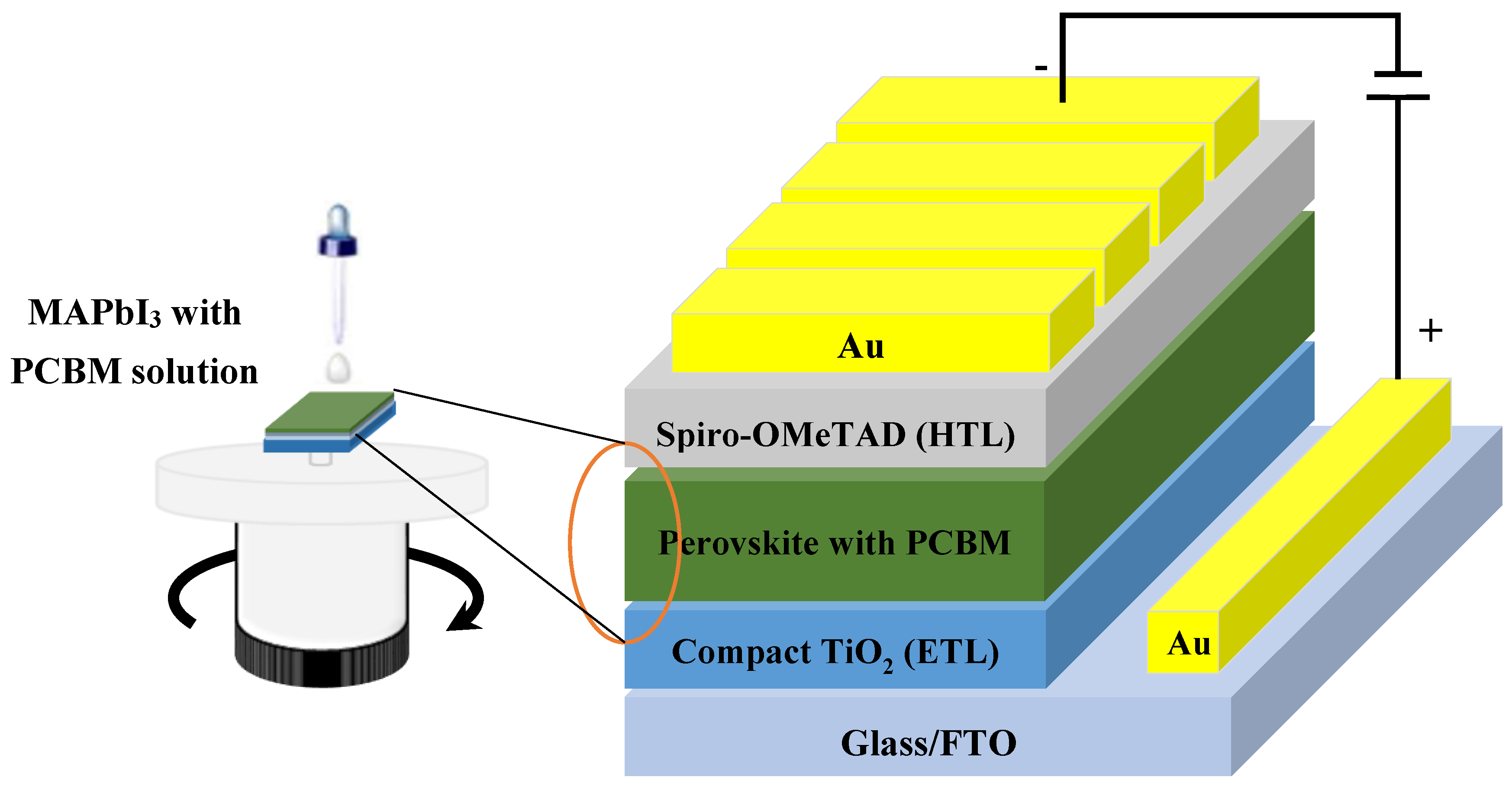
2.2. Film Formation and Device Fabrication Procedure of n-i-p Perovskite Solar Cells (PSCs)

The fabrication process is described as follows. The patterned fluorine-doped tin oxide (FTO) coated glass substrates were washed with an alkaline detergent. Then, the FTO glass substrates were sequentially ultrasonically cleaned with acetone (15 min), ethyl alcohol (15 min), and isopropyl alcohol (15 min) and rinsed with deionized water. After the glass substrate was dried by a N2 flow, UV-ozone (UVO) treatment was applied for 20 min to remove any organic residue. A TiO2 solution as ETL was spin-coated onto the FTO substrate at 700 rpm for 8 s, 1000 rpm for 10 s, and 2000 rpm for 40 s, and then the substrates were annealed at 125 °C for 5 min in atmospheric air. This procedure was repeated three times to form an TiO2 ETL with the appropriate thickness (about 128 nm). The TiO2 was heated at 450 °C for 1 h to obtain an anatase crystal structure having a favorable crystal structure of the ETL layer, and then UVO treatment was applied again for 20 min. The MAPbI3 was spin-coated via a one-step process in a dry N2 ambient glovebox. The MAPbI3 solution, which contained 461 mg of PbI2, 159 mg of MAI, and 78 mg of dimethyl sulfoxide (DMSO) (molar ratio 1:1:1), was mixed in 600 mg of a DMF solution. Additionally, PCBM solutions were prepared by adding 20 mg of PCBM to 1 mL of CB. The PCBM solutions were directly mixed into the MAPbI3 solution. The PCBM-MAPbI3 hybrid solution was stirred at 70 °C for 1 h before spin-coating, and the volume ratios of MAPbI3:PCBM were 1:1, 1:0.5, 1:0.1, 1:0.05, 1:0.01, and 1:0.005. The PCBM-MAPbI3 hybrid solution with the 1:1 volume ratio was not well mixed; thus, the mixture was stirred overnight at 70 °C and then spin-coated. The PCBM-MAPbI3 solutions were spin-coated at 4000 rpm for 25 s as the absorber layer of the solar cells, followed by annealing at 65 °C for 1 min and at 100 °C for 2 min to remove residual solvents. Next, Spiro-OMeTAD solution was coated onto the perovskite absorber layer at 3000 rpm for 30 s. Finally, device fabrication was completed via the deposition of Au electrodes using a sputtering system. The detailed experimental methods for the device fabrication are presented in other papers [15,16].
The device structure is shown in Figure 1. Only MAPbI3 (the most common perovskite light-absorber material) and MAPbI3+PCBM mixed film were used as the solar cell absorber layer. The TiO2 and Spiro-OMeTAD were used for the ETL and HTL, respectively. All the experimental perovskite photovoltaic devices had a normal (n-i-p) planar heterojunction structure.

2.3. Characterizations

The structural properties of the perovskite films were measured and analyzed via high-resolution X-ray diffraction (HR-XRD). The thermal properties of the PCBM-MAPbI3 hybrid solution were verified using thermogravimetry and differential thermal analysis (TG-DTA). The chemical properties of PCBM-MAPBI3 hybrid film were measured by Fourier-transform infrared spectroscopy (FTIR). Additionally, energy-dispersive X-ray spectroscopy (EDS) mapping was performed to elucidate the PCBM’s location. To evaluate the quality of the absorber layer, we measured the photoluminescence (PL) and time-resolved PL (TRPL) of the MAPbI3 films and PCBM-MAPbI3 hybrid films with various PCBM contents (volume ratio from 0.5% to 100%). Current density–voltage (J–V) characterization of the PSCs was performed using a Keithley 2400 source meter under AM 1.5G 1-sun illumination. The illumination was calibrated using standard Si solar cells and a photometer.

3. Results and Discussion

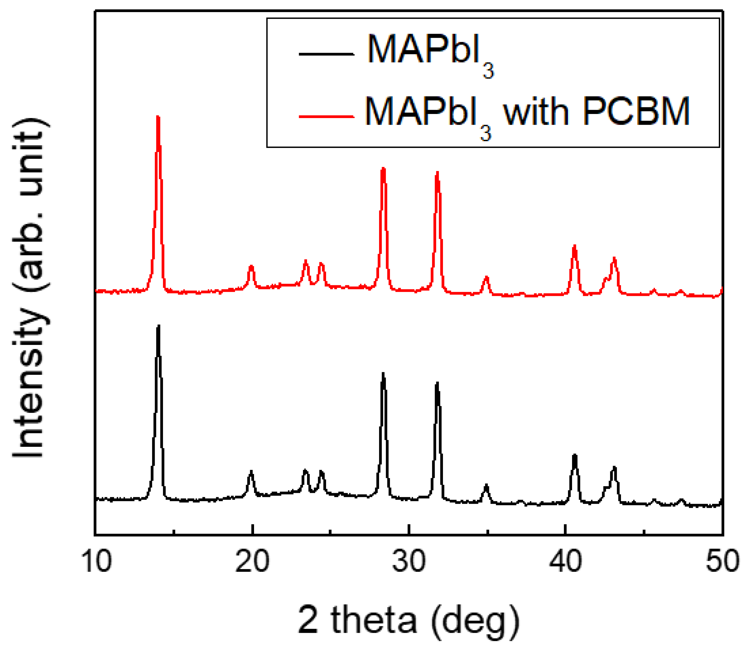
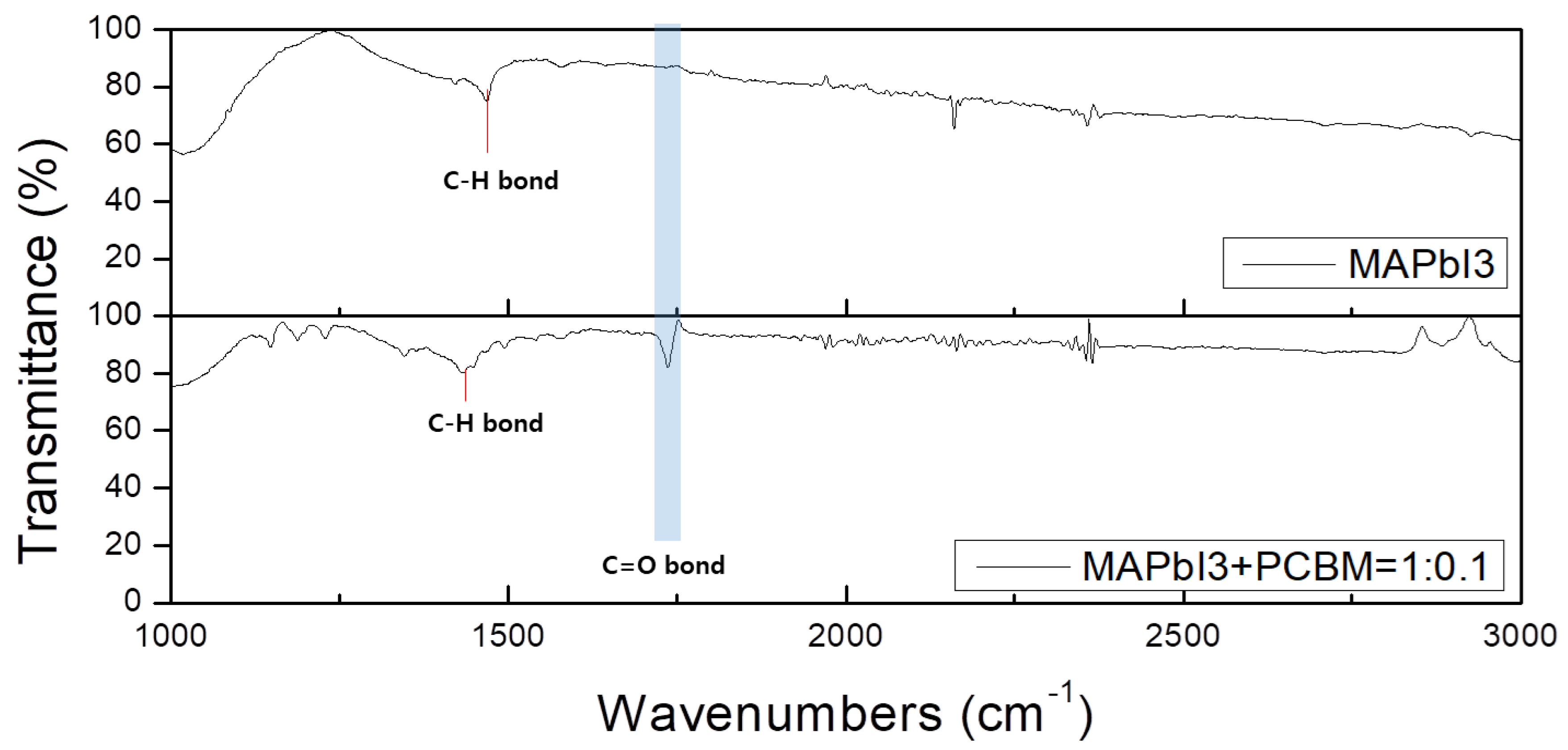
3.1. Crystal Structure and FTIR Spectra of Phenyl-C61-Butyric Acid Methyl Ester– Methyl Ammonium Lead Iodide (PCBM-MAPbI3) Hybrid Film

The HR-XRD data revealing the structural characteristics of the PCBM-MAPbI3 films with (made from 0.1:1 solution) and without PCBM are shown in Figure 2. The diffraction pattern of MAPbI3 exhibited peaks at 2θ = 13.97°, 28.15°, 40.63°, and 42.78°, corresponding to the (002), (004), (006), and (400) planes of the tetragonal crystal structure of perovskite, respectively [17,18]. As shown in Figure 2, the lattice diffraction peaks of the thin film based on the blend of MAPbI3 and PCBM were consistent with those of the pristine MAPbI3 film without PCBM. This indicates that the added fullerenes did not destroy the MAPbI3 crystal structures and had little effect on the MAPbI3 crystal structure. Supplementary Table S1 presents the grain size of the crystallites for the principal diffraction peak, which was calculated using the Scherrer equation [19]. The perovskite grain size of the PCBM-MAPbI3 hybrid film was comparable to that of the control MAPbI3 film without PCBM.
Figure 3 present FTIR spectra of the MAPbI3 film with and without PCBM. As shown in Figure 3, the FTIR spectra showed an observation of the stretching C = O vibration at 1750 cm-1 for the PCBM-MAPbI3 hybrid film. However, the stretching C = O vibrations of the control MAPbI3 film without PCBM could not observed. Therefore, elimination of their vibrations in FTIR spectra happened through complexation in the interface of C = O moiety with Pb atoms from perovskite, which is expected to reduce the charge recombination and increase the electron extraction in the MAPbI3-PCBM hybrid film [20].

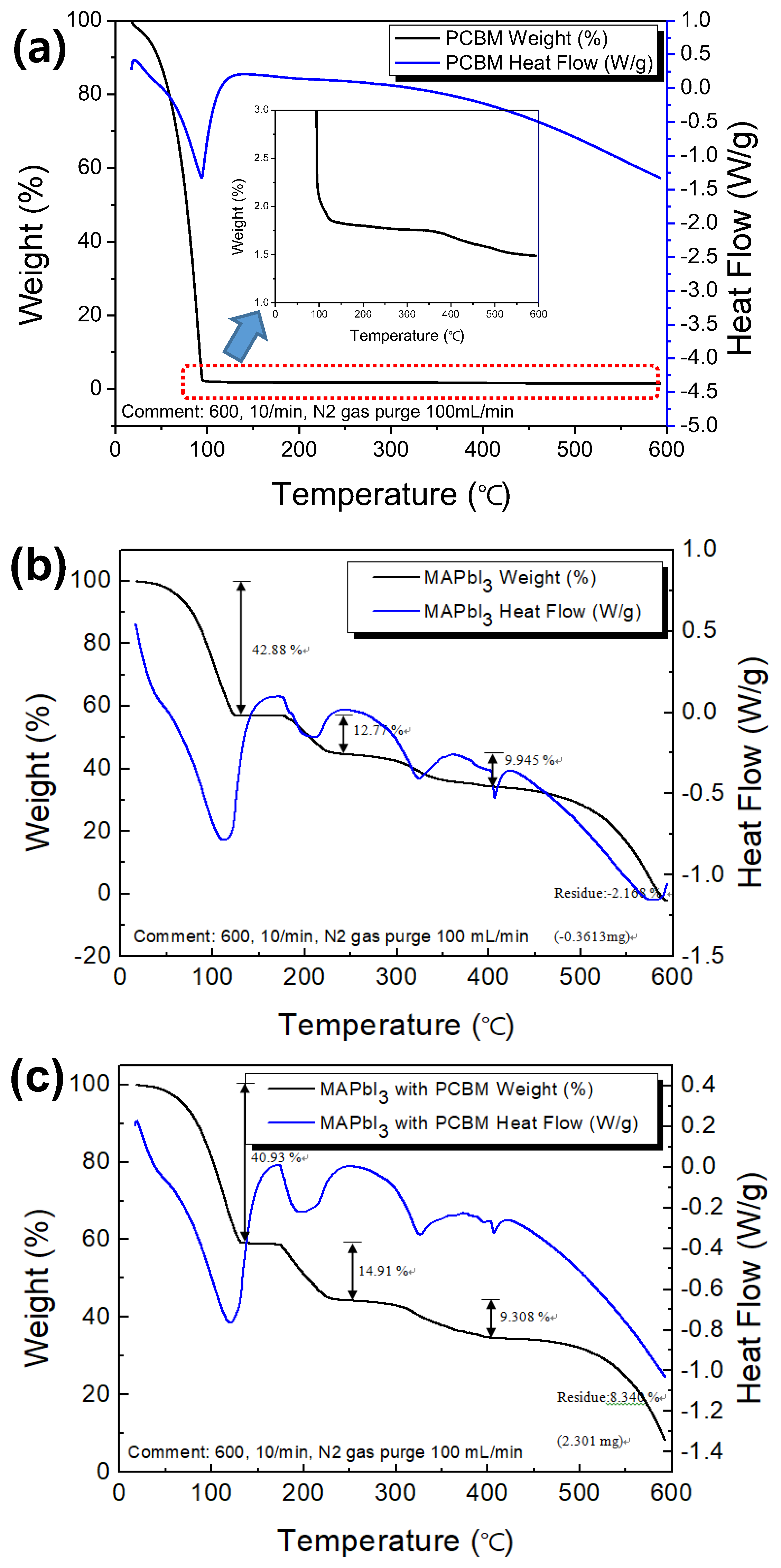
3.2. Thermal Behavior of MAPbI3, PCBM, and MAPbI3 with PCBM

The thermal properties of the PCBM solution, MAPbI3 precursor solution, and PCBM-MAPbI3 mixture solution were investigated via simultaneous TG-DTA measurements in a N2 atmosphere. From start to end, the weight-loss steps were delimited using the slope changes caused by thermal events in the DTA trace, which was recorded during the TG measurements. Figure 4a–c show the TG-DTA trace peaks recorded during the thermal degradation of PCBM, MAPbI3, and PCBM-MAPbI3, respectively. The inset in Figure 4a is enlarged data of the TG-DTA curve of PCBM in order to well distinguish data. From the TG-DTA plot shown in Figure 4a, two weight-loss steps were observed. The first and second steps were the CB solvent and PCBM, respectively. From these data, PCBM had thermal stability up to approximately 380 °C and then began to lose weight. In contrast, four weight-loss steps were observed in the case of the MAPbI3 precursor solutions with and without PCBM, as shown in Figure 4b,c. The first and second steps were the DMF solvent and DMSO weight-loss steps, respectively. As indicated by Figure 4b,c, in the third step, at approximately 400 °C, a weight-loss difference of approximately 0.6% was observed between the MAPbI3 precursor solutions with and without PCBM. In the final step, the MAPbI3 mixed with the PCBM solution had approximately 10% of its initial weight. This 10% remaining weight was due to the PCBM; thus, the PCBM-MAPbI3 (0.1:1 volume ratio) was well mixed.

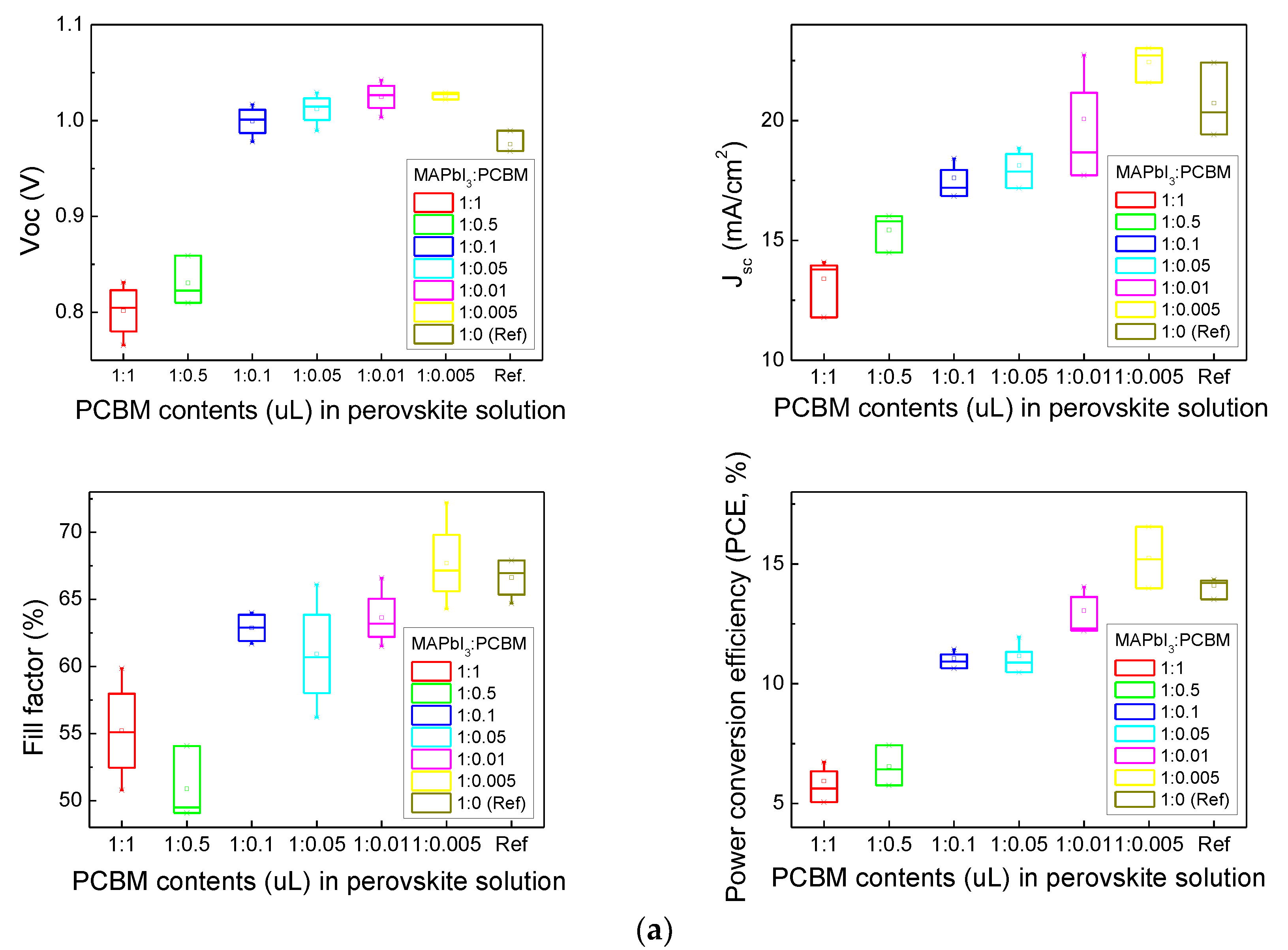
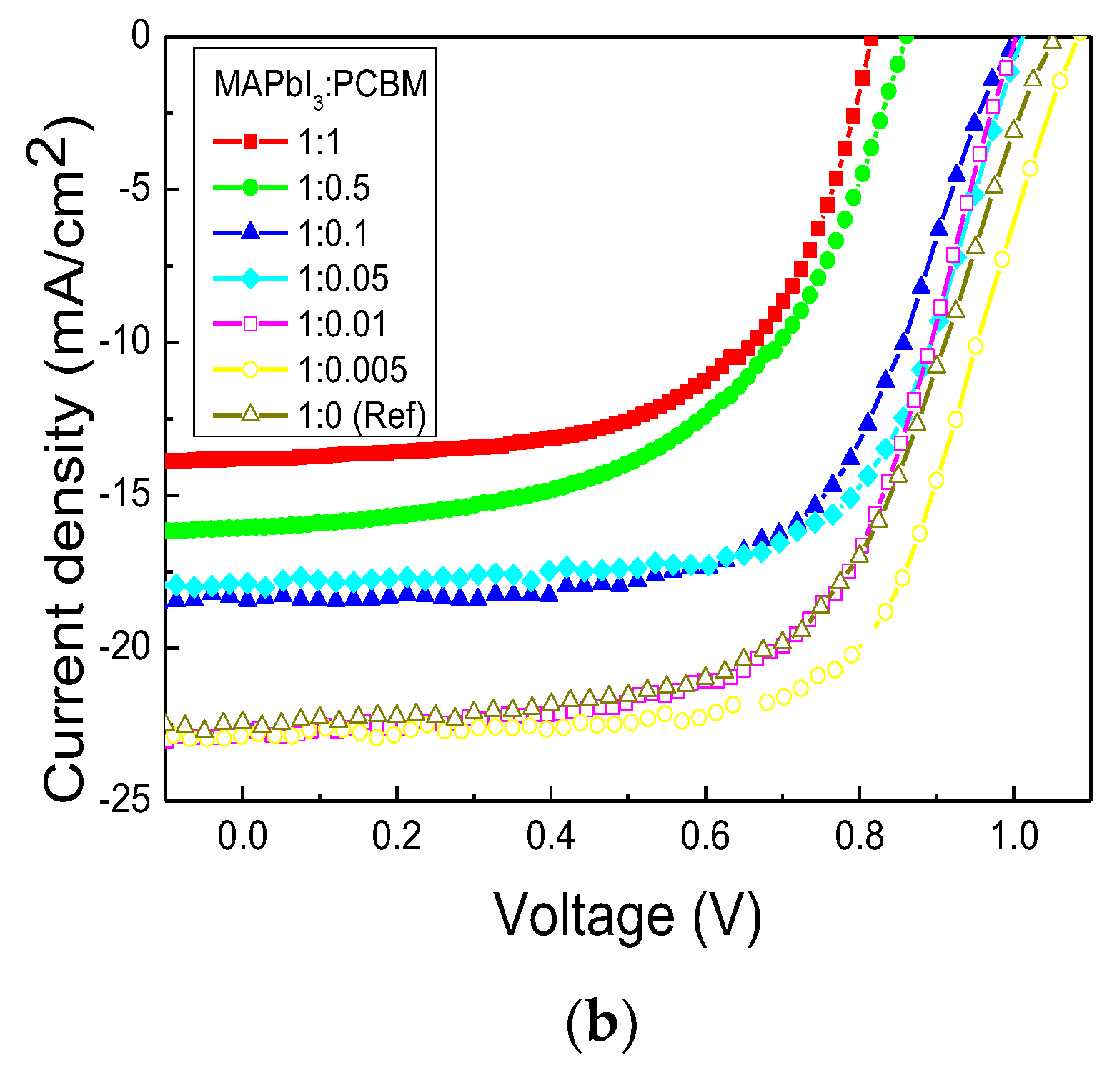
3.3. Photovoltaic Performance of Normal (n-i-p) Planar PSCs

Planar PSCs with a normal n-i-p structure (FTO/compact TiO2/MAPbI3 based absorber layer/Spiro-OMeTAD/Ag) were fabricated. The photovoltaic J–V characteristics of devices with different absorber layers are shown in Figure 5, and the corresponding device performance parameters are presented in Table 1. The different absorber layers were fabricated using MAPbI3 with different PCBM mixture ratios (in volume percent). As shown in Figure 5a, the device performance (short-circuit current density, open circuit voltage, fill factor, and efficiency) was highest when the PCBM-MAPbI3 mixture ratio was 0.005:1. When the PCBM mixture ratio was increased from 0.005:1 to 1:1, the device performance deteriorated. The best PSCs with a 0.005:1 mixture ratio exhibited improved device performance, with a short-circuit current density (Jsc) of 22.76 mA/cm2, an open-circuit voltage (Voc) of 1.0089 V, a fill factor (FF) of 72.2%, and an efficiency of 16.55%. This efficiency was significantly higher than that of 14.34% for pure MAPbI3 (0:1). Additionally, the device with the 0.005:1 PCBM-MAPbI3 mixed absorber layer had higher device performance than that with PCBM as the ETL layer (PCBM/MAPbI3/Spiro-OMeTAD structure), as shown in Supplementary Figure S2. Thus, introduction of PCBM into the MAPbI3 perovskite precursor enhanced the photovoltaic performance of the PSCs. We attributed the increased Jsc in the presence of a small amount of PCBM to the improved electron transport, and we attributed the increased FF to the improved film quality. Therefore, it was considered that when the fullerene derivative PCBM was blended into the perovskite precursor, the PCBM dispersed into the perovskite precursor passivated defects during perovskite self-assembly, improving the quality of the photoactive layer by filling pinholes and vacancies between perovskite grains [17]. To verify the impact of the PCBM on the perovskite materials, PCBM with different concentrations were blended into the precursor solution. At PCBM concentrations higher than 0.005:1, the solar-cell performance was degraded, and the number of dissolved fullerenes affected the overall performance of the PSCs. Experimentally, we can conclude that perovskite coating with the PCBM-MAPbI3 hybrid solution is essential for obtaining perovskite absorbers with characteristics suitable for planar-type solution-processed PSCs. The proposed method is very simple with regard to the precursor preparation and processing steps, and adding a small amount of PCBM to the perovskite solution can improve the device efficiency by 16.55%. It can be widely used for low-temperature and solution-processed planar PSC technology.

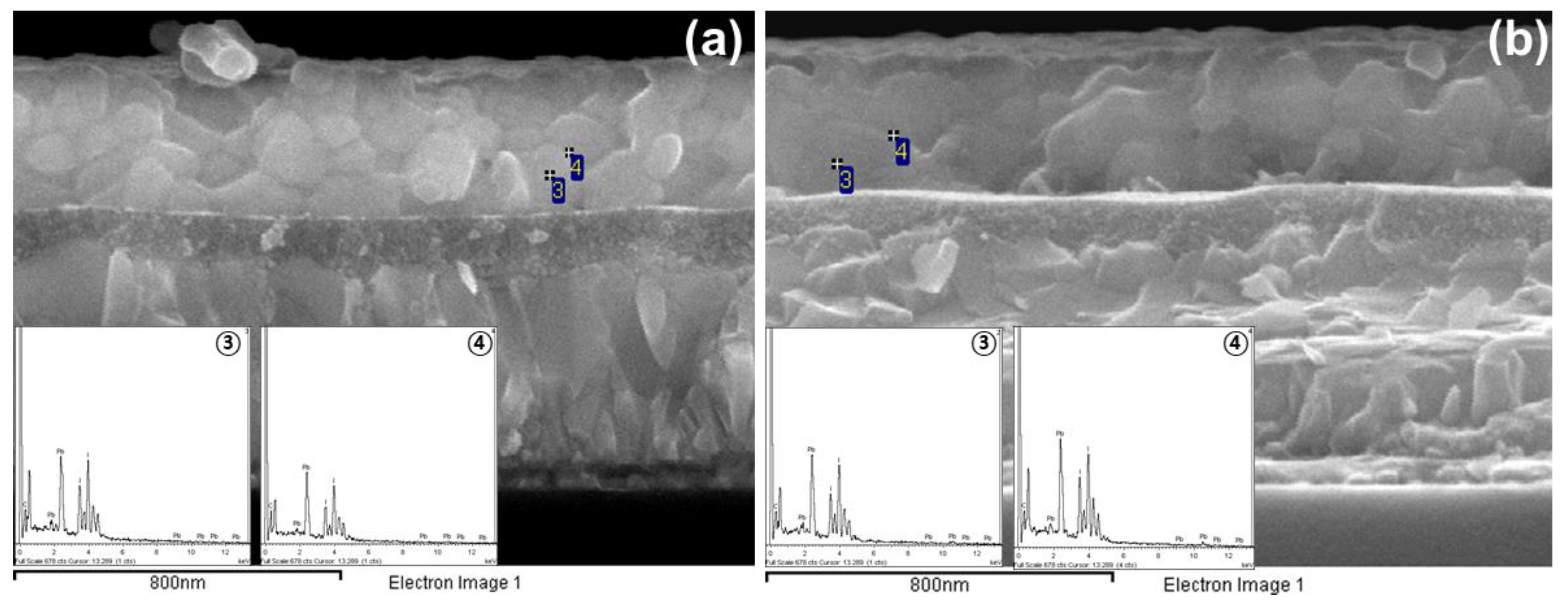
3.4. Difference in C Content Between Grain Interior and Grain Boundaries

As mentioned above and in reference [17], improved device performance is attributed to the PCBM passivation at the grain boundaries of the MAPbI3 film. To determine whether PCBM existed in grain boundaries of MAPbI3, we measured the PCBM distribution in the MAPbI3 films using scanning electron microscopy (SEM)-EDS mapping, as shown in Figure 6. The cross-sectional SEM images in Figure 6a,b show the microstructure of the MAPbI3 films with and without PCBM on the TiO2 ETL, respectively. The insets in Figure 6a,b present the EDS spectra for each point (3: grain interior; 4: grain boundary) shown in the SEM photograph. We attempted to determine the weight percent (wt%) of C using EDS mapping because it is difficult to measure the PCBM directly. The PCBM is a C-based fullerene derivative material (C72H14O2) comprising organic components. We observed a difference between the intra-grain and grain boundary C contents, as shown in Table 2. For the perovskite fabricated with the PCBM-MAPbI3 (0.005:1) hybrid solution, there was a large difference in the C content (+2.54 wt%) between the grain interior and grain boundary. For the perovskite fabricated with only the MAPbI3 solution, the difference (–3.22 wt%) was smaller. The C content of the PCBM-MAPbI3 (0.005:1) film was higher than that of the MAPbI3 film (for both the grain interior and the grain boundary). The experimental results confirm that PCBM was suggested to be preferentially located at the perovskite grain boundaries [17,21].

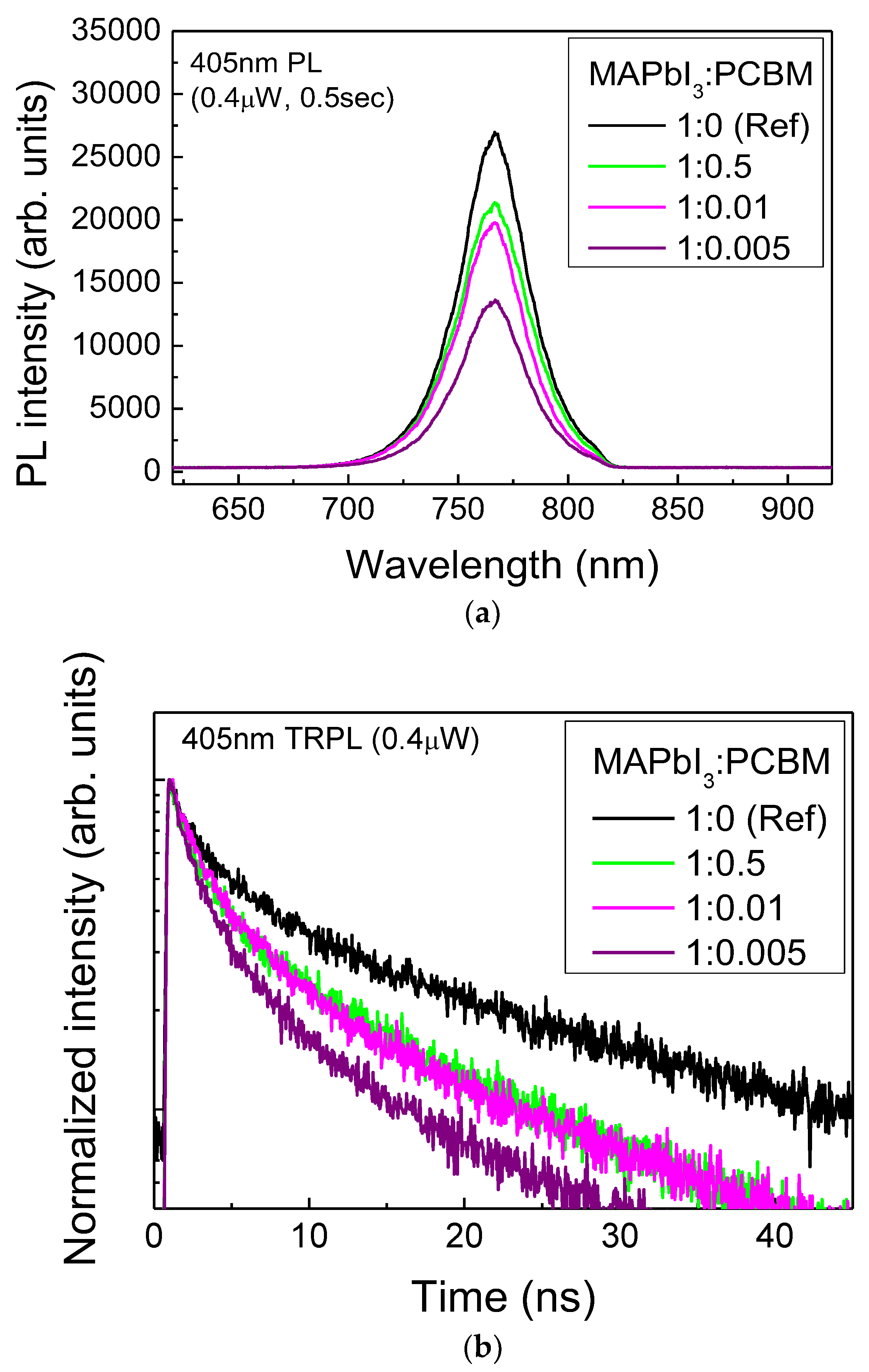
3.5. Steady-State and TRPL Decay

In order to further investigate the origin of the enhanced photovoltaic performance of PSCs using the PCBM-MAPbI3 hybrid film, we performed steady-state PL and TRPL measurements for elucidating the charge-extraction phenomena of the added PCBM in the mixed perovskite layers and the charge-transfer kinetics between the MAPbI3 films and the transport layers, respectively. Figure 7a shows the steady-state PL spectra of only MAPbI3 and PCBM-MAPBI3 hybrid films on glass substrates. As shown in Figure 7a, a significant PL quenching effect was observed when the perovskite layer formed with PCBM, indicating an efficient charge-transfer process at the perovskite layer [17,22]. In addition, the PL intensity of the perovskite was significantly reduced depending on the PCBM-MAPbI3 mixing ratio, which implies the difference charge transfer of MAPbI3 film depending on the PCBM ratio. As mentioned above from EDS results, it can be assumed that the added PCBM is filled with grain boundaries in the MAPbI3 film, producing continuous pathways for electron extraction. Figure 7b shows TRPL data measured by monitoring the peak emission at 767 nm. The corresponding lifetime of the TRPL decay curve fitted to a quadratic-exponential function [23] is presented in Table 3. Fitting the data with a bi-exponential decay function yielded two carrier lifetimes, indicating that the PL decay of perovskite occurred through two relaxation pathways: fast and slow decay processes. The fast and slow decays were attributed to PL quenching in the perovskite films through charge-carrier transfer at the interface and radiative decay, respectively [11]. For the MAPbI3 perovskite film without PCBM, a PL lifetime as long as 14.64 ns was observed. This long lifetime is essential for large exciton/carrier diffusion lengths to allow large film thicknesses for light harvesting [14]. When PCBM-MAPbI3 was mixed, rapid decay of lifetime was observed. The fast decay for the lifetime, which indicates that most of the electrons were efficiently delivered to the PCBM, suggests that the PCBM-MAPbI3 mixed layer induced rapid carrier extraction. The lifetime depending on the mixture ratio of PCBM indicated increased fullerene–MAPbI3 interfaces and facilitated more efficient electron extraction from the perovskite, which contributed to stronger fluorescence quenching and accelerated PL decay. Therefore, by dissolving the added PCBM in the MAPbI3 solution, both the electron-extraction and electron-transport abilities were significantly enhanced, leading to a far shorter lifetime. Thus, the formed layers had charge-extraction properties, which are beneficial for photovoltaic applications. Additionally, the results suggest that the incorporation of PCBM in MAPbI3 can improve the charge-carrier transfer efficiency at grain boundaries, which can suppress the charge-carrier recombination and increase the performance of the photovoltaic device.

4. Conclusions

PCBM-MAPbI3 hybrid solutions with various concentrations of PCBM were prepared. This PCBM-MAPbI3 hybrid mixing technique offered recombination inhibition because of the reduction of vacancies in the grain interior and the recombination center at the grain boundaries for spin-coated MAPbI3 films. TiO2-based planar PSCs fabricated using the PCBM-MAPbI3 hybrid solution exhibited an enhanced efficiency. The PCBM content was low, and the PCBM was able to passivate defects at the grain boundaries of MAPbI3. A champion efficiency of 16.55% was obtained in PSCs of the n-i-p normal planar device prepared using PCBM-MAPbI3 with a 0.005:1 mixture ratio. The proposed hybrid mixing technique with a PCBM additive can facilitate the fabrication of planar perovskite devices with enhanced PV performances.

Supplementary Materials

The following are available online at https://www.mdpi.com/2071-1050/11/14/3867/s1, Figure S1: Figure S1. Photograph of the MAPbI3 precursor solution. The mixed materials made using solutions with various PCBM additive concentrations (5, 10, 50, 100, 500, and 1000 μL) and a 1000-μL MAPbI3 solution are presented in this figure. As shown in this figure, the pristine PCBM-MAPbI3 precursor (0:1) solution exhibited a bright yellow color, and its color changed to dark brown with an increase in the PCBM concentration from 0.005 to 1. Figure S2. J–V characteristics of the FTO/PCBM/MAPbI3/Spiro-OMeTAD/Au solar cells. Table S1. Grain sizes (unit: Å) of the perovskite films.

Author Contributions

Conceptualization, M.K. (MiJoung Kim) and J.Y.; formal analysis, M.K. (MoonHoe Kim), J.O., and N.K.; project administration, J.Y., Y.K.; writing—original draft, M.K. (MiJoung Kim).

Funding

This research was supported by the Basic Science Research Program through the National Research Foundation of Korea (NRF) funded by the Ministry of Science, ICT & Future Planning (NRF-2019R1A2C4070248). This work was supported by the Korea Institute of Energy Technology Evaluation and Planning (KETEP) and the Ministry of Trade, Industy &Energy (MOTIE) of the Republic of Korea (No. 20163010012570). This work was also supported by the KU-KIST Graduate School Project.

Conflicts of Interest

The authors declare no conflict of interest.

References

  1. Tonui, P.; Oseni, S.O.; Sharm, G.; Yan, Q.; Mola, G.T. Perovskites photovoltaic solar cells: An overview of current status. Renew. Sust. Energ. Rev. 2018, 91, 1025–1044. [Google Scholar] [CrossRef]
  2. Fang, F.; Chen, J.; Wu, G.; Chen, H. Highly efficient perovskite solar cells fabricated by simplified one-step deposition method with non-halogenated anti-solvents. Org. Electron. 2018, 59, 330–336. [Google Scholar] [CrossRef]
  3. Cao, W.; Xue, J. Recent progress in organic photovoltaics: Device architecture and optical design. Energy Environ. Sci. 2014, 7, 2123–2144. [Google Scholar] [CrossRef]
  4. Noh, J.H.; Im, S.H.; Heo, J.H.; Mandal, T.N.; Seok, S.I. Chemical management for colorful, efficient, and stable inorganic-organic hybrid nanostructured solar cells. Nano Lett. 2013, 13, 1764–1769. [Google Scholar] [CrossRef] [PubMed]
  5. D’Innocenzo, V.; Grancini, G.; Alcocer, M.J.; Kandada, A.R.; Stranks, S.D.; Lee, M.M.; Lanzani, G.; Snaith, H.J.; Petrozza, A. Excitons versus free charges in organo-lead trihalide perovskites. Nat. Commun. 2014, 5, 3586. [Google Scholar] [CrossRef]
  6. Wehrenfennig, C.; Eperon, G.E.; Johnston, M.B.; Snaith, H.J.; Herz, L.M. High charge carrier mobilities and lifetimes in organolead trihalide perovskites. Adv. Mater. 2014, 26, 1584–1589. [Google Scholar] [CrossRef] [PubMed]
  7. Lv, Y.; Si, D.; Song, X.; Wang, K.; Wang, S.; Zhao, Z.; Hao, C.; Wei, L.; Shi, Y. Pseudo halogen-based 2D perovskite: A more complex thermal degradation mechanism than 3D perovskite. Inorg. Chem. 2018, 57, 2045–2050. [Google Scholar] [CrossRef]
  8. Liu, D.B.; Wang, G.; Wu, F.; Wu, R.; Chen, T.; Ding, B.F.; Song, Q.L. Crystallization process of perovskite modified by adding lead acetate in precursor solution for better morphology and higher device efficiency. Org. Electron. 2017, 43, 189–195. [Google Scholar] [CrossRef]
  9. Zeng, X.; Zhou, T.; Leng, C.; Zang, Z.; Wang, M.; Hu, W.; Tang, X.; Lu, S.; Fang, L.; Zhou, M. Performance improvement of perovskite solar cells by employing a CdSe quantum dot/PCBM composite as an electron transport layer. J. Mater. Chem. A 2017, 5, 17499–17505. [Google Scholar] [CrossRef]
  10. Li, F.; Ma, C.; Wang, H.; Hu, W.; Yu, W.; Sheikh, A.D.; Wu, T. Ambipolar solution-processed hybrid perovskite phototransistors. Nat. Commun. 2015, 6, 8238. [Google Scholar] [CrossRef] [Green Version]
  11. Wu, Y.; Yang, X.; Chen, W.; Yue, Y.; Cai, M.; Xie, F.; Bi, E.; Islam, A.; Han, L. Perovskite solar cells with 18.21% efficiency and area over 1 cm2 fabricated by heterojunction engineering. Nat. Energy 2016, 1, 16148. [Google Scholar] [CrossRef]
  12. Rafael, S.T.; Jorge, P.; Inés, G.B.; Silvia, C.; Ivet, K.; Ramón, T.Z.; Nazario, M.; Juan, L.D. Modified fullerenes for efficient electron transport layer-free perovskite/fullerene blend-based solar cells. ChemSusChem 2017, 10, 2023–2029. [Google Scholar]
  13. Silvia, C.; Michael, S.; Wolfgang, R.T.; Philippe, J.H.; Sebastian, F.W.; Konrad, D.; Silver, H.T.-C.; Amita, U.; Shaik, M.Z.; Anders, H.; et al. Poly(ethylene glycol)–[60]Fullerene-based materials for perovskite solar cells with improved moisture resistance and reduced hysteresis. ChemSusChem 2018, 11, 1032–1039. [Google Scholar]
  14. Shao, Y.; Xiao, Z.; Bi, C.; Yuan, Y.; Huang, J. Origin and elimination of photocurrent hysteresis by fullerene passivation in CH3NH3PbI3 planar heterojunction solar cells. Nat. Commun. 2014, 5, 5784. [Google Scholar] [CrossRef] [PubMed]
  15. Ahn, N.Y.; Son, D.Y.; Jang, I.H.; Kang, S.M.; Choi, M.S.; Park, N.G. Highly reproducible perovskite solar cells with average efficiency of 18.3% and best efficiency of 19.7% fabricated via Lewis base adduct of lead(II) iodide. JACS 2015, 137, 8696–8699. [Google Scholar] [CrossRef]
  16. Son, D.Y.; Lee, J.W.; Choi, Y.J.; Jang, I.H.; Lee, S.H.; Yoo, P.J.; Shin, H.J.; Ahn, N.Y.; Choi, M.S.; Kim, D.H.; et al. Self-formed grain boundary healing layer for highly efficient CH3NH3PbI3 perovskite solar cells. Nat. Energy 2016, 1, 16081. [Google Scholar] [CrossRef]
  17. Xu, J.; Buin, A.; Ip, A.H.; Li, W.; Voznyy, O.; Comin, R.; Yuan, M.; Jeon, S.; Ning, Z.; McDowell, J.J.; et al. Perovskite–fullerene hybrid materials suppress hysteresis in planar diodes. Nat. Commun. 2015, 6, 7081. [Google Scholar] [CrossRef]
  18. Luo, S.; Daoud, W.A.; Luo. Crystal structure formation of CH3NH3PbI3-xClx perovskite. Materials 2016, 9, 123. [Google Scholar] [CrossRef]
  19. Cullity, B.D.; Stock, S.R. Elements of X-Ray Diffraction, 3rd ed.; Prentice-Hall Inc.: Upper Saddle River, NJ, USA, 2001; pp. 167–171. ISBN 0-201-61091-4. [Google Scholar]
  20. Tian, C.; Castro, E.; Wang, T.; German, B.S.; Gloria, R.; Luis, E. Improved performance and stability of inverted planar perovskite solar cells using fulleropyrrolidine Layers. ACS Appl. Mater. Interfaces 2016, 8, 31426–31432. [Google Scholar] [CrossRef]
  21. Jorge, P.; Juan, L.D.; Ramόn, T.Z. Physicochemical phenomena and application in solar cells of perovskite:fullerene films. J. Phys. Chem. Lett. 2018, 9, 2893–2902. [Google Scholar]
  22. Liu, X.; Huang, P.; Dong, Q.; Wang, Z.; Zhang, K.; Yu, H.; Lei, M.; Zhou, Y.; Song, B.; Li, Y. Enhancement of the efficiency and stability of planar p-i-n perovskite solar cells via incorporation of an amine-modified fullerene derivative as a cathode buffer layer. Sci. China Chem. 2016, 60, 136–143. [Google Scholar] [CrossRef]
  23. Redinger, A.; Levcenko, S.; Hages, C.J.; Greiner, D.; Kaufmann, C.A.; Unold, T. Time resolved photoluminescence on Cu(In, Ga)Se2 absorbers: Distinguishing degradation and trap states. Appl. Phys. Lett. 2017, 110, 122104. [Google Scholar] [CrossRef]
Figure 1. Schematic of the n-i-p normal device architecture of this study. MAPbI3, methyl ammonium lead iodide; PCBM, phenyl-C61-butyric acid methyl ester; ETL, electron transport layer; HTL, hole transport layer; and FTO, fluorine-doped tin oxide.
Sustainability 11 03867 g001
Figure 2. XRD patterns of films prepared from MAPbI3 and MAPbI3 mixed with PCBM (0.1:1 mixture ratio: 100 μL of PCBM mixed with 1000 μL of MAPbI3 solution).
Sustainability 11 03867 g002
Figure 3. FTIR spectra for MAPbI3 and PCBM-MAPbI3 hybrid films.
Sustainability 11 03867 g003
Figure 4. TG-DTA data for (a) PCBM, (b) MAPbI3, and (c) the PCBM-MAPbI3 hybrid solution in a N2 atmosphere.
Sustainability 11 03867 g004
Figure 5. (a) Photovoltaic properties of MAPbI3 perovskite solar cells (Voc, Jsc, FF, and efficiency) prepared with MAPbI3 only and with different PCBM-MAPbI3 mixture ratios; (b) J–V characteristics of the MAPbI3 PSCs prepared with MAPbI3 only and the PCBM-MAPbI3 hybrid solutions of different mixture ratios.
Sustainability 11 03867 g005aSustainability 11 03867 g005b
Figure 6. Cross-sectional SEM images showing the microstructure of the MAPbI3 films (a) with and (b) without PCBM on the TiO2 ETL. The insets in (a,b) present EDS spectra for each point (3: grain interior; 4: grain boundary).
Sustainability 11 03867 g006
Figure 7. (a) Steady-state photoluminescence (PL) of films prepared from MAPbI3 and MAPbI3 mixed with PCBM; (b) time-resolved photoluminescence (TRPL) spectra of corresponding films prepared from MAPbI3 and MAPbI3 mixed with PCBM.
Sustainability 11 03867 g007
Table 1. Device current-voltage characteristics at various PCBM ratios.
StructureMAPbI3:PCBM Ratio (volume %)Jsc (mA/cm2)Voc (V)FF (%)Efficiency (%)
FTO/TiO2/PCBM-MAPbI3/Spiro-OMeTAD/Au1:113.790.815059.856.73
1:0.516.010.859154.077.43
1:0.117.371.00661.711.43
1:0.0517.871.01266.111.95
1:0.0122.741.003261.514.04
1:0.00522.761.008972.216.55
FTO/TiO2/MAPbI3/Spiro-OMeTAD/Au1:0 (Ref)21.820.968367.914.34
Table 2. Elemental composition measured using EDS.
SamplesMAPBI3:PCBM = 1:0.005Only MAPbI3
ElementIntra-Grain (wt%)Grain Boundary (wt%)DifferenceIntra-Grain (wt%)Grain Boundary (wt%)Difference
C K21.2923.83+2.5420.7517.53–3.22
I L48.4844.69+3.7948.7250.61+1.89
Pb M30.2331.48+1.2530.5331.87+1.34
Totals100.00100.00 100.00100.00
Table 3. Comparison of the lifetimes at various PCBM ratios.
1:0.51:0.011:0.0051:0 (Ref)
A10.442760.413950.372350.70634
t113.1806312.461410.117541.96384
A20.944740.931561.16080.48923
t21.677032.063181.6243216.78579
τ10.724391519.638790197.28458590814.64394564

