Abstract
In order to achieve DC voltage matching, on-board charging, and DC/AC power inversion, three independent power converters are often needed in traditional Distributed Power Converter (DPC) systems of electric vehicles (EVs): bidirectional DC/DC (Bi-DC/DC), AC/DC, and DC/AC. The requirement of electronic devices such as power switches, inductors, and capacitors make the converter costly and complicated in structure. In this paper, a power converter with multi-operating mode (PCMM) is presented. The proposed PCMM can work in Bi-DC/DC, AC/DC, and DC/AC modes. The state-space averaging model of PCMM considering resistance of Insulated Gate Bipolar Transistor (IGBT) and the inductor is presented. Based on this model, the transfer function of the system is derived and the controller is designed. The simulation and experimental results show that PCMM can meet the design target and verify the feasibility of the model. The measurement results show that the weight of PCMM proposed in this paper is reduced by 51.2% compared with the traditional structure.
1. Introduction
Carbon dioxide (CO2) from vehicle exhaust is one of the main causes of the greenhouse effect. Electric vehicles (EVs) are considered to be an important development direction of the future automobile industry because of their advantages in reducing CO2 emissions. In order to improve the performance of the energy storage system, a hybrid energy source can be used. [1]. In electric vehicles (EVs), lithium-ion batteries or fuel cells are often used as the primary power source, which is supplemented by a super-capacitor pack or battery pack as the auxiliary power source to constitute a hybrid energy storage system (HESS) [2]. As the primary and auxiliary power sources usually have different voltage levels, a DC/DC converter is needed to achieve voltage matching [3]. Meanwhile, in order to charge the battery pack, a charger with AC/DC function is needed [4], which converts the grid AC into DC. In addition, when AC power supply is required for cases like outdoor activities, a DC/AC inverter is needed to convert the battery DC into AC [5]. Simultaneously, a DC/AC inverter also needs to have the grid connection function, so that the battery power level of EVs can be fed back to the grid after inversion when the EVs sits idle in the garage, thereby playing a role in grid peak shifting and regulation.
The DC/DC converter plays an important role in DC power level conversion of energy storage systems, including hybrid energy storage systems [6], PV systems [7,8], fuel cell systems [9], etc. Interleaved is one of the DC/DC topologies [9]. The advantages of this topology include low output current ripple and high power density [10]. The interleaved DC/DC can be composed of two phases [11], three phases [12], or multi-phase [13]. It has greatly reduced volume and weight compared to the traditional Bi-DC/DC.
To improve the power factor in the process of AC/DC conversion, power factor correction (PFC) is needed with a special circuit. The traditional PFC method adds a boost converter behind the rectifier bridge [14]. Such a method requires a rectifier bridge and a boost circuit, which has the disadvantage of low conversion efficiency. To improve the conversion efficiency, researchers have proposed a bridgeless PFC circuit topology that does not require rectifier bridges [15]. One solution is to add two additional diodes to improve the EMI problem [16]. Another solution is bridgeless PFC with totem pole topology [17]. This topology does not require additional power elements. It only needs to drive two switches of the bridge independently.
There are three main topologies for DC/AC inverters [18]. One is the push-pull configuration inverter, which consists of few power devices and is easy to drive [19]. However, due to structural characteristics of the circuit itself, the push-pull circuit topology cannot output sinusoidal voltage waveforms, which is suitable for low-power applications. Another is the half-bridge topology inverter, which has few switching components and a simple structure. Nevertheless, the rated current of its power switch is twice that of the power components in a full-bridge inverter circuit, with large current stress. The third one is the full-bridge inverter, whose output current and current through switching components are both half of the half-bridge inverter circuit. The drive circuit of the full-bridge inverter is more complex than the two previous topologies due to the presence of four switching devices.
In EVs with hybrid energy storage systems, the traditional Distributed Power Converter (DPC) scheme needs at least three independent Bi-DC/DC, AC/DC, and DC/AC converters. When an EV is being driven, the buck converter and boost converter are needed to convert the power between the battery pack and the auxiliary energy. An AC/DC converter is needed to charge the battery pack. A DC/AC converter is needed to supply the AC power to the electric appliances. The topology of this system is shown in Figure 1. Each converter needs to be equipped with separate radiators, which are thus structurally complex and costly.
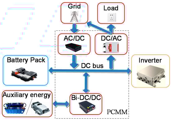
Figure 1.
Conventional distributed power converter (DPC) topology.
Some researchers have studied multifunctional power converters. The power converter system integrating a motor controller and battery charger proposed by JY Lee et al. enabled the AC/DC conversion to share the power devices of a motor controller [20]. Serkan Dusmez et al. integrated the AC/DC charger of a battery on the basis of a DC/DC converter by sharing the power devices of a boost DC/DC converter [21,22]. Ting-Chia Ou et al. proposed a multi-input power converter to achieve different operation modes [23].
Previous research on power converters mainly focuses on their performance. For the integration converters, the literature only mentioned DC/DC and AC/DC integration. Compared with the traditional converters, this paper presents a novel integrated multi-function converter include Bi-DC/DC, AC/DC, and DC/AC. Based on the topology of the Bi-DC/DC, the presented PCMM adds only one switch and an AC capacitor to achieve multifunction operation. It shares the inductor, capacitor, and IGBT modules and offers three conversions functions and reduced system weight.
This paper presents a PCMM converter and builds the model of the system using a state-space averaging modelling method [24]. Section 2 introduces the model of the converter in each operating mode. Part 3 performs the experimental results. Experimental evaluation of the PCMM is presented in Section 4.
2. Modelling and Control of the System
The PCMM proposed in this paper has three working modes. The topology is shown in Figure 2. When working in Bi-DC/DC mode, the switch K2 is turned on and the switch K1 is turned off. The system works in buck mode or boost mode. In AC/DC mode, switch K1 is turned on and the switch K2 is turned off, the system works with bridgeless PFC topology, and the energy flows from the grid to the battery side. In DC/AC mode, switch K1 is turned on and switch K2 is turned off. The energy flows from the battery side to the AC side to achieve DC to AC conversion.
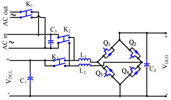
Figure 2.
Proposed topology.
As shown in Figure 3, when the vehicle is driving, the PCMM works in the Bi-DC/DC mode. The controller distributes the power for the battery and the auxiliary energy source according to the power demand of the inverter. The auxiliary energy source will provide energy when the PCMM operates in the boost mode. PCMM detects the DC bus voltage, calculates the reference current according to the power that the auxiliary energy needs to respond with. When the auxiliary energy source is needed for energy recovery, the PCMM operates in buck mode. The PCMM detects the voltage of the auxiliary energy and calculates the target current according to the power recovered by the auxiliary energy. When the battery pack needs charging, the PCMM operates in the AC/DC mode. In the constant current charging stage, the control objective of the PCMM is the output current. In the constant voltage charging stage, the control objective of PCMM is the output voltage. The PCMM works in DC/AC mode when it is necessary to provide single-phase AC for the electrical equipment. PCMM adopts double loop control; the current of the inductor is the inner loop, the output AC voltage is outer loop, and the control target is output voltage.
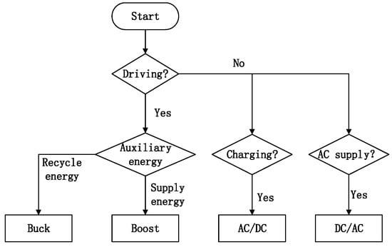
Figure 3.
Flow chart of the function needed in EVs with hybrid energy storage systems.
2.1. Bi-DC/DC Mode
In buck mode of the Bi-DC/DC converter, the equivalent circuit of the system is as show in Figure 4.
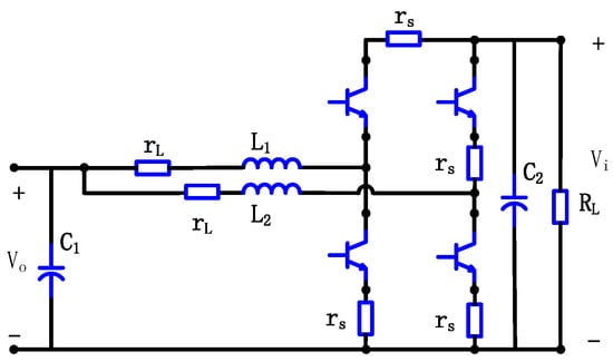
Figure 4.
The equivalent circuit of the Bi-DC/DC mode.
The voltage of the capacitor , the current of the inductors , and are selected as the state variable of the system. The high side voltage is selected as the input variable, and the low side voltage is selected as the output variable. The state equations and output equations of the system can be given as Equations (1) and (2).
For the bi-DC/DC converter operating in an inductor continuous mode (CCM), the coefficient matrix of the state space averaging equations is given as Equation (3).
where, is the internal resistance of inductor, is the internal resistance of the IGBT, and d is the duty cycle of the PWM.
In steady state, the derivative of each state variable is zero, and the relation between the steady state output voltage and the input voltage can be expressed by Equation (4).
where, RL is the load resistance.
The average vector of the system can be expressed as the sum of the steady-state value and the small signal value, shown in Equation (5).
In the vicinity of the steady state, the small signal model of the system can be obtained by the partial derivative of the variable, and the Laplace transform can be used as Equation (6).
Make , the transfer function of the input voltage to each state variable can be determined via Equation (7).
Make , the transfer function of the duty cycle to each state variable can be calculated as Equation (8).
The boost model and the buck model have dual symmetry, and the coefficient matrix of the average state space equation in the boost mode is given by Equation (9).
The relation between the steady state output voltage and the input voltage can be expressed as Equation (10).
The transfer function of the input voltage to each state variable can be determined by Equation (11).
The transfer function of the duty cycle to each state variable can be calculated with Equation (12).
The control structure of the Bi-DC/DC mode is shown in Figure 5. The controller consists of two inner loops and one outer loop. In buck mode, Vref is the reference voltage of the low voltage side, Vout is the output voltage, dx1 is the duty cycle of Q1, and dx2 is the duty cycle of Q2. In boost mode, Vref is the reference voltage of the high voltage side, Vout is the output voltage, dx1 is the duty cycle of Q3, and dx2 is the duty cycle of Q4. PIx1, PIx2, and PIx3 is the PI regulator of the system. Based on the model of the system illustrated in Equations (1)–(12), the parameters of the PI regulators in buck mode and boost mode can be obtained easily by the “sisotool” toolbox of MATLAB.
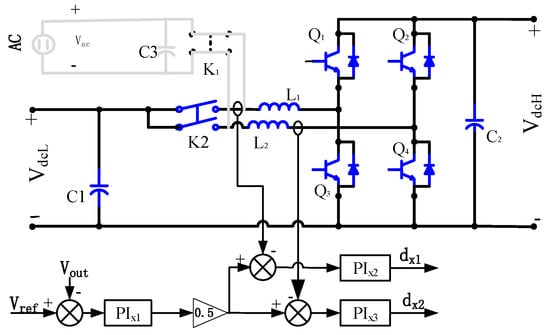
Figure 5.
The control structure of the Bi-DC/DC mode.
2.2. AC/DC Mode
The equivalent circuit of the AC/DC mode is show in Figure 6.
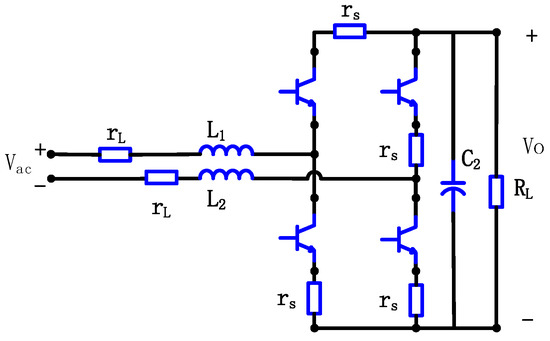
Figure 6.
The equivalent circuit of the AC/DC mode.
Referring to Figure 6, assume that the parameters of the four power switches are the same. The equivalent circuits of the negative half cycle and the positive half cycle of the sine wave are the same. Therefore, only the positive half cycle needs to be analyzed. The voltage of the capacitor , the current of the inductor , and are selected as the state variables of the system. The AC side voltage is selected as the input variable, and the high side voltage is selected as the output variable. The state space equation of the system and the output equation are expressed in Equations (1) and (2). The coefficient matrix of the average state space average equation of the system is expressed by Equation (13).
In steady state, the relation between the steady state output voltage and the input voltage can be expressed as Equation (14).
The average vector of the system can be expressed as the sum of the steady-state value and the small signal value, as shown in Equation (15).
In the vicinity of the steady state, the small signal model of the system can be obtained by the partial derivative of the variable, and the Laplace transform is carried out with Equation (16).
Make , the transfer function of the input voltage to each state variable can be determined as Equation (17).
Make , the transfer function of the duty cycle to each state variable can be calculated as Equation (18).
The control structure of the AC/DC mode is shown in Figure 7.
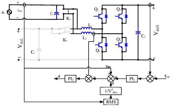
Figure 7.
The control structure of the AC/DC mode.
The loop is composed of an inner current loop and an outer loop. The output of the regulator PI1 in the outer loop and the input voltage are multiplied, so that the output current is proportional to the input voltage. In order to keep the output power constant when the input voltage is disturbance, the RMS value of the input voltage is added as the feed forward. The signal calculated by the multiplier is used as a reference of the current loop, and the current loop is adjusted by regulator PI2 to obtain the duty cycle of the PWM.
2.3. DC/AC Mode
The wave form of the output in DC/AC mode is a sinusoidal form, and there is no DC steady state operation point. It is a typical large signal nonlinear system, and the equivalent circuit in the DC/AC mode is shown in Figure 8.
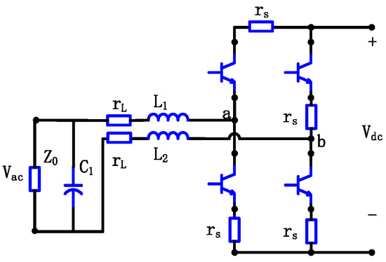
Figure 8.
The equivalent circuit in DC/AC mode.
The voltage of the capacitor and the current (, ) of the inductors (, ) are selected as the state variables of the system. The voltage between the two points ‘a’ and ‘b’ is taken as the input variable, and the output voltage is taken as the output variable. Because of , the equation of the circuit can be expressed as Equations (19)–(22).
The coefficient matrix of the state space equation is shown in Equation (23).
The voltage is a discontinuous signal, which can be averaged over a switching period to obtain its average state. For unipolar modulation, when the modulation wave is and the carrier amplitude is , the average value of the voltage in one period can be expressed as Equation (24).
Substituting Equation (24) into the state equation of the system, the related characteristics can be derived. The internal resistance of the two inductors is defined as , then the transfer function of the system can be expressed by Equation (25).
The control structure of the DC/AC mode is shown in Figure 9.
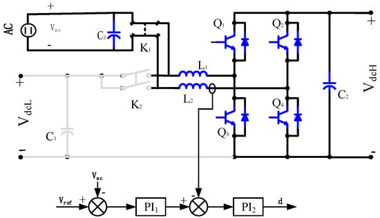
Figure 9.
The control structure of the DC/AC mode.
The control system is composed of an inner loop and an outer loop. The reference voltage () of the output voltage is a sinusoidal wave with required frequency. Regulating by the regulator (PI1), the reference of the current loop is obtained, and the duty cycle of the PWM is output by the regulator (PI2).
2.4. Limitations of Proposed Model
The PCMM model established in this paper has the following limitations.
Firstly, the model is based on the average state variable established by the average state space model. The state variable of the model reflects the average value of variables in a switching cycle. This model cannot effectively reflect the description of switch details.
Secondly, the model is a small signal model, which reflects the small signal disturbance characteristic of the system near steady state. When the system is disturbed by a large signal, such as start-up, short circuit, or sudden break, the system characteristics cannot be accurately described.
To reflect the system characteristics more accurately, a nonlinear modeling method is needed. However, the system model obtained by the nonlinear modeling method is rather complex, which will bring difficulties to the controller’s design. This model can use classical control theory to design a controller for PCMM. It can quickly design a controller that meets the engineering requirements.
3. Simulation of the PCMM
According to the design requirements of a certain vehicle model, the PCMM needs to achieve DC conversion between the super capacitor bank and the lithium-ion battery pack, conversion from single-phase AC to the lithium-ion battery pack, and conversion from the lithium-ion battery pack to single-phase AC. The performance requirements of the PCMM are shown in Table 1.

Table 1.
Design parameters of the power converter with multi-operating mode (PCMM).
In order to meet the requirements of current ripple and voltage ripple in different modes, capacitance and inductance need to be matched with PCMM design parameters [25]. The results obtained by the parameter matching show that the inductance of and is 690 uH, the AC filter capacitor is 3 μF, the high side filter capacitor is 9400 F, and the low side capacitor is 2200 F. Matlab/Simulink was used for simulation and the main circuit of the simulation model is shown in Figure 10.
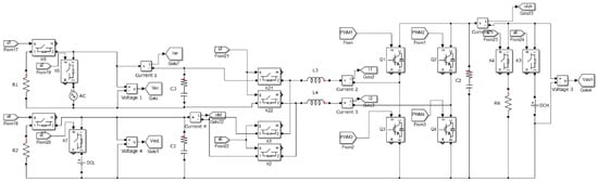
Figure 10.
Main circuit of the simulation model.
3.1. Bidirectional DC/DC Mode
In buck mode, as shown in Figure 11, the inductor current and drive signals are obtained for an input voltage of 350 V, output voltage of 220 V, and output power of 30 kW. During operation, the two IGBTs turn on alternately and each phase lags by 180 degrees to reduce the output current ripple. In Figure 11, IL1 and IL2 are the current waveform of the two inductors. IL is the sum of IL1 and IL2. The current ripple of IL1 is 55.0 A. Because of the interleaved structure, the output current IL is reduced to 23.8 A.
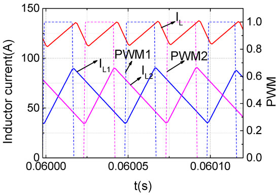
Figure 11.
Inductor current waveform in bi-directional DC/DC mode.
In boost mode, for the input voltage of 220 V, output voltage of 350 V, and load power of 30 kW, the output voltage response is as shown in Figure 12a.
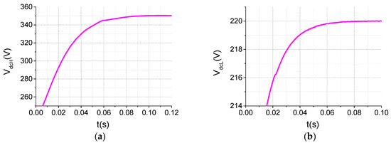
Figure 12.
Output voltage waveform: (a) boost mode; (b) buck mode.
In buck mode, for the input voltage of 350 V, output voltage of 220 V, and load power of 30 kW, the output voltage response process is as shown in Figure 12b.
The output voltage reached a steady state in 100 ms and 80 ms in boost mode and buck mode, respectively. The error of output voltage is less than 1%. The controller designed based on the presented model is accurate.
3.2. AC/DC Mode
In AC/DC mode, simulation studies were carried out for the input voltages of 180 V and 240 V, respectively. For the output voltage of DC 400 V, load resistance of 60 ohms, and output power of 2.667 kW at steady state, the input voltage and current are as shown in Figure 13. In this mode, the PCMM rectified the AC power supply and realized power factor correction.
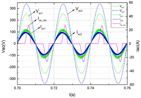
Figure 13.
Output voltage and current waveform.
As shown in Figure 13, Vac1 is the waveform for the input voltage RMS value of 180 V, and Iac1 is the input current waveform. Vac2 is the waveform for the input voltage RMS value of 240 V, and the is the corresponding input current waveform. In contrast, is the input current without power factor correction. With the power factor correction, the input current changes proportionally with the input voltage, and the circuit shows a resistive load characteristic. The power factor is greater than 0.996.
The spectrum of input current is analyzed, and different order harmonics are shown in Table 2. The total harmonic distortion (THD) of the input current (Ih1) is 6.62% for AC 180 V. For AC 240 V, the THD of the input current (Ih2) is 8.22%, which meets the requirements of the Class A equipment in the IEC6000-3-2 standard (Ihs). Ih_rec is the harmonic of the input current without power factor correction.
Table 2.
Harmonics of input current.
3.3. DC/AC Mode
In an independent inverter mode, the output AC voltage and current phase do not need to track the phase of the grid voltage. A voltage controller is used to regulate the output voltage. For the DC voltage of 400 V and output voltage RMS value of 220 V, the output voltage and current are shown in Figure 14.
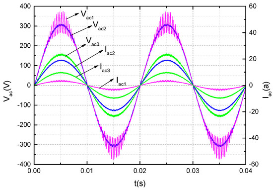
Figure 14.
Output voltage and current waveform.
For the output voltage of RMS 220 V with loads of 500 W, 3 kW, and 1.5 kW, the voltage , , and are shown in Figure 14. Iac1, Iac2, and Iac3 are the current waveforms for 500 W, 3 kW, and 1.5 kW operation.
The output current is analyzed by frequency spectrum, and each order harmonic is shown in the Table 3. Ih1, Ih2, and Ih3 are the harmonics of Iac1, Iac2, and Iac3, respectively. The THD of the input current is 9.12% in 500 W, 1.53% in 3 kW (220 V), and 2.28% in 1.5 kW (110 V) mode, respectively. It can meet the requirements of Class A equipment according to the IEC6000-3-2 standard.
Table 3.
Harmonics of output current.
4. Experimental
In order to reduce the inductor volume, the L1, L2 is 69 uH/150 A. In AC/DC and DC/AC modes, L1 and L2 are connected in series with an inductor for the values of 1.2 mH/20 A. Filter capacitor C3 employs a 3 uF/600 V capacitor, filter capacitor C2 employs two 4700 F/500 V aluminum electrolytic capacitors, and filter capacitor C1 employs a 2200 F/400 V aluminum electrolytic capacitor. The four switch tubes are made up of two MITSUBISHI PM200DV1A120 IPM modules. The current is sampled by a HAS-200-s LEM current sensor. The voltage sensor uses LEM’s LV25-P voltage sensor to isolate the samples. The experimental test bench is shown in Figure 15.
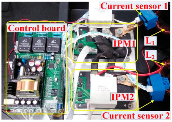
Figure 15.
Experimental test bench.
According to actual measurements of the experimental prototype, the electronic components weigh 8.7 kg, while accessories, such as the enclosure and wires, weigh 7.4 kg, resulting in a total prototype weight of 16.1 kg. If the Bi-DC/DC, DC/AC, and AC/DC converters are installed independently, the total weight will be 33 kg. Comparatively, PCMM can reduce the weight by 51.2%.
4.1. Bi-DC/DC Mode
The input voltage and the output voltage in Bi-DC/DC model are shown in Figure 16a,b. In the figures, the pink curves are the high side voltage. The blue curves are the low side voltage.
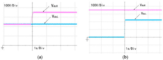
Figure 16.
Input voltage and output voltage in (a) boost mode, (b) buck mode.
In boost mode, for an input voltage of 220 V, output voltage of 350 V, and load resistance of 30 Ω, the input voltage and the output voltage are as shown in Figure 16a during initiation of conversion. The conversion efficiency reaches 96.4%.
In buck mode, for an input voltage of 350 V, output voltage of 220 V, and load resistance of 30 Ω, the input voltage and output voltage are as shown in Figure 16b during initiation of conversion. The conversion efficiency is 96.1%.
4.2. AC/DC Mode
The AC voltage connects a 3 kVA transformer to adjust the grid voltage for input of PCMM. The DC output is connected to a resistance load. In the absence of power factor correction, the four reverse diodes form a rectifier bridge, and the circuit operates in the uncontrolled rectifier state. The input voltage and current of the AC side are shown in Figure 17a. The power factor is 0.57, and the output voltage is uncontrollable.
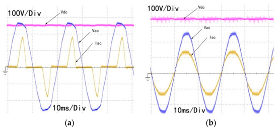
Figure 17.
Voltage and current in AC/DC mode: (a) without power factor correction; (b) with power factor correction.
With power factor correction, for an output voltage of DC 350 V, the input current is proportional to the input voltage. The input voltage, input current, and output DC voltage are shown in Figure 17b. By power factor correction, the power factor is increased to 0.988. The conversion efficiency is 96.4%, the is 5.68%, and the output voltage is stable under the regulation of the regulator.
4.3. DC/AC Mode
In DC/AC mode, for an input voltage of DC 350 V, output voltage of RMS 220 V, load resistance of 54 Ω, and frequency of 50 Hz, the wave form of the output voltage, input current, and DC side voltage are as shown in Figure 18a. The pink curve is the DC high side voltage, the blue curve is the output voltage, and the yellow curve is the output current. The THD of the output current is 5.893% and the efficiency is 96.7%.
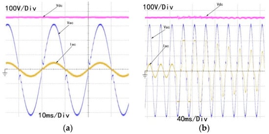
Figure 18.
(a) Output voltage, output current, and output voltage of the DC/AC converter. (b) Waveform with motor load.
In order to verify the performance of the inverter with a motor load, a 900 W AC motor load was suddenly applied to the resistance load. The resulting waveform is shown in Figure 18b. During the load change, the output power is 1800 W with a conversion efficiency of 96.7%, and the output is asymptotically stable.
5. Conclusions
This paper presents a PCMM power converter with three different working modes for EV application. The proposed PCMM can work in Bi-DC/DC, AC/DC, and DC/AC modes. In super-capacitor & battery hybrid energy storage systems for EV applications, the Bi-DC/DC mode converts the power between the battery and the super-capacitor; the AC/DC mode charges the battery, and the DC/AC mode provides an AC source to electrical equipment.
Mathematical representation of the state-space averaging model of the PCMM considering the resistance of IGBT and inductor is presented. Based on this model, the relationship between the steady state of the output voltage and the input voltage is given. In order to describe the system characteristics under small signal perturbations, the small signal model of the PCMM and the transfer function of the system are derived. Using the established PCMM model, the controller was designed. The simulation and experimental results show that the PCMM can meet the design target and the feasibility of the model is verified.
The PCMM converter reduces costs and lightens the system weight by sharing inductors, IGBT, capacitors, and other components. The measured results show that, compared with a traditional vehicle power conversion system, the PCMM structure proposed in this paper reduces the weight by 51.2%. The model presented in this paper reflects the characteristics of the system under small signal disturbances. In future research, the response characteristics of the system under state switching will be studied based on nonlinear modeling.
Author Contributions
Luo Yutao conceived the study. Wang Feng planned the experiments. Luo Yutao and Wang Feng wrote the manuscript. All authors submitted comments, read and approved the final manuscript.
Funding
This research was funded by the Major Research and Development Project of Guangdong Science and Technology Department, grant number 2016B010132001.
Conflicts of Interest
The authors declare no conflicts of interest.
Nomenclature
| EV | Electric vehicle |
| PFC | Power factor correction |
| Low side voltage (V) | |
| High side voltage (V) | |
| Switch of DC/AC | |
| Switch of AC/DC | |
| Switch of DC/DC | |
| , | IGBT of the first phase |
| , | IGBT of the second phase |
| , | Inductor (H) |
| Capacitor of the low side (F) | |
| Capacitor of the high side (F) | |
| Capacitor of the AC side (F) | |
| Voltage of the capacitor (V) | |
| Output voltage (V) | |
| Current small signal of (A) | |
| Current small signal of (A) | |
| Small signal of capacitor (V) | |
| PCMM | Power converter with multi-operating mode |
| THD | Total harmonic distortion |
| Voltage of AC side (V) | |
| Current of inductor (A) | |
| Current of inductor (A) | |
| The load resistance (Ω) | |
| Average output voltage in steady state (V) | |
| Average input voltage in steady state (V) | |
| Average capacitor voltage in steady state (V) | |
| , | Average current of inductor in steady state (A) |
| Inductor resistance (Ω) | |
| IGBT resistance (Ω) | |
| Input voltage (V) | |
| Duty cycle | |
| The reference voltage (V) | |
| Average voltage of capacitor in one cycle (V) | |
| Average current of in one cycle (A) | |
| Average current of in one cycle (A) |
References
- Ou, T.C.; Hong, C.M. Dynamic operation and control of microgrid hybrid power systems. Energy 2014, 66, 314–323. [Google Scholar] [CrossRef]
- Khaligh, A.; Li, Z.H. Battery, Ultracapacitor, Fuel Cell, and Hybrid Energy Storage Systems for Electric, Hybrid Electric, Fuel Cell, and Plug-In Hybrid Electric Vehicles: State of the Art. IEEE Trans. Veh. Technol. 2010, 59, 2806–2814. [Google Scholar] [CrossRef]
- Pahlevaninezhad, M.; Drobnik, J.; Jain, P.K.; Bakhshai, A. A Load Adaptive Control Approach for a Zero-Voltage-Switching DC/DC Converter Used for Electric Vehicles. IEEE Trans. Ind. Electron. 2012, 59, 920–933. [Google Scholar] [CrossRef]
- Pahlevaninezhad, M.; Das, P.; Drobnik, J.; Jain, P.K.; Bakhshai, A. A ZVS Interleaved Boost AC/DC Converter Used in Plug-in Electric Vehicles. IEEE Trans. Power Electron. 2012, 27, 3513–3529. [Google Scholar] [CrossRef]
- Sreeraj, E.S.; Chatterjee, K.; Bandyopadhyay, S. One-Cycle-Controlled Single-Stage Single-Phase Voltage-Sensorless Grid-Connected PV System. IEEE Trans. Ind. Electron. 2013, 60, 1216–1224. [Google Scholar]
- Ostadi, A.; Kazerani, M. A Comparative Analysis of Optimal Sizing of Battery-Only, Ultracapacitor-Only, and Battery-Ultracapacitor Hybrid Energy Storage Systems for a City Bus. IEEE Trans. Veh. Technol. 2015, 64, 4449–4460. [Google Scholar] [CrossRef]
- Ou, T.C.; Sciubba, E. Design of a Novel Voltage Controller for Conversion of Carbon Dioxide into Clean Fuels Using the Integration of a Vanadium Redox Battery with Solar Energy. Energies 2018, 11, 524. [Google Scholar] [CrossRef]
- Graditi, G.; Adinolfi, G.; Tina, G.M. Photovoltaic optimizer boost converters: Temperature influence and electro-thermal design. Appl. Energy 2014, 115, 140–150. [Google Scholar] [CrossRef]
- Wen, H.; Su, B. Hybrid-mode interleaved boost converter design for fuel cell electric vehicles. Energy Convers. Manag. 2016, 122, 477–487. [Google Scholar] [CrossRef]
- Pavlovsky, M.; Guidi, G.; Kawamura, A. Assessment of Coupled and Independent Phase Designs of Interleaved Multiphase Buck/Boost DC-DC Converter for EV Power Train. IEEE Trans. Power Electron. 2014, 29, 2693–2704. [Google Scholar] [CrossRef]
- Shahin, A.; Hinaje, M.; Martin, J.-P.; Pierfederici, S.; Rael, S.; Davat, B. High Voltage Ratio DC–DC Converter for Fuel-Cell Applications. IEEE Trans. Ind. Electron. 2010, 57, 3944–3955. [Google Scholar] [CrossRef]
- Urciuoli, D.P.; Tipton, C.W. Development of a 90 kW bi-directional DC-DC converter for power dense applications. In Proceedings of the IEEE Twenty-First Annual Applied Power Electronics Conference and Exposition (APEC’06), Dallas, TX, USA, 19–23 March 2006; p. 4. [Google Scholar]
- Garcia, O.; Zumel, P.; de Castro, A.; Cobos, J.A. Automotive DC-DC bidirectional converter made with many interleaved buck stages. IEEE Trans. Power Electron. 2006, 21, 578–586. [Google Scholar] [CrossRef]
- Zhang, W.; Feng, G.; Liu, Y.F.; Wu, B. A digital power factor correction (PFC) control strategy optimized for DSP. IEEE Trans. Power Electron. 2004, 19, 1474–1485. [Google Scholar] [CrossRef]
- Cho, Y.; Lai, J.S. Digital Plug-In Repetitive Controller for Single-Phase Bridgeless PFC Converters. IEEE Trans. Power Electron. 2013, 28, 165–175. [Google Scholar]
- De Souza, A.F.; Barbi, I. High power factor rectifier with reduced conduction and commutation losses. In Proceedings of the 21st International Telecommunication Energy Conference (INTELEC’99), Copenhagen, Denmark, 9 June 1999; pp. 82–90. [Google Scholar]
- Su, B.; Zhang, J.; Lu, Z. Totem-Pole Boost Bridgeless PFC Rectifier with Simple Zero-Current Detection and Full-Range ZVS Operating at the Boundary of DCM/CCM. IEEE Trans. Power Electron. 2011, 26, 427–435. [Google Scholar] [CrossRef]
- Dasgupta, S.; Sahoo, S.K.; Panda, S.K. Single-Phase Inverter Control Techniques for Interfacing Renewable Energy Sources with Microgrid—Part I: Parallel-Connected Inverter Topology with Active and Reactive Power Flow Control along with Grid Current Shaping. IEEE Trans. Power Electron. 2011, 26, 717–731. [Google Scholar] [CrossRef]
- Chen, A.; Shao, D.; Chunshui, D.U.; Zhang, C. High-frequency DC link flyback single phase inverter for grid-connected photovoltaic system. In Proceedings of the 2010 2nd IEEE International Symposium on Power Electronics for Distributed Generation Systems (PEDG), Hefei, China, 16–18 June 2010; pp. 364–367. [Google Scholar]
- Lee, J.Y.; Song, H.S.; Yoo, I.P.; Jang, K.Y.; Shin, S.; Joo, J.H. System for Recharging Plug-In Hybrid Vehicle and Control Method for the Same. United States Patent Application 20120049803, 1 March 2012. [Google Scholar]
- Dusmez, S.; Chen, C.; Khaligh, A. A reduced-part single stage direct AC/DC On-board charger for automotive applications. In Proceedings of the IEEE 2013 Twenty-Eighth Annual Applied Power Electronics Conference and Exposition (APEC), Long Beach, CA, USA, 17–21 March 2013; pp. 1791–1797. [Google Scholar]
- Dusmez, S.; Khaligh, A. A Charge-Nonlinear-Carrier-Controlled Reduced-Part Single-Stage Integrated Power Electronics Interface for Automotive Applications. IEEE Trans. Veh. Technol. 2014, 63, 1091–1103. [Google Scholar] [CrossRef]
- Ou, T.-C.; Lin, W.-M.; Huang, C.-H. A multi-input power converter for hybrid renewable energy generation system. In Proceedings of the 1st IEEE-PES/IAS Conference on Sustainable Alternative Energy (SAE 2009), Valencia, Spain, 28–30 September 2009. [Google Scholar]
- Sun, J.; Mitchell, D.M.; Greuel, M.F.; Krein, P.T.; Bass, R.M. Averaged modeling of PWM converters operating in discontinuous conduction mode. IEEE Trans. Power Electron. 2001, 16, 482–492. [Google Scholar]
- Maniktala, S. Switching Power Supplies A to Z; Newnes: Newton, MA, USA, 2012. [Google Scholar]
© 2018 by the authors. Licensee MDPI, Basel, Switzerland. This article is an open access article distributed under the terms and conditions of the Creative Commons Attribution (CC BY) license (http://creativecommons.org/licenses/by/4.0/).