1. Introduction
High switching frequency leads to power density enhancement in power converters [
1,
2,
3,
4,
5,
6,
7]. However, increasing switching frequencies sharply enlarges the power losses [
8,
9]. This increased power loss issue is particularly notable in low-voltage circuits, such as Point of Load (POL) circuits [
10]. For example, in [
11], gate drive losses account for 19% of the total power loss at a frequency of 100 kHz. Therefore, increasing switching frequency will significantly increase the power loss and reduce the power efficiency. As a consequence, reducing driving power loss is necessary in applications with high switching frequency.
Ref. [
12] proposed a resonant circuit in gate driver, and reduced the power loss from 122.02 mW to 64.5 mW [
13]. The principle involves injecting energy into the gate capacitance of a MOSFET drive using a resonant inductor. In contrast, conventional gate drivers (CGD) use a drive Resistance
to provide energy, with 50% of the energy lost in the drive resistance. This circuit effectively reduces driving losses.
However, resonant driving has not been widely applied in the industry [
14]. Compared to conventional driving schemes, resonant driving faces several issues:
Resonant gate drivers are susceptible to external interference [
13,
15,
16,
17,
18,
19]. When there is high-frequency external interference, the interference directly flows through the MOSFET’s gate capacitance rather than being bypassed by the driving circuit. This interference current causes voltage changes in the drive capacitor, potentially leading to system falsely turned ON/OFF. Conversely, in the conventional driver circuit, the
is clamped to ON/OFF voltages with
, and is relatively less susceptible to the external interference current.
Resonant gate drivers may encounter frequency mismatch between the resonant frequency and the control frequency [
15,
20,
21,
22,
23]. When the control frequency and the resonant frequency are not perfectly matched, the system may face issues such as overvoltage [
24], increased losses [
25], and over-resonance, severely affecting system reliability.
The losses in the resonant circuit are still high and need further reduction [
16,
26].
To solve the first issue, refs. [
27,
28,
29] proposes a resonant gate driver based on a half-bridge circuit structure, achieving
voltage clamping by enabling the upper and lower switches. However, significant energy loss occurs in the resonant circuit due to the body diode introduced in the MOSFETs, through which the current flows during operation [
30]. The structure presented in [
31] is similar to [
27], utilizing additional capacitors in the circuit to achieve negative voltage cutoff. However, the cutoff voltage is determined by the pre-charge current, leading to inappropriate cutoff voltage during fluctuations in circuit parameters. Ref. [
16] employs a full-bridge circuit structure, achieving voltage clamping by enabling the upper and lower switches in the right bridge arm. Nevertheless, the loss through the body diode during the energy recovery phase is non-negligible.
Ref. [
32] leverages the unidirectional conduction property of the MOSFET’s body diode to address the second issue. However, the body diode in the circuit also induces substantial conduction losses. Refs. [
33,
34,
35] adopt a similar approach by adding additional diodes to the resonant circuit to resolve the second issue. However, these diodes similarly result in significant conduction losses. The circuit proposed in [
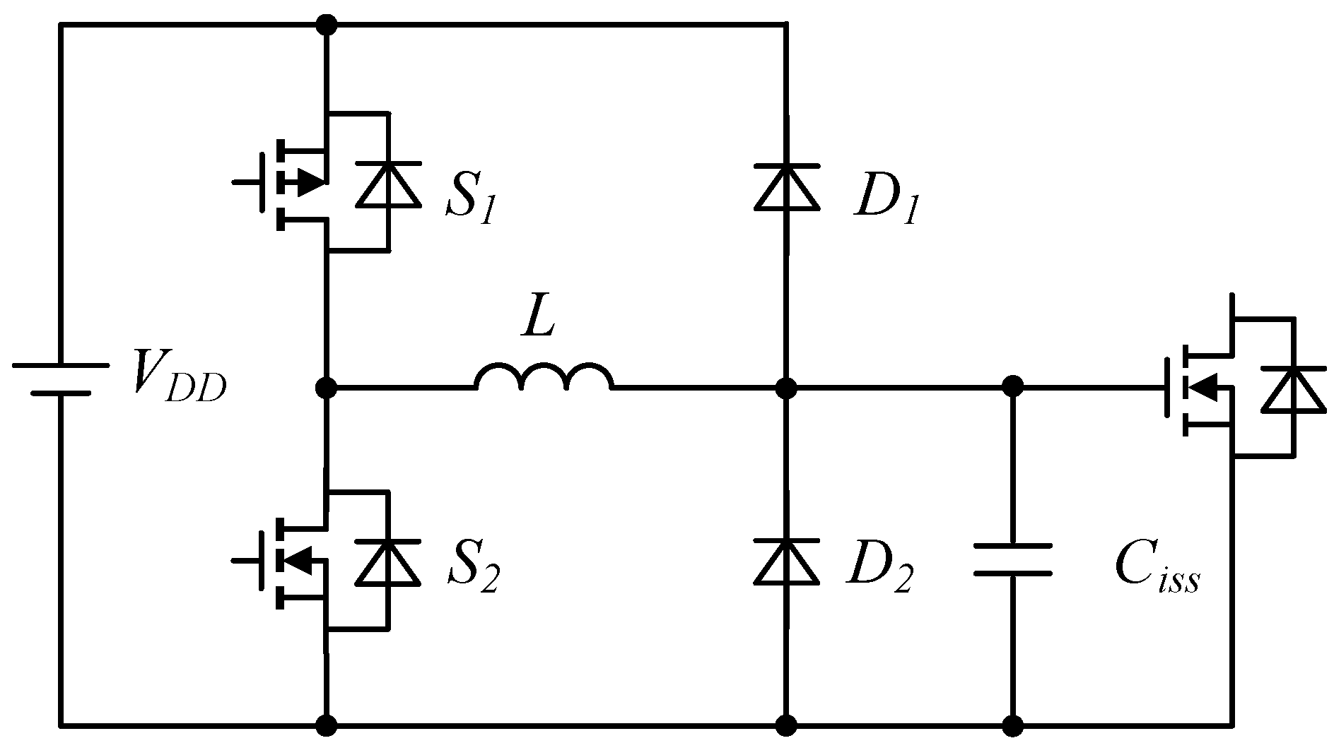
15], as shown in
Figure 1, exhibits high tolerance to pulse width variations, but the gate is clamped only during the energy recovery stage, and the diode in this stage introduces non-negligible losses.
The driver proposed in [
36,
37] achieves bidirectional voltage switching, with the energy transferred from the driven capacitor to the inductor returning to the capacitor with opposite voltage polarity, significantly reducing power losses. However, this method fails to address clamping and mismatch issues arising from parameter fluctuations. Refs. [
38,
39] adopts a full-bridge circuit structure, avoiding losses through the body diode with different operating timing and achieving voltage clamping. Nevertheless, mismatch issues arise due to parameter fluctuations.
This manuscript proposes a new resonant driving circuit topology, meeting all the three key requirements of reduced loss, reliable clamping, and stability in the face of frequency simultaneously. By utilizing the body diode of auxiliary MOSFETs, this design can operate stably even when the resonant frequency changes, achieving clamping through the conduction of the upper and lower tubes. In high-frequency resonant circuits, the conduction loss of diodes constitutes a significant percentage of the overall losses of driving losses. The circuit proposed in this paper avoids diode losses, further reducing driving losses.
The structure of this paper is as follows:
Section 2 introduces the circuit structure and working principle of the resonant driver;
Section 3 discusses the impact of errors on the sensitivity of the resonant gate driver;
Section 4 presents the parameter design process for the proposed gate driver;
Section 5 and
Section 6 cover simulation and experimental validation, respectively. Finally, the conclusions are drawn in
Section 7.
2. Circuit and Operation Principle
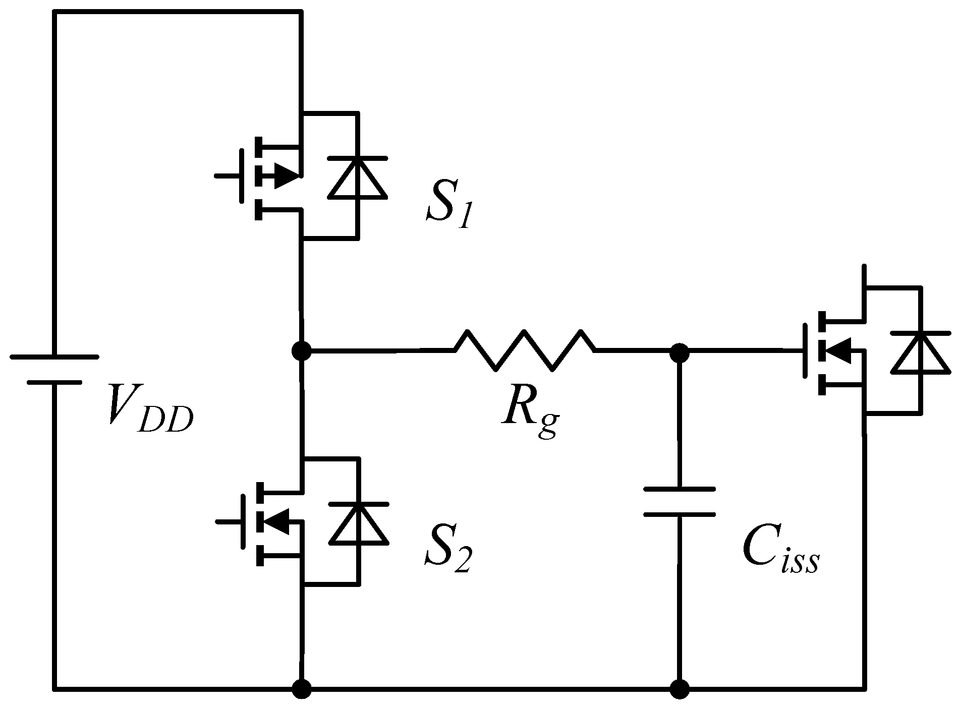
2.1. Gate Drivers Power Losses
Figure 2 illustrates the conventional gate driver circuit for the widely used power MOSFET, employing a totem pole topology. In conventional gate driver circuits, the losses are given by:
In addition to the losses, under high-frequency operating conditions, the losses associated with the auxiliary switch cannot be neglected. These include both the drive losses and switch losses.
Switch losses comprise switch capacitor losses and hard switch losses. Furthermore, the turn-on and turn-off of the traditional gate driver circuit can be equivalent to an RC circuit, where the switching time is constrained by the gate resistance and input capacitance. This results in slow drive speeds. Under high-frequency switching conditions, it becomes challenging to reduce gate losses effectively.
2.2. Existing Resonant Drivers
Resonant driving, achieved by incorporating a resonant inductor, serves to mitigate driving losses and, to a certain extent, expedite switching times. The majority of resonant driving topologies are based on half-bridge and full-bridge circuit structures. This approach aims to enhance the efficiency and performance of the driving circuit, contributing to a reduction in power losses and an improvement in switching dynamics.
Taking the structure in
Figure 1 as an example, the resonant circuit has four operational stages. In the first stage, switch
conducts, and LC resonance charges. The inductor current and
voltage start to rise until the current reaches its maximum value, and
voltage is
. In the second stage,
is turned off, and the inductor current continues to flow through the body diode of switch
, inductor, diode
, and
loop. The voltage across the input capacitor is clamped by diode
. In another operational stage, switch
conducts, and LC resonance discharges. Resonant drive losses include switch drive losses, conduction losses (equivalent resistance losses and diode losses), switch losses, and inductor losses.
In resonant drive circuits, beyond losses through resistive dissipation in the loop, it is imperative to consider losses incurred in the diodes within the circuit. The recovery path of energy following resonant charging and discharging traverses through the body diodes of MOSFETs and diodes. Consequently, within the losses of this resonant circuit, the impact of diode losses emerges as a significant factor that should not be disregarded. This recognition underscores the importance of comprehensively assessing and addressing diode-related losses for a more thorough understanding and optimization of resonant drive circuit performance.
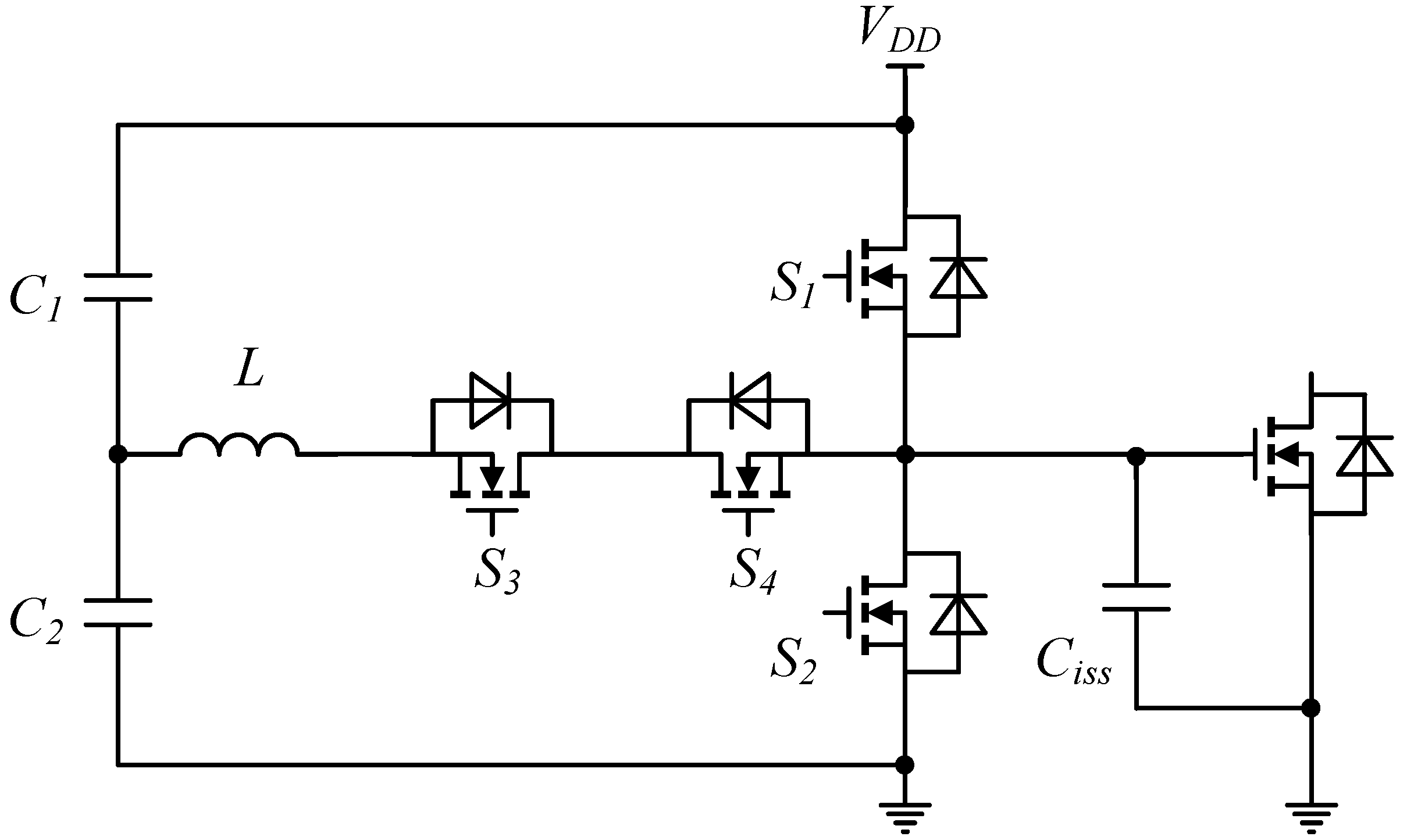
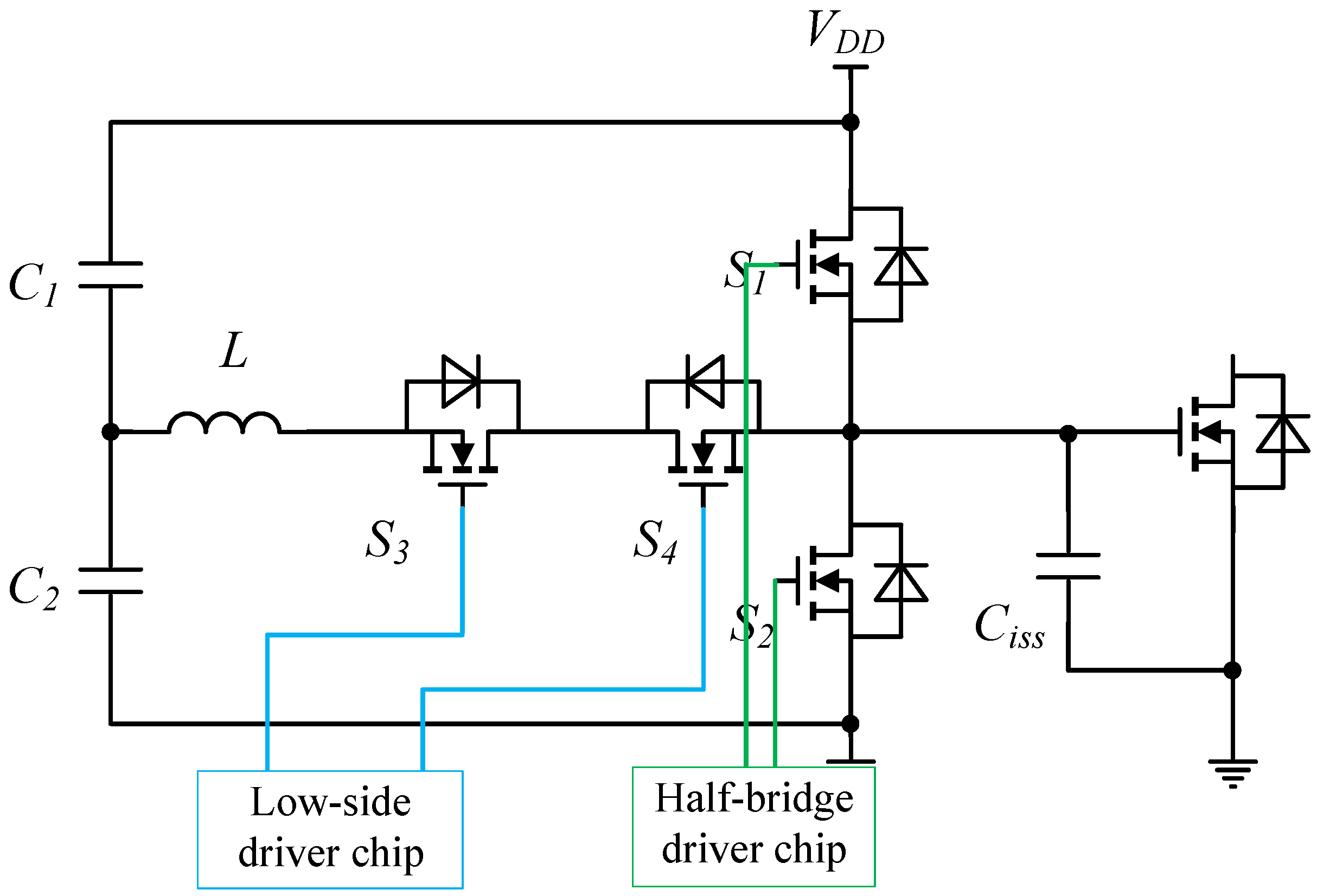
2.3. Proposed Resonant Circuit and Operation Principle
2.3.1. Operation Principle
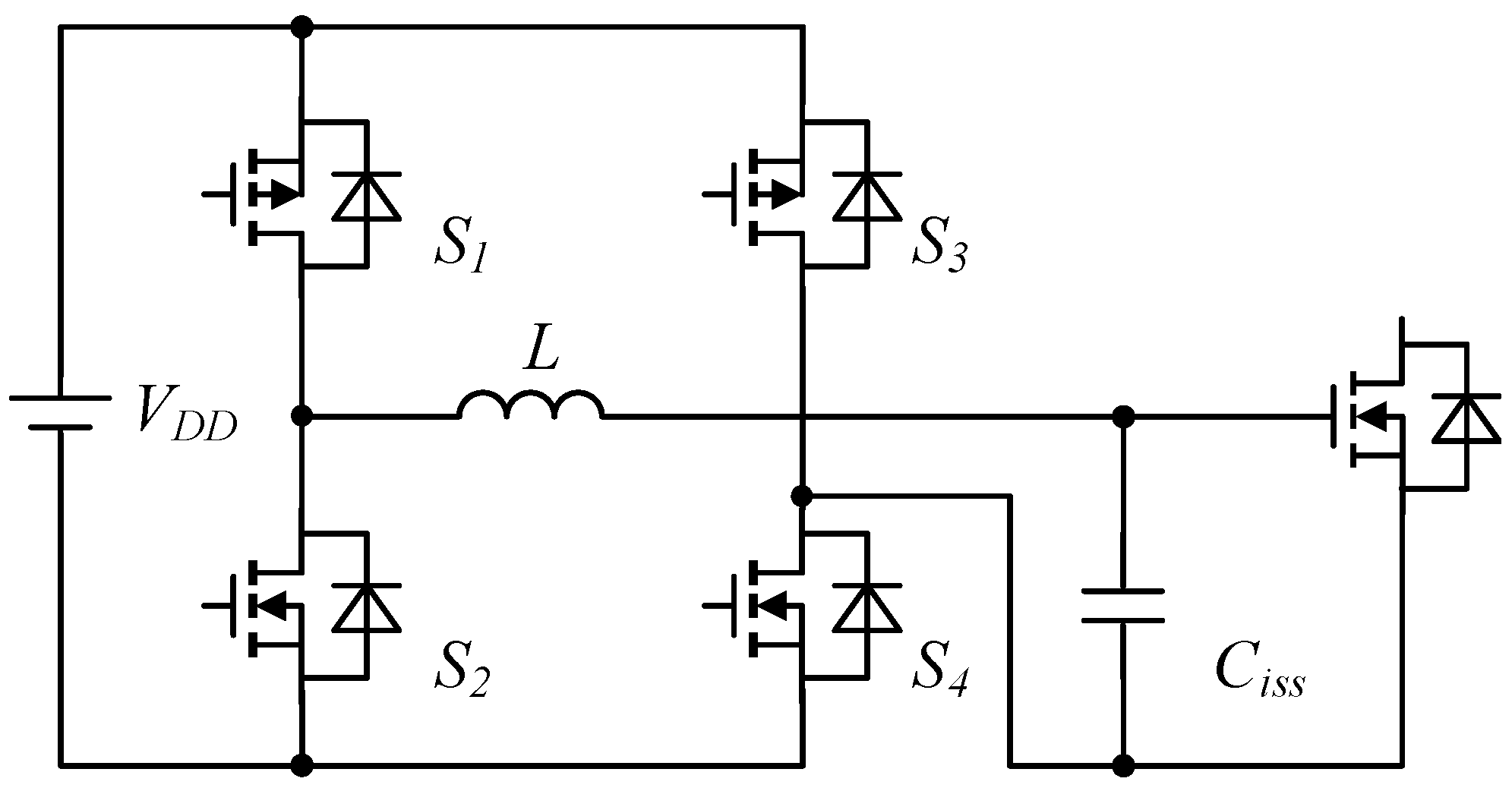
Recognizing the significance of diode losses in resonant gate drive circuits, this paper proposes a novel circuit topology aimed at further reducing the losses in the drive circuit. The proposed resonant drive circuit structure is illustrated in
Figure 3. This circuit comprises four N-channel MOSFETs, a resonant inductor (L), and capacitors (
and
). Capacitors
and
are utilized to evenly divide the supply voltage. By controlling the timing of four auxiliary switches, diode losses can be mitigated, thus achieving a more efficient resonant drive. The main waveforms of the resonant gate driver are depicted in
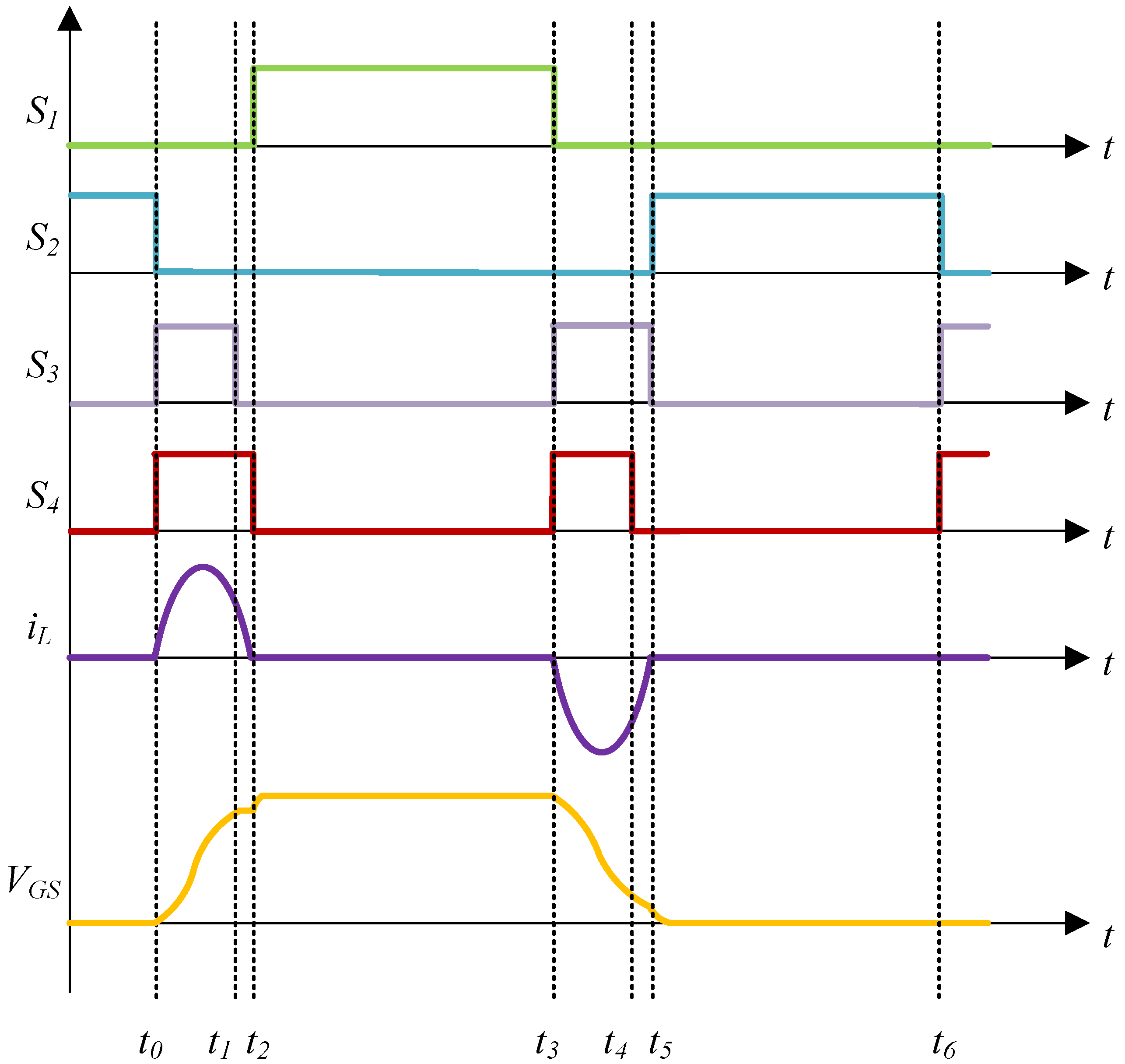
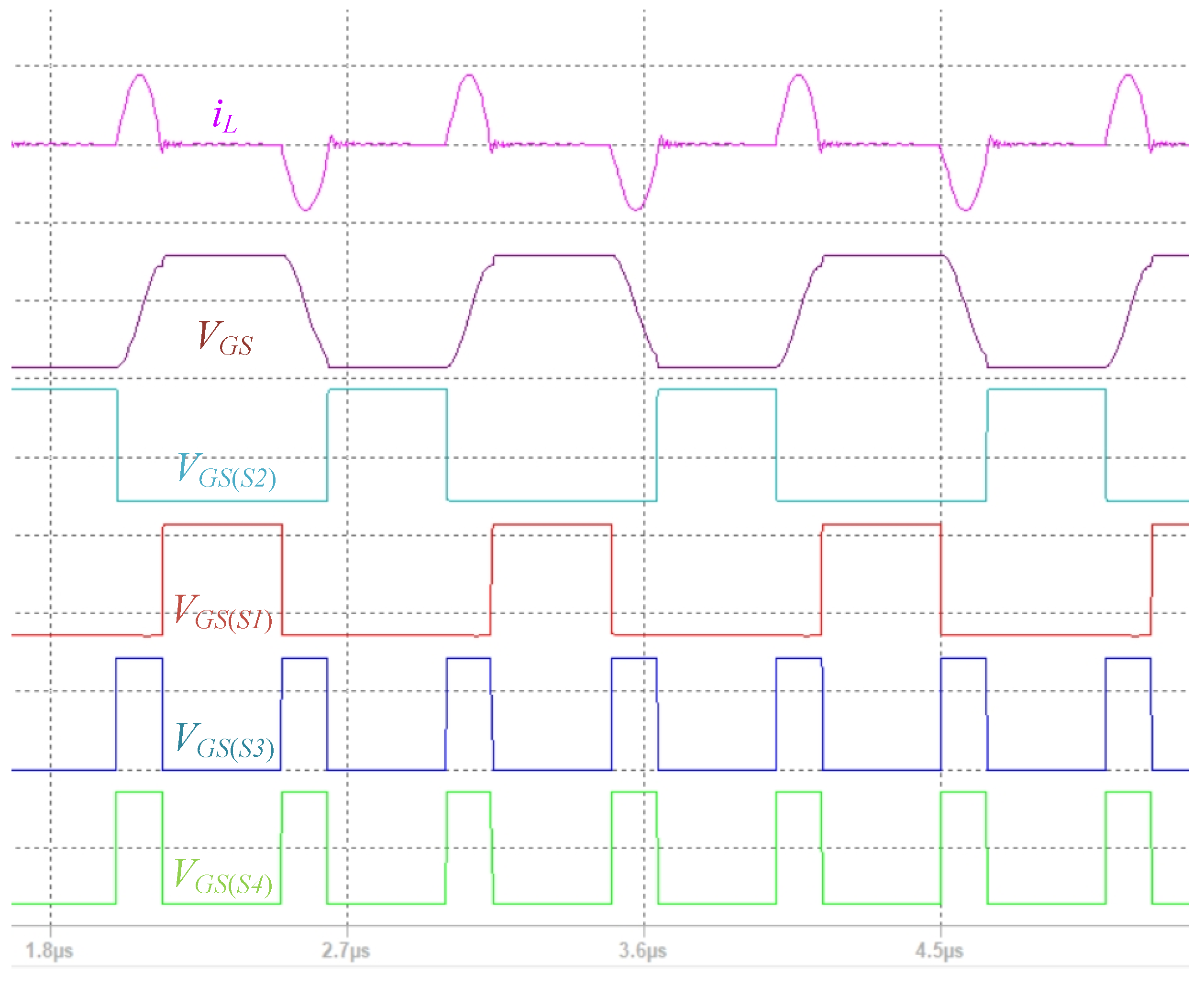
Figure 4.
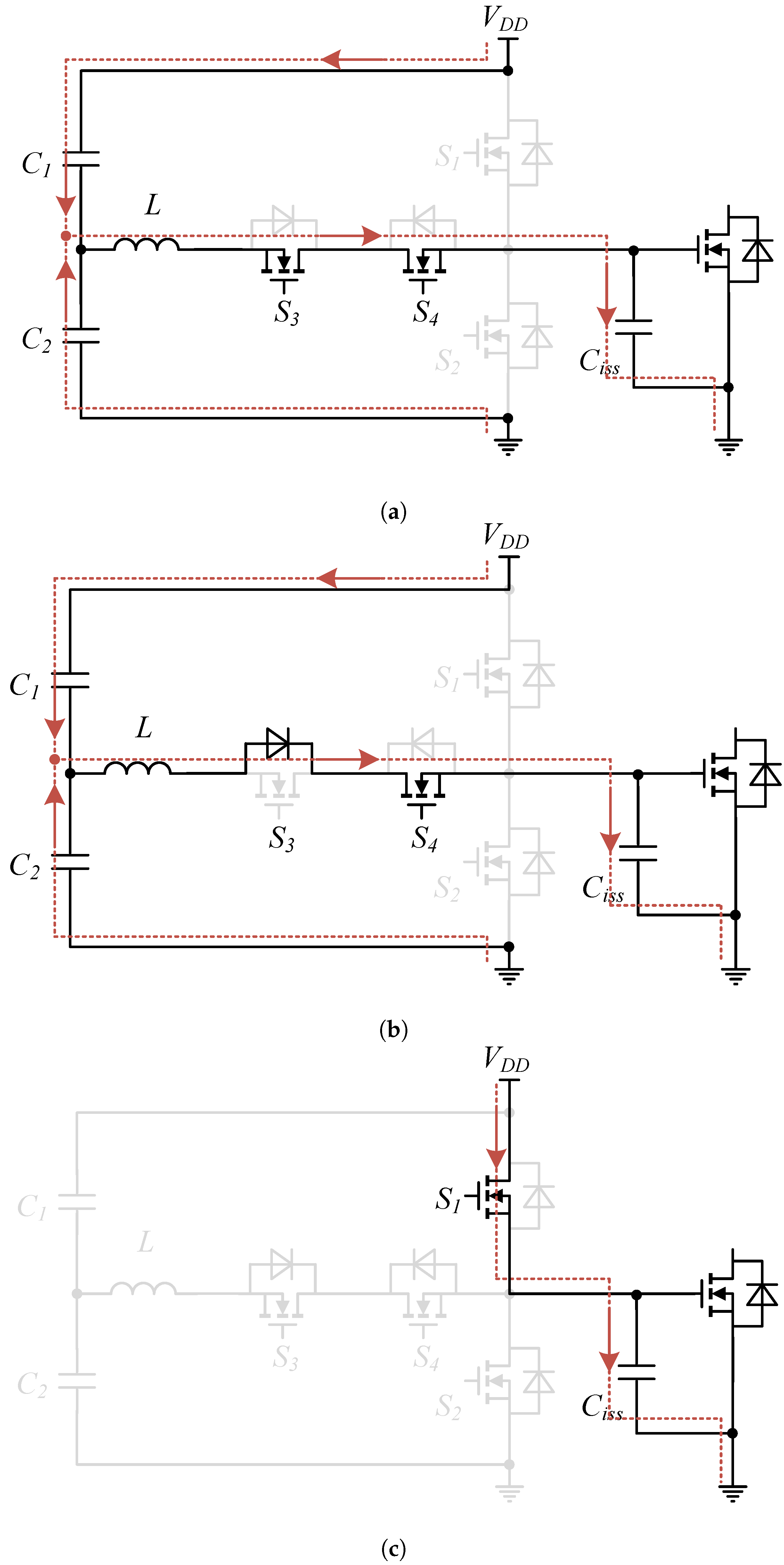
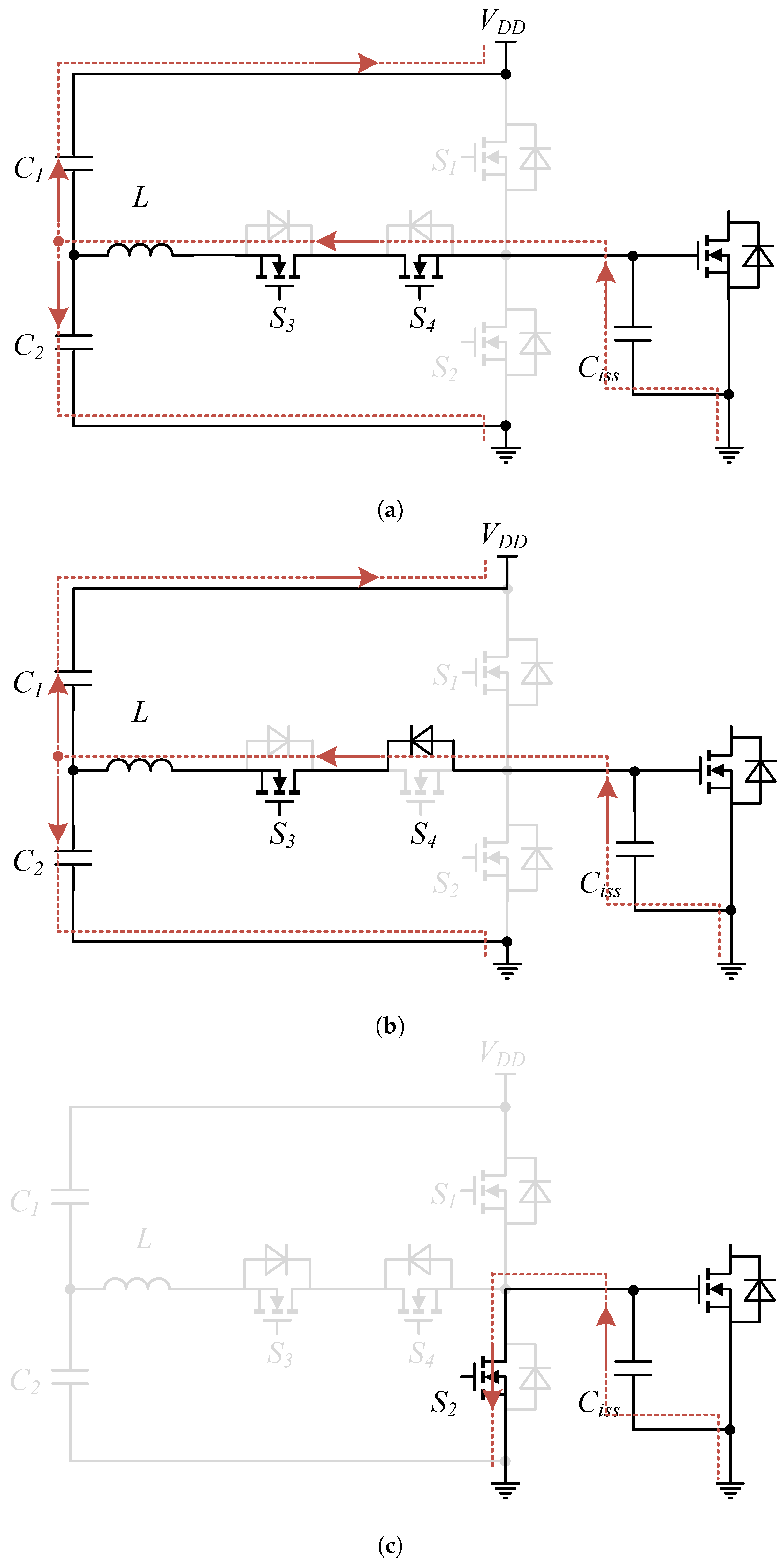
Figure 5 and
Figure 6 illustrate six operational modes of the resonant gate driver. These modes manifest sequentially in the order of time t0–t6. The intricacies of these modes are discussed below.
–: Before , only switch is conducting, and the gate-source voltage of the power MOSFET is clamped at zero volts through . At time , switches and conduct in a zero-current switching mode, treating capacitor as a voltage source for resonant charging of the inductor and power MOSFET gate capacitance. The current path is C-L---.
–: At , switch is turned off in advance, allowing the current to freewheel through the body diode of . When the current decreases to zero, the resonant charging stage ends due to the unidirectional conduction of the diode.
–: At , switches and are turned off, and switch is turned on. The gate-source voltage of the power MOSFET is connected to , and the gate-source voltage is clamped at . At , exactly halfway through the resonant period, the inductor current decreases to zero, and the gate-source voltage of the power MOSFET increases to , enabling switches and to turn off in a zero-current switching mode and switch to turn on in a zero-voltage switching mode.
–: At , switch turns off in a zero-voltage switching mode, and switches and conduct in a zero-current switching mode. starts to discharge, and its current path is ---L-C. The energy stored in is fed back to C.
–: At , switch is turned off in advance, allowing the current to freewheel through the body diode of . When the current decreases to zero, the resonant charging stage ends due to the unidirectional conduction of the diode.
–: At , the same principle applies. Switches and turn off in a zero-current switching mode, and switch turns on in a zero-voltage switching mode. The gate-source voltage is clamped at zero volts.
2.3.2. Loss Analysis
In the previous chapter, we discussed the turn-on and turn-off operations of switches under ZCS conditions and switches under ZVS conditions. Consequently, in the analysis of losses, the switch losses of the auxiliary switches were significantly reduced. Due to the relatively small and short-duration current flow through the body diode of the MOSFET, the associated losses are considered negligible in the loss calculation. The losses within the gate driver circuit encompass the driver losses of the MOSFETs, the conduction losses of the driver circuit, and the losses within the inductor.
The driver losses of the MOSFETs switch can be expressed as:
Here, represents the gate charge of the MOSFETs, and represents the gate-source voltage of the MOSFETs.
The resonant frequency can be calculated based on the selected inductance and the equivalent input capacitance. The resonant frequency can be expressed as
The resonance period can be expressed as
Resonance conduction loss can be expressed as
The angular frequency of damped resonance is denoted as
. Due to the relatively small value of
, the damped resonance angular frequency can be approximated as the undamped resonance angular frequency. The damping coefficient is
After a charging stage lasting half a resonant period, at this point, the voltage across
is
Subsequently, energy is replenished to
through the power supply, and clamping is applied. The current during this stage is
At this juncture, is equivalent to .
The energy replenishment stage involves
K is a constant. When K is greater than or equal to 3, the capacitor voltage approximately reaches its maximum value. It is recommended to set K as 3.
The inductive losses include copper loss and iron core loss. Copper loss is as follows:
The iron core loss is calculated using standard estimation methods. Compared to other losses, the iron core loss is relatively small and can be neglected. In addition, an air-core inductor is employed, and the iron loss is zero.
So, the total loss of the gate driver circuit can be expressed as:
3. Error to Sensitivity
The variation in the performance of inductor devices is a common phenomenon in power electronic circuits. One of the primary reasons influencing this variation is the temperature-induced impact on the magnetic core. With temperature fluctuations, the magnetic properties of the core undergo changes, leading to fluctuations in the crucial characteristics of the inductor.
Furthermore, hollow-core inductor devices are similarly susceptible to direct influences from the external environment. External factors such as humidity, temperature, and surrounding materials can significantly affect the performance of air-core inductors. Therefore, the ability of gate driver circuits to resist interference in situations of small-scale fluctuations in inductance values becomes crucial.
3.1. Existing Resonant Drive Circuit
The full-bridge resonant driving circuit is a common power electronic circuit, and its schematic diagram is shown in the
Figure 7. During the charging stage, when both lower MOSFETs are simultaneously turned on, resonance occurs between the resonant inductor and the input capacitance of the power MOSFET, causing the
voltage to change from
to
. Subsequently, the voltage across the input capacitance is maintained by turning on
. In the discharging stage, the same two lower MOSFETs are turned on, and resonance occurs between the inductor and capacitor, causing the input voltage to change to
. The voltage across the input capacitance is then maintained by turning on
.
In existing resonant driving circuits, if the inductance is influenced under certain conditions, causing its actual value to be smaller than the ideal value, the resonant period may be smaller than the ideal value, leading to the occurrence of over-resonance. The input voltage of the power MOSFET continues to resonate even after reaching its maximum value, causing the voltage to decrease from its peak. Therefore, during the voltage maintenance stage, the power source needs to provide additional charging to the input capacitance, resulting in increased energy losses.
On the other hand, when the inductance is larger than its actual value, the actual resonant period may be greater than the ideal resonant period. Assuming the charging phase has ended and both lower switches are turned off, if the resonance has not ended and the inductor current has not decreased to zero, the continuity of the inductor current through --L-- may lead to overvoltage.
Thus, fluctuations in the inductance value may cause instability in the output of the full-bridge resonant driving circuit, impacting the performance of the circuit.
3.2. The Proposed Resonant Drive Circuit
The proposed resonant driving circuit demonstrates outstanding stability in the face of minor fluctuations in the inductance value or other errors. Even with slight variations in the actual inductance value, the circuit maintains relatively stable performance, being less susceptible to excessive impacts. This error-tolerance capability makes the resonant driving circuit more reliable in practical engineering applications, especially when dealing with small-scale fluctuations in inductance values, compared to other driving circuits.
When the actual inductance value is small, the circuit successfully avoids over-resonance through cleverly designed driving timing sequences. In the resonant charging phase, by strategically timing the shutdown of switch , the current flows through the body diode of and , effectively concluding the resonant charging. As the inductor current decreases to zero, the resonant charging concludes through the unidirectional conduction of the diode. The same strategy applies in the discharge phase, where the timely shutdown of switch prevents over-resonance.
In the case of a larger actual inductance value, during the shutdown of switches and , the inductor current does not impact the voltage across the input capacitance. The inductor current continues to flow through the switches in the driving loop, ensuring the smooth operation of the circuit.
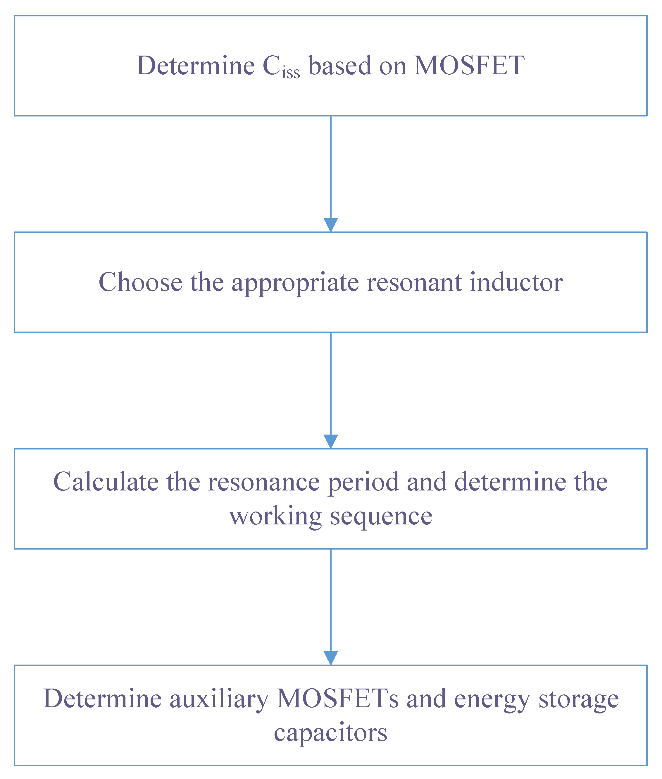
4. Parameter Design
The parameter design of the resonant circuit is shown in the
Figure 8.
- 1.
Determination of Power MOSFET Model:
Select a suitable Power MOSFET model, considering its input capacitance (), and calculate the total charge () to ensure that the drive circuit meets the design requirements.
- 2.
Selection of Resonant Inductor:
Consider the impact of the resonant inductor on the charging and discharging speed as well as the overall system efficiency. When selecting the inductor, strike a balance between the charging and discharging speed of the circuit and its efficiency, avoiding severe influence from the equivalent resistance () in the circuit. Choose an appropriate inductance value to enhance system efficiency while ensuring that the switch speed meets the requirements.
- 3.
Calculation of Resonant Period and Determination of Drive Timing:
Based on the selected values of capacitance and inductance, calculate the resonant period and subsequently determine the drive timing of the resonant circuit. Ensure that the timing design meets the stability and performance requirements of the circuit.
- 4.
Selection of Auxiliary Switch:
Choose an appropriate auxiliary switch to minimize conduction losses and drive losses. Ensure that the auxiliary switch operates stably in the circuit while meeting the design goals for performance and efficiency.
- 5.
Selection of Energy Storage Capacitor:
Consider the energy storage requirements of the system and select a suitable energy storage capacitor. Ensure that the chosen energy storage capacitor can meet the energy storage and release requirements of the circuit and maintain stability throughout the entire system.
Below is a numerical example for design and parameter selection.
The IRF3415S/LPbF is chosen as the power device to be driven. According to the datasheet, at
= 10 V,
is 200 nC, and consequently,
is determined to be 20 nF. Assuming the MOSFET’s switching speed should be less than 200 ns, based on (
4), the inductance value should be less than 202 nH. A larger inductance results in a higher quality factor of the resonant circuit, leading to lower energy loss. Considering energy loss and switching speed comprehensively, a 100 nH inductor is chosen for this example. According to (
4), the resonant period is 280 ns, and the drive timing of the switch is controlled through software. Without considering circuit resistance, estimating the peak current is below 4.47 A based on the formula
The IRLML6346 can meet the current-voltage requirements of the circuit. When the energy storage capacitor meets the voltage design requirements, the voltage drop should be minimized. In this case, a capacitor with a value three orders of magnitude higher than the input capacitor is chosen as the energy storage capacitor.
5. Simulation
Using Ltspice software (version 17.1.8 x64), the proposed resonant circuit was simulated to validate the rationality and feasibility of the circuit. The selection of the auxiliary switch model and parameters for the devices is presented in the table below. is added to the left side of the resonant inductor. The current waveform through the inductor can be obtained by measuring the voltage waveform across the sampling resistor.
According to the parameters of
and L in
Table 1, it can be calculated using (
4) that the resonant period is approximately 280 ns. Under stable system conditions at an operating frequency of 1 MHz, it is observed that the switching frequency of the
switch is 2 MHz, with an on-time of 140 ns, while the switching frequency of the
switch is 1 MHz, with an on-time of 360 ns.
Figure 9 illustrates the drive voltages and operational timing of each switch, along with the waveforms of inductor current and
voltage obtained under these operating conditions.
The original simulation files are attached in the multimedia folder.
Figure 10 presents the
under variations in inductance values, indicating that the resonant circuit can operate normally with a fluctuation of ±10% in inductance, ensuring system stability.
6. Experiment
Figure 11 illustrates the PCB board of the resonant drive circuit, with a length of 4.15 cm and a width of 2.87 cm. To facilitate testing, the PCB board is initially designed with larger dimensions, but optimization can be applied to make the PCB more compact. The PCB includes a 100 m
sampling resistor for capturing the current of the resonant inductor, and a 20 nF capacitor serves as the input capacitance for the equivalent power MOSFET. There are a total of six input ports, including four input drive signals,
, and GND.
Drive four auxiliary switches through a half-bridge driver chip and a low-side driver chip. The driver chip is a meticulously designed integrated circuit that controls the gate of a MOSFET by delivering essential signals, thereby regulating the MOSFET’s switching between the on and off states.
Figure 12 shows the circuit diagram after adding a low-side driver chip that drives switches
and a half-bridge driver chip that drives half-bridge switches
.
Table 2 provides the model numbers of the driver chips used in the experiment.
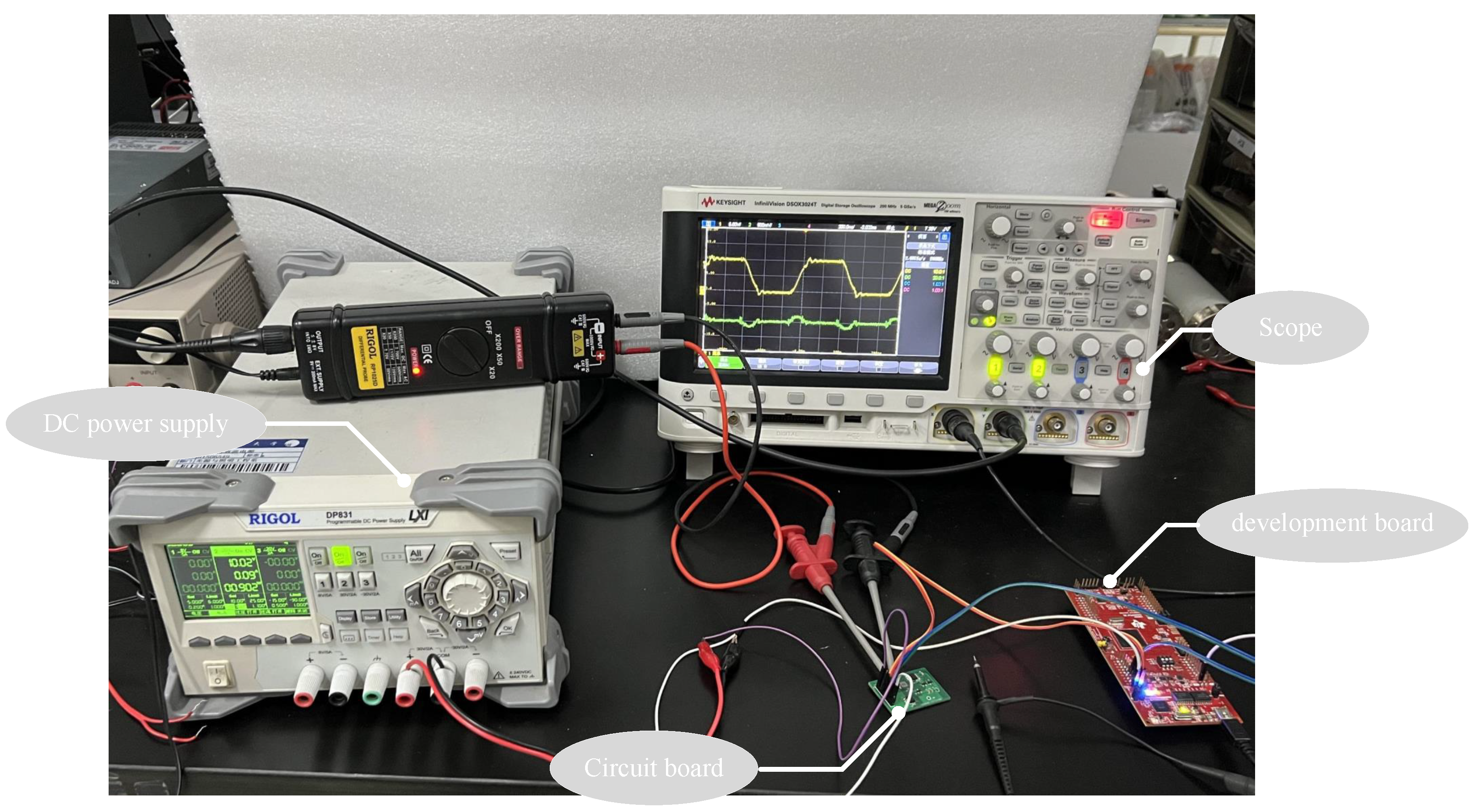
Figure 13 illustrates the experimental platform employed for the resonant gate driver. The utilized development board, namely LAUNCHXL-F28379D, has been programmed to generate customized fundamental drive signals tailored for the specific characteristics of the investigated circuit. The power supply equipment utilized in the experimental setup is the RIGOL DP831, capable of delivering a direct current (DC) voltage of 10 V.
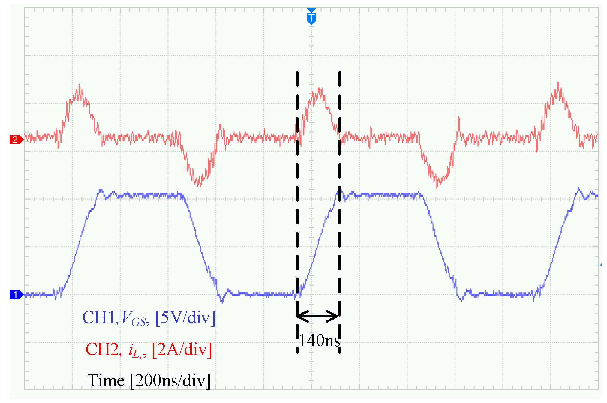
Figure 14 depicts the waveforms of
and
. The experimental setup operates at a switching frequency of 1 MHz, with a peak current of 2 A in the inductor during resonance. After resonant charging stage, the voltage of the output
remains stably at 10 V.
The table below illustrates the power losses of the CGD circuit, utilizing the circuit structure depicted in
Figure 2, and the proposed resonant gate drive circuit. The comparison is made between power with the Driver Chip Loss and power without the Driver Chip Loss, showcasing the percentage reduction in power consumption for the proposed circuit compared to the conventional gate drive circuit.
As indicated in
Table 3, for the proposed resonant gate drive circuit with the inclusion of the drive chip, the power loss is reduced by 63.68% compared to the CGD. And in the absence of the drive chip, the power loss reduction reaches 83.30% compared to the CGD. This shows the significant improvement in power efficiency achieved by the proposed resonant gate drive circuit.
The experimental results indicate that the proposed resonant gate drive circuit exhibits higher efficiency and a smaller footprint compared to existing drive circuits.
It is noteworthy that when the actual value of the inductance is biased towards a higher value in resonant driving, the inductor current at the end of resonance does not decrease to zero. Consequently, the inductor current cannot continue flowing through the original circuit. At this point, switch
experiences overvoltage across its terminals.
Figure 15 illustrates the situation of the drain-source voltage across
switch under normal conditions and during hard turn-off. Within a small error range of inductance values, the generated overvoltage remains within the rated
range of the MOSFET. Despite the circuit exhibiting robust anti-interference capabilities and stability in practical design, the potential impact on the switch should not be overlooked.
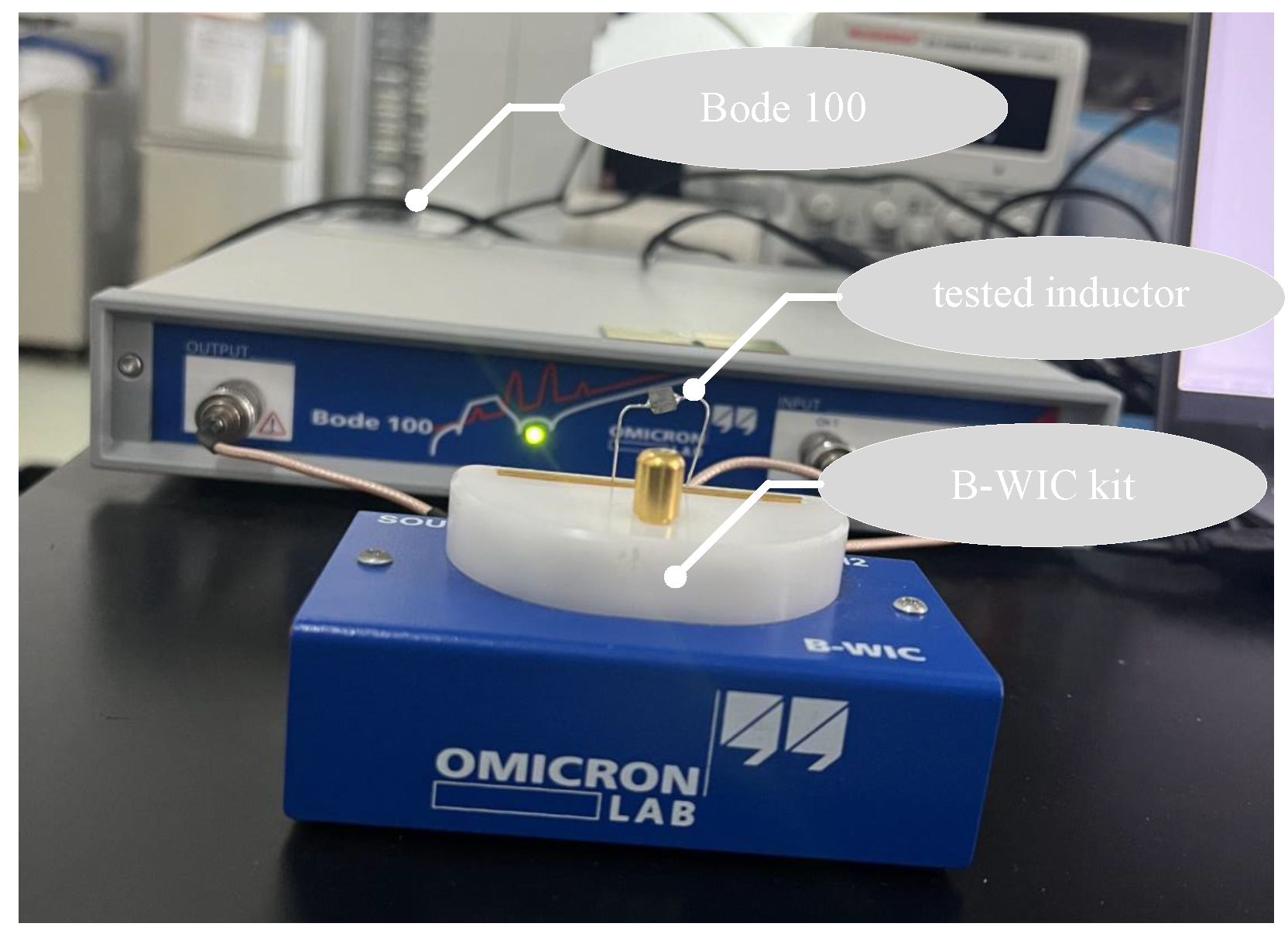
The inductance of 131 nH was achieved by adjusting the winding configuration on the existing 100 nH inductor.
Figure 16 illustrates the impedance testing of the inductor using the Bode 100.
Figure 17 depicts the test results, showing an inductance value of 131 nH at a working frequency of 1 MHz.
7. Conclusions
This paper proposes a resonant gate driving circuit with active clamping. Similar to the existing resonant gate drivers, the proposed circuit employs ZCS and ZVS to mitigate switching losses. In addition to the resonant driving effect, the proposed circuit has the following contributions:
The circuit is able to stabilize by the proposed active-clamp bridge, effectively preventing fluctuations.
The simultaneous switching of and avoids diode losses, thereby enhancing the overall system efficiency.
The control of switch scheme can mitigate the adverse effect cause by the mismatch between the resonant frequency and the control frequency.
Experimental validation shows that at = 1 MHz, the power consumption was reduced by 63.68%. Excluding the power consumption of the half-bridge and the low-side driver chips, the overall power reduction reached 83.30%.
Author Contributions
Conceptualization, H.Z.; methodology, J.Z. and H.Z.; software, J.Z. and Y.D.; validation, W.Y. and D.C.; formal analysis, J.Z.; investigation, W.Y. and D.C.; resources, Y.D. and W.Y.; data curation, J.Z. and W.Y.; writing—original draft preparation, J.Z.; writing—review and editing, J.Z.; visualization, J.Z.; supervision, J.Q.; project administration, K.L.; funding acquisition, H.Z. All authors have read and agreed to the published version of the manuscript.
Funding
This research was funded by New PI: na.
Data Availability Statement
Conflicts of Interest
The authors declare no conflict of interest.
References
- Thummala, P.; Yelaverthi, D.B.; Zane, R.A.; Ouyang, Z.; Andersen, M.A. A 10-MHz GaNFET-based-isolated high step-down DC–DC converter: Design and magnetics investigation. IEEE Trans. Ind. Appl. 2019, 55, 3889–3900. [Google Scholar] [CrossRef]
- Kruse, K.; Elbo, M.; Zhang, Z. GaN-based high efficiency bidirectional DC-DC converter with 10 MHz switching frequency. In Proceedings of the 2017 IEEE Applied Power Electronics Conference and Exposition (APEC), Tampa, FL, USA, 26–30 March 2017; pp. 273–278. [Google Scholar]
- Forouzesh, M.; Siwakoti, Y.P.; Gorji, S.A.; Blaabjerg, F.; Lehman, B. Step-up DC–DC converters: A comprehensive review of voltage-boosting techniques, topologies, and applications. IEEE Trans. Power Electron. 2017, 32, 9143–9178. [Google Scholar] [CrossRef]
- Zhao, S.; Blaabjerg, F.; Wang, H. An overview of artificial intelligence applications for power electronics. IEEE Trans. Power Electron. 2020, 36, 4633–4658. [Google Scholar] [CrossRef]
- Fassi, Y.; Heiries, V.; Boutet, J.; Boisseau, S. Towards Physics-Informed Machine Learning-Based Predictive Maintenance for Power Converters—A Review. IEEE Trans. Power Electron. 2023, 39, 2692–2720. [Google Scholar] [CrossRef]
- Hasanpour, S.; Lee, S.S. New Step-Up DC/DC Converter with Ripple Free Input Current. IEEE Trans. Power Electron. 2023, 7, 3023–3032. [Google Scholar] [CrossRef]
- Fani, R.; Akhlaghi, Z.; Adib, E. High Step-Up DC-DC Converter by Integration of Active Switched Inductors, Built In Transformer, and Multipliers. IEEE Trans. Power Electron. 2023, 39, 2468–2477. [Google Scholar] [CrossRef]
- Hou, R.; Shen, Y.; Zhao, H.; Hu, H.; Lu, J.; Long, T. Power loss characterization and modeling for GaN-based hard-switching half-bridges considering dynamic on-state resistance. IEEE Trans. Transp. Electrif. 2020, 6, 540–553. [Google Scholar] [CrossRef]
- Zhao, H.; Shen, Y.; Ying, W.; Ghosh, S.S.; Ahmed, M.R.; Long, T. A single-and three-phase grid compatible converter for electric vehicle on-board chargers. IEEE Trans. Power Electron. 2019, 35, 7545–7562. [Google Scholar] [CrossRef]
- Zhao, H.; Shen, Y.; Ying, W.; Qi, J.; Jiang, C.; Long, T. Mixed Analog–Digital (MAD) Converters for High Power Density DC–DC Conversions. IEEE Trans. Power Electron. 2020, 35, 7742–7748. [Google Scholar] [CrossRef]
- Ye, Z.; Lei, Y.; Pilawa-Podgurski, R.C. The cascaded resonant converter: A hybrid switched-capacitor topology with high power density and efficiency. IEEE Trans. Power Electron. 2019, 35, 4946–4958. [Google Scholar] [CrossRef]
- De Vries, I.D. A resonant power MOSFET/IGBT gate driver. In Proceedings of the APEC—Seventeenth Annual IEEE Applied Power Electronics Conference and Exposition (Cat. No. 02CH37335), Dallas, TX, USA, 10–14 March 2002; Volume 1, pp. 179–185. [Google Scholar]
- Chennu, J.V.P.S.; Maheshwari, R. Study on Resonant Gate Driver circuits for high frequency applications. In Proceedings of the 2016 IEEE 6th International Conference on Power Systems (ICPS), New Delhi, India, 4–6 March 2016; pp. 1–6. [Google Scholar]
- Yi, F.; Wang, F. Review of Voltage-Bucking/Boosting Techniques, Topologies, and Applications. Energies 2023, 16, 842. [Google Scholar] [CrossRef]
- Chen, Y.; Lee, F.C.; Amoroso, L.; Wu, H.P. A resonant MOSFET gate driver with efficient energy recovery. IEEE Trans. Power Electron. 2004, 19, 470–477. [Google Scholar] [CrossRef]
- Eberle, W.; Zhang, Z.; Liu, Y.F.; Sen, P.C. A current source gate driver achieving switching loss savings and gate energy recovery at 1-MHz. IEEE Trans. Power Electron. 2008, 23, 678–691. [Google Scholar] [CrossRef]
- Nguyen, V.S.; Lefranc, P.; Crebier, J.C. Gate driver supply architectures for common mode conducted EMI reduction in series connection of multiple power devices. IEEE Trans. Power Electron. 2018, 33, 10265–10276. [Google Scholar] [CrossRef]
- Balcells, J.; Bogonez-Franco, P. Effect of driver to gate coupling circuits on EMI produced by SiC MOSFETS. In Proceedings of the 2013 International Symposium on Electromagnetic Compatibility, Denver, CO, USA, 5–9 August 2013; pp. 209–214. [Google Scholar]
- Dymond, H.C.; Wang, J.; Liu, D.; Dalton, J.J.; McNeill, N.; Pamunuwa, D.; Hollis, S.J.; Stark, B.H. A 6.7-GHz active gate driver for GaN FETs to combat overshoot, ringing, and EMI. IEEE Trans. Power Electron. 2017, 33, 581–594. [Google Scholar] [CrossRef]
- Bešić, H.; Demir, A.; Steurer, J.; Luhmann, N.; Schmid, S. Schemes for Tracking Resonance Frequency for Micro-and Nanomechanical Resonators. Phys. Rev. Appl. 2023, 20, 024023. [Google Scholar] [CrossRef]
- Wang, Y.; Lucia, O.; Zhang, Z.; Gao, S.; Guan, Y.; Xu, D. A review of high frequency power converters and related technologies. IEEE Open J. Ind. Electron. Soc. 2020, 1, 247–260. [Google Scholar] [CrossRef]
- Mahesh, M.; Kumar, K.V.; Abebe, M.; Udayakumar, L.; Mathankumar, M. A review on enabling technologies for high power density power electronic applications. Mater. Today Proc. 2021, 46, 3888–3892. [Google Scholar] [CrossRef]
- Jafari, A.; Nikoo, M.S.; Perera, N.; Yildirim, H.K.; Karakaya, F.; Soleimanzadeh, R.; Matioli, E. Comparison of wide-band-gap technologies for soft-switching losses at high frequencies. IEEE Trans. Power Electron. 2020, 35, 12595–12600. [Google Scholar] [CrossRef]
- Xu, J.; Yang, X.; Zhao, H.; Qiu, J.; Liu, K. An Inductor-Based and Capacitor-Free Bipolar Pulse Converter with Overvoltage Protection. World Electr. Veh. J. 2022, 13, 91. [Google Scholar] [CrossRef]
- Yang, X.; Zhao, Z.; Wang, C.; Xu, J.; Liu, K.; Qiu, J. Analysis and Parameter Design of SiC-Based Current Source Inverter (CSI). World Electr. Veh. J. 2022, 13, 187. [Google Scholar] [CrossRef]
- Henn, J.; Lüdecke, C.; Laumen, M.; Beushausen, S.; Kalker, S.; van der Broeck, C.H.; Engelmann, G.; de Doncker, R.W. Intelligent gate drivers for future power converters. IEEE Trans. Power Electron. 2021, 37, 3484–3503. [Google Scholar] [CrossRef]
- Zhang, Z.; Fu, J.; Liu, Y.F.; Sen, P.C. Discontinuous-current-source drivers for high-frequency power MOSFETs. IEEE Trans. Power Electron. 2010, 25, 1863–1876. [Google Scholar] [CrossRef]
- Zhang, J.; Wu, H.; Zhao, J.; Zhang, Y.; Zhu, Y. A resonant gate driver for silicon carbide MOSFETs. IEEE Access 2018, 6, 78394–78401. [Google Scholar] [CrossRef]
- Pan, S.; Jain, P. A new pulse resonant MOSFET gate driver with efficient energy recovery. In Proceedings of the 2006 37th IEEE Power Electronics Specialists Conference, Jeju, Republic of Korea, 18–22 June 2006; pp. 1–5. [Google Scholar]
- Jovanovic, M.M.; Zhang, M.T.; Lee, F.C. Evaluation of synchronous-rectification efficiency improvement limits in forward converters. IEEE Trans. Ind. Electron. 1995, 42, 387–395. [Google Scholar] [CrossRef]
- Chen, R.; Peng, F.Z. A high-performance resonant gate-drive circuit for MOSFETs and IGBTs. IEEE Trans. Power Electron. 2013, 29, 4366–4373. [Google Scholar] [CrossRef]
- Fujita, H. A resonant gate-drive circuit with optically isolated control signal and power supply for fast-switching and high-voltage power semiconductor devices. IEEE Trans. Power Electron. 2013, 28, 5423–5430. [Google Scholar] [CrossRef]
- Chennu, J.V.P.S.; Maheshwari, R.; Li, H. New resonant gate driver circuit for high-frequency application of silicon carbide MOSFETs. IEEE Trans. Ind. Electron. 2017, 64, 8277–8287. [Google Scholar] [CrossRef]
- Rafiq, A.; Maheshwari, R. A resonant gate driver circuit with turn-on and turn-off dv/dt control. In Proceedings of the 2018 IEEMA Engineer Infinite Conference (eTechNxT), New Delhi, India, 13–14 March 2018; pp. 1–5. [Google Scholar]
- Swamy, M.M.; Kume, T.; Takada, N. An efficient resonant gate-drive scheme for high-frequency applications. IEEE Trans. Ind. Appl. 2012, 48, 1418–1431. [Google Scholar] [CrossRef]
- Fujita, H. A resonant gate-drive circuit capable of high-frequency and high-efficiency operation. IEEE Trans. Power Electron. 2009, 25, 962–969. [Google Scholar] [CrossRef]
- Li, F.F.; Zhang, Z.; Liu, Y.F. A novel dual-channel isolated resonant gate driver to achieve gate drive loss reduction for ZVS full-bridge converters. In Proceedings of the 7th International Power Electronics and Motion Control Conference, Harbin, China, 2–5 June 2012; Volume 2, pp. 936–940. [Google Scholar]
- Eberle, W.; Liu, Y.F.; Sen, P.C. A new resonant gate-drive circuit with efficient energy recovery and low conduction loss. IEEE Trans. Ind. Electron. 2008, 55, 2213–2221. [Google Scholar] [CrossRef]
- Long, Y.; Zhang, W.; Costinett, D.; Blalock, B.B.; Jenkins, L.L. A high-frequency resonant gate driver for enhancement-mode GaN power devices. In Proceedings of the 2015 IEEE Applied Power Electronics Conference and Exposition (APEC), Charlotte, NC, USA, 15–19 March 2015; pp. 1961–1965. [Google Scholar]
Figure 1.
Resonant gate driver with efficient energy recovery in [
15].
Figure 1.
Resonant gate driver with efficient energy recovery in [
15].
Figure 2.
Conventional gate drivers (CGD).
Figure 2.
Conventional gate drivers (CGD).
Figure 3.
Proposed resonant gate driver with active clamping.
Figure 3.
Proposed resonant gate driver with active clamping.
Figure 4.
Switching states of MOSFETs and waveforms of and .
Figure 4.
Switching states of MOSFETs and waveforms of and .
Figure 5.
Equivalent circuits of each stage during turn-on transition, (a) resonant charging stage, [], (b) reverse current mitigation stage, [], (c) clamping stage, [].
Figure 5.
Equivalent circuits of each stage during turn-on transition, (a) resonant charging stage, [], (b) reverse current mitigation stage, [], (c) clamping stage, [].
Figure 6.
Equivalent circuits of each stage during turn-off transition, (a) resonant discharging stage, [], (b) reverse current mitigation stage, [], (c) clamping stage, [].
Figure 6.
Equivalent circuits of each stage during turn-off transition, (a) resonant discharging stage, [], (b) reverse current mitigation stage, [], (c) clamping stage, [].
Figure 7.
Resonant gate driver capable of high-frequency and high- efficiency operation in [
36].
Figure 7.
Resonant gate driver capable of high-frequency and high- efficiency operation in [
36].
Figure 8.
Parameter design flow chart.
Figure 8.
Parameter design flow chart.
Figure 9.
The simulated switching state of MOSFETs and the waveforms of and .
Figure 9.
The simulated switching state of MOSFETs and the waveforms of and .
Figure 10.
Impact of inductor value variations on .
Figure 10.
Impact of inductor value variations on .
Figure 11.
The proposed resonant gate driver circuit board.
Figure 11.
The proposed resonant gate driver circuit board.
Figure 12.
Driver circuit connection diagram.
Figure 12.
Driver circuit connection diagram.
Figure 13.
Experimental setup.
Figure 13.
Experimental setup.
Figure 14.
and during switching transitions.
Figure 14.
and during switching transitions.
Figure 15.
Impact of inductor on of Switch , (a) L = 100 nH, (b) L = 131 nH.
Figure 15.
Impact of inductor on of Switch , (a) L = 100 nH, (b) L = 131 nH.
Figure 16.
Impedance test using a Bode 100 with a B-WIC kit.
Figure 16.
Impedance test using a Bode 100 with a B-WIC kit.
Figure 17.
Inductance measurement results: phase, impedance, and inductance.
Figure 17.
Inductance measurement results: phase, impedance, and inductance.
Table 1.
The parameters of the resonant gate driver.
Table 1.
The parameters of the resonant gate driver.
| Parameter | Value | Parameter | Value |
|---|
| 20 nF | | 10 V |
| IRLML6346 | L | 100 nH |
| C | 10
μF | | 100 m |
Table 2.
Driver chip selection table.
Table 2.
Driver chip selection table.
| Driver Chip Type | Model Name |
|---|
| Low Side | UCC27324DR |
| Half Bridge | LM5101A |
Table 3.
Power loss comparison of CGD and proposed resonant gate drive at 1 MHz.
Table 3.
Power loss comparison of CGD and proposed resonant gate drive at 1 MHz.
| Type | Power with Driver Chip Loss | Power without Driver Chip Loss |
|---|
|
Power Loss
|
Reduction
|
Power Loss
|
Reduction
|
|---|
| CGD circuit | 2512.89 mW | _ | 2185.72 mW | _ |
| Proposed circuit | 912.64 mW | 63.68% | 364.93 mW | 83.30% |
| Disclaimer/Publisher’s Note: The statements, opinions and data contained in all publications are solely those of the individual author(s) and contributor(s) and not of MDPI and/or the editor(s). MDPI and/or the editor(s) disclaim responsibility for any injury to people or property resulting from any ideas, methods, instructions or products referred to in the content. |
© 2024 by the authors. Licensee MDPI, Basel, Switzerland. This article is an open access article distributed under the terms and conditions of the Creative Commons Attribution (CC BY) license (https://creativecommons.org/licenses/by/4.0/).


 ,
, 


