Direct Power Control of a Bipolar Output Active Rectifier for More Electric Aircraft Based on an Optimized Sector Division
Abstract
1. Introduction
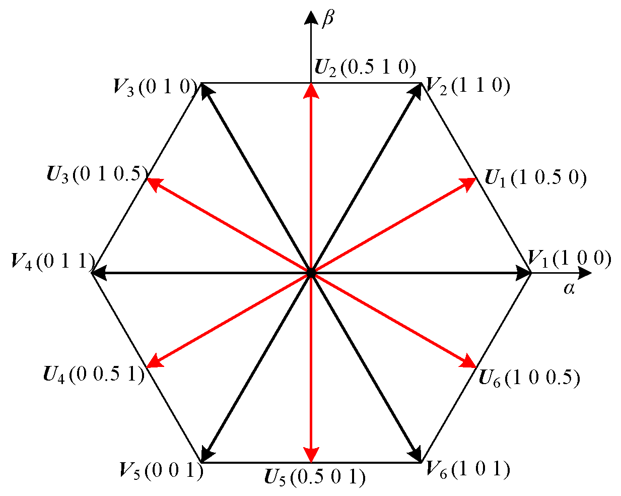
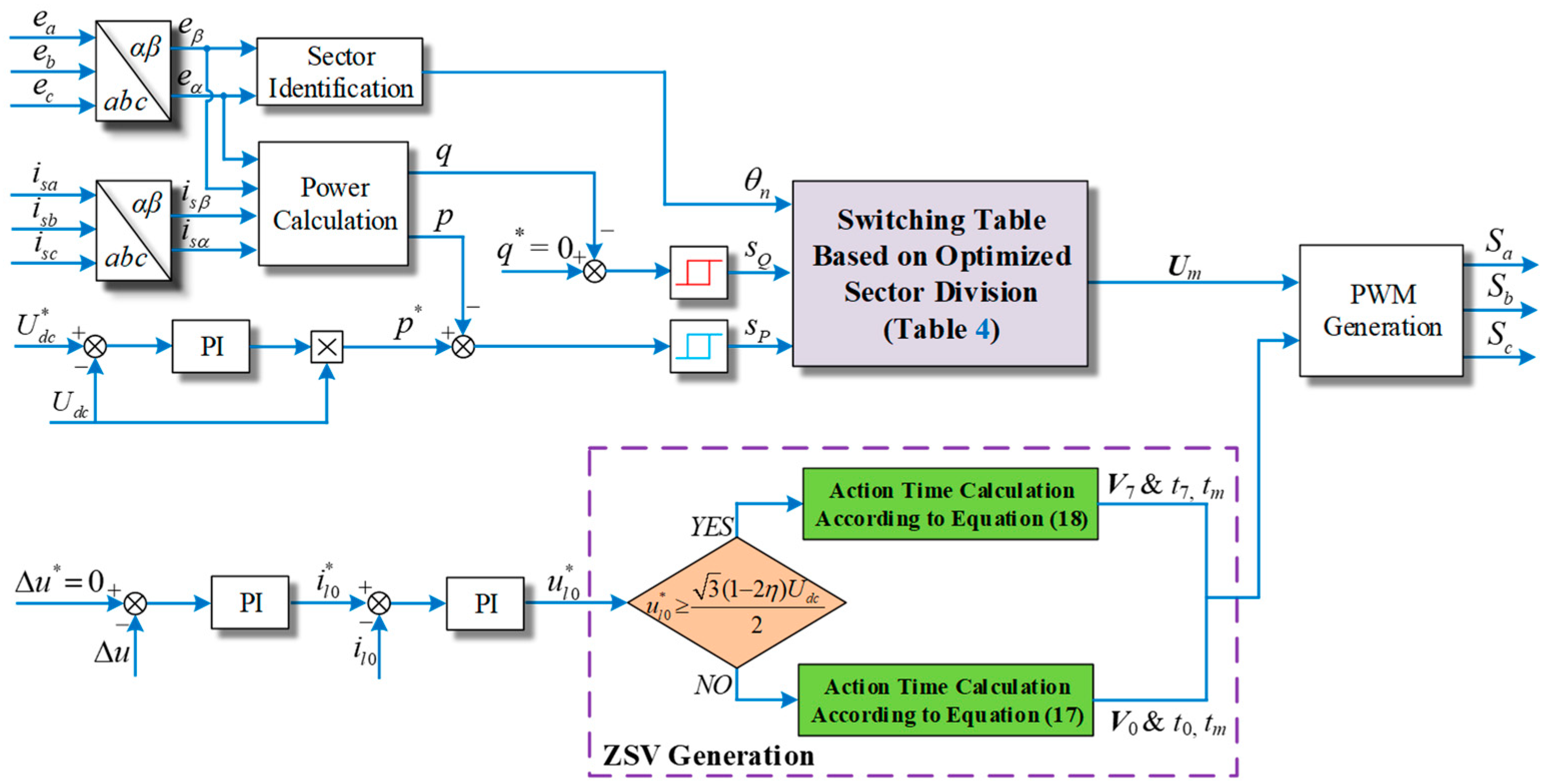
- A set of new voltage vectors are synthesized in the proposed DPC strategy to extend the eight basic voltage vectors. Based on the new synthesized voltage vectors, the zero-sequence current in TCI can be controlled in a stable manner while implementing the hysteresis power control of the TCIBAR.
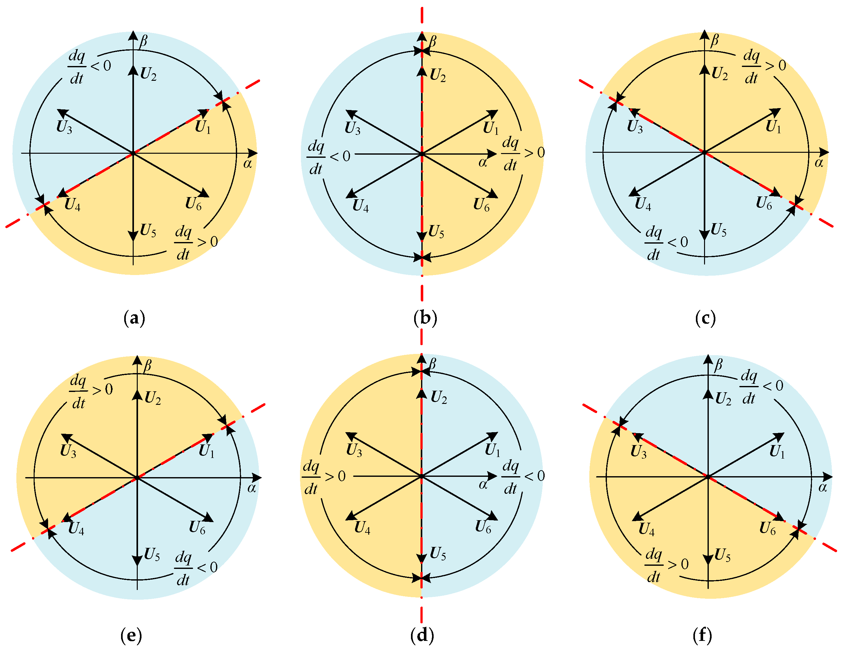
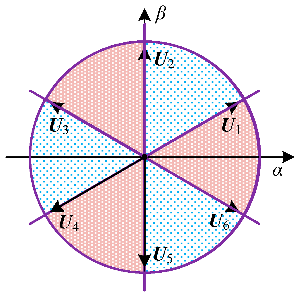
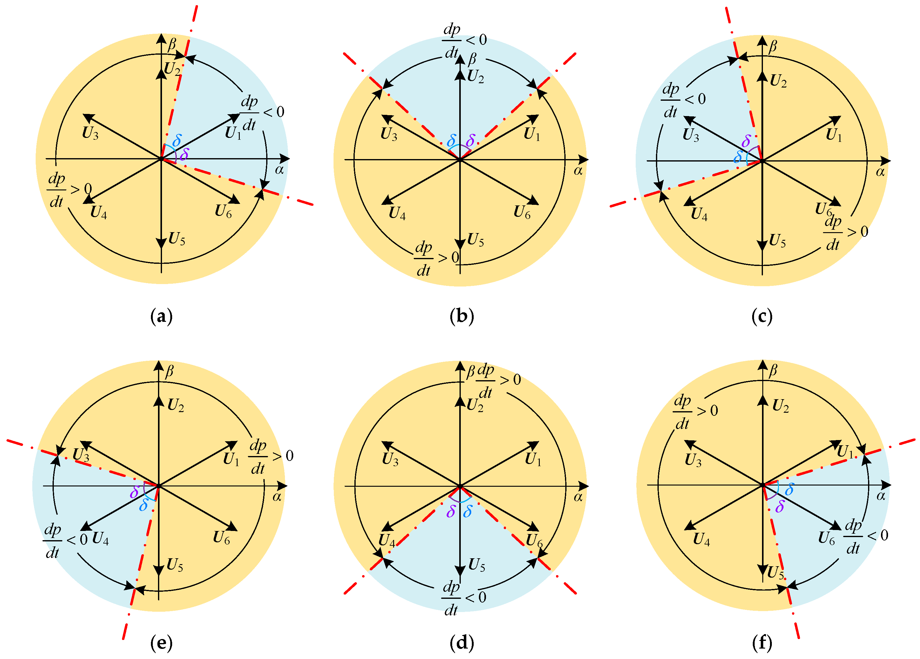
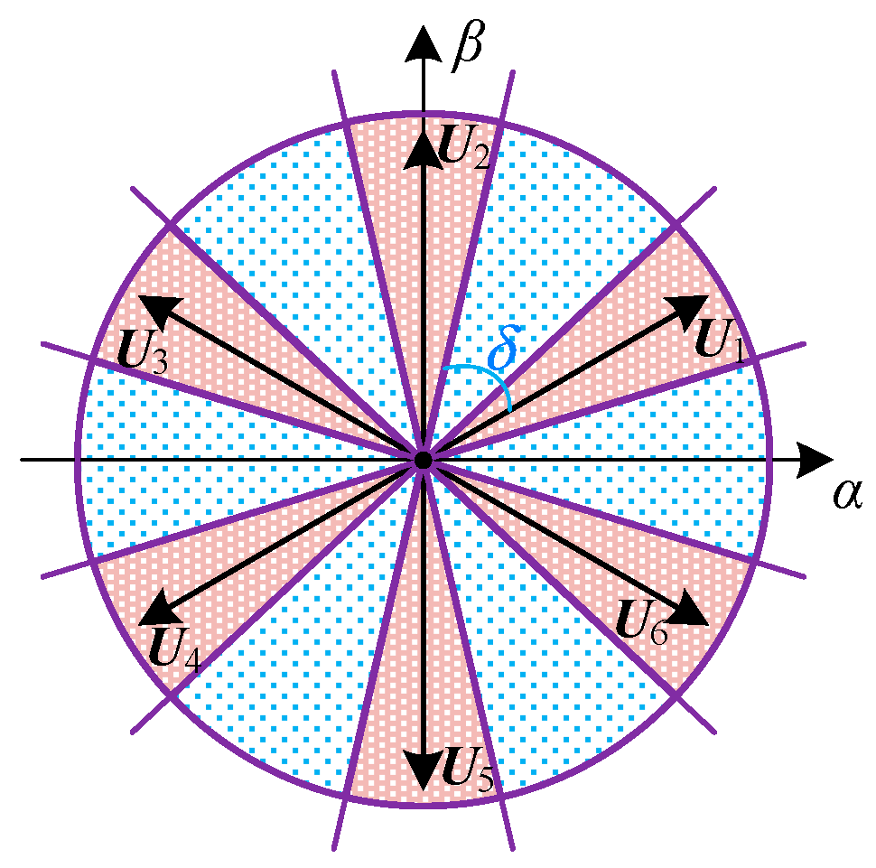
- Based on the derived power model of TCIBAR in the synchronous rotating coordinate system, the effect of the new synthesized voltage vectors on the power variation of TCIBAR is quantitatively analyzed. On this basis, an optimized sector division method is proposed to establish a new switching table for TCIBAR, which can improve the quality of the phase currents in TCIBAR.
- A ZSV generation method is developed in the proposed DPC strategy. Based on the ZSV generation method, the voltage balance control of the bipolar DC ports in TCIBAR can be realized, even under unbalanced load conditions.
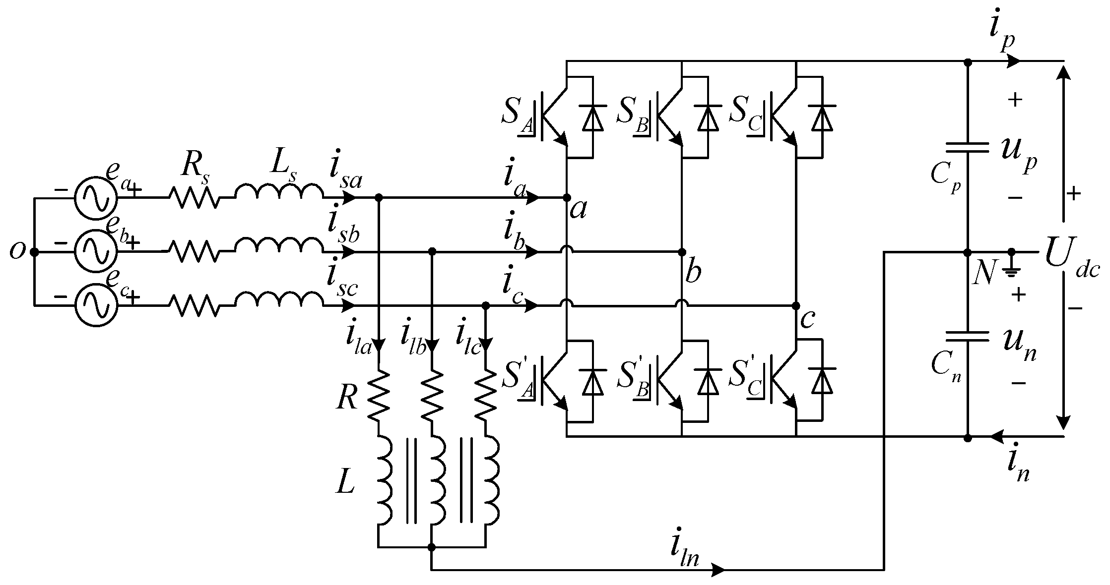
2. TCIBAR Model Based on Instantaneous Power Theory
3. Proposed DPC Based on Optimized Sector Division
3.1. Extension of Voltage Vector
3.2. Effect of Voltage Vector on Power Variation
3.2.1. Vector Space Division for Reactive Power
3.2.2. Vector Space Division for Active Power
3.3. Optimized Sector Division and Switching Table
3.4. Voltage Balance Control under DPC Architecture
4. Experimental Results
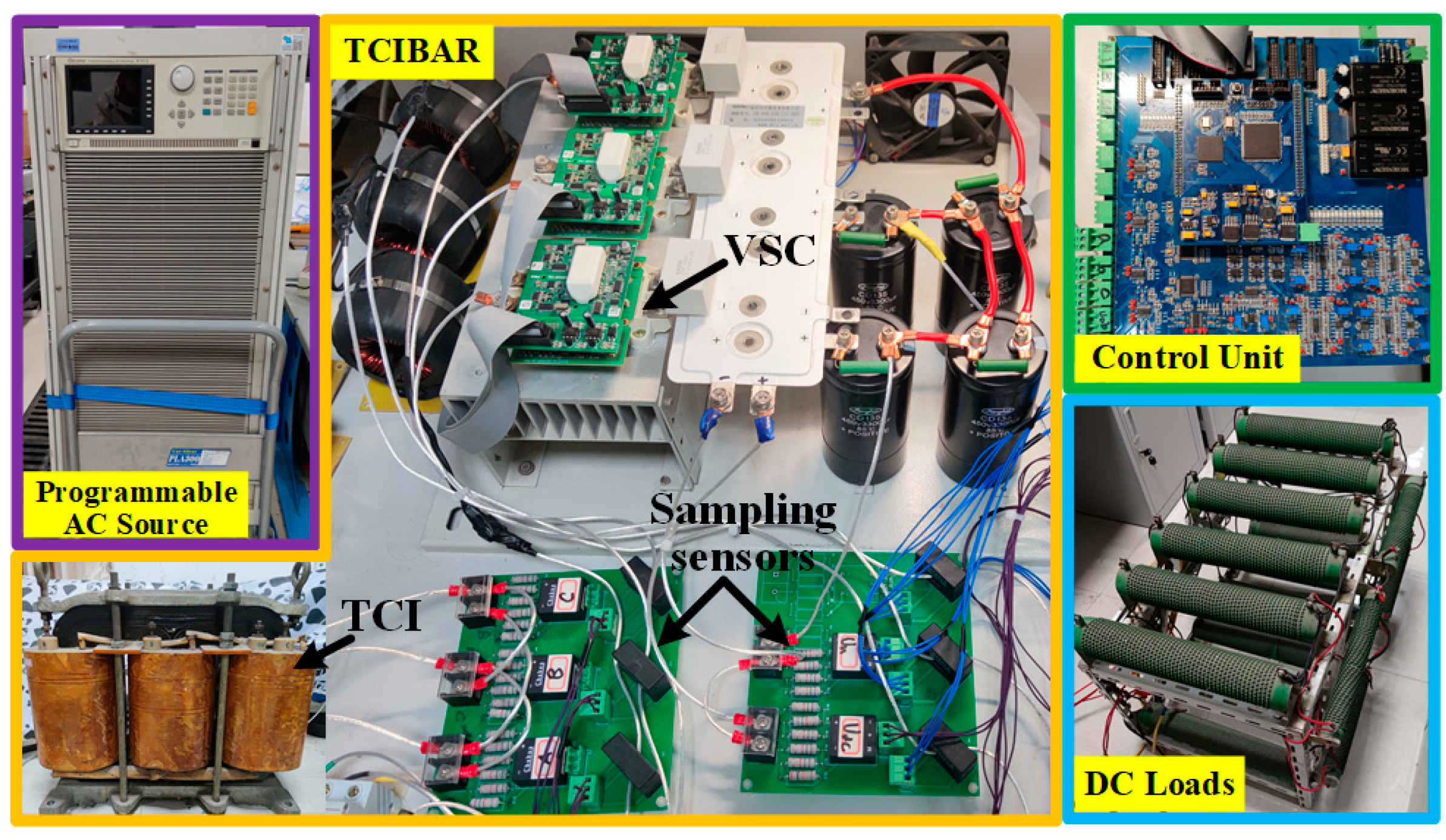
4.1. Experimental Parameters
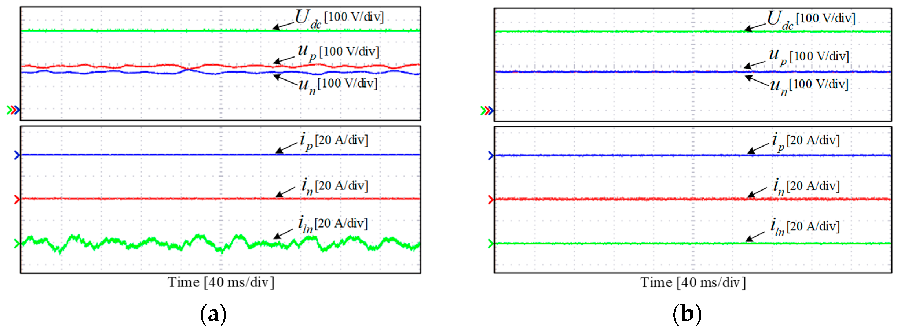
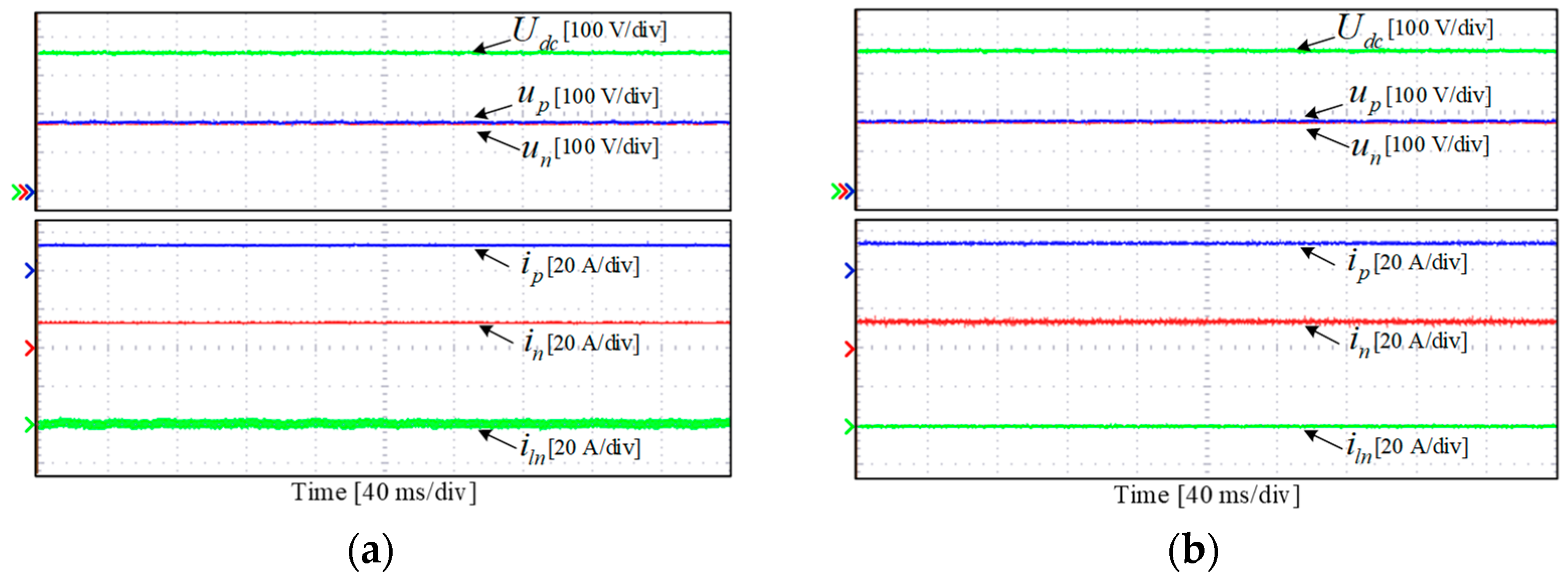
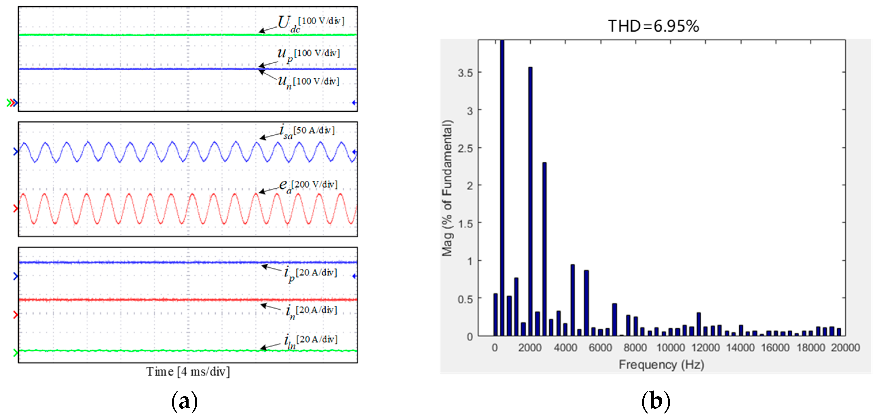
4.2. Steady State Experimental Study
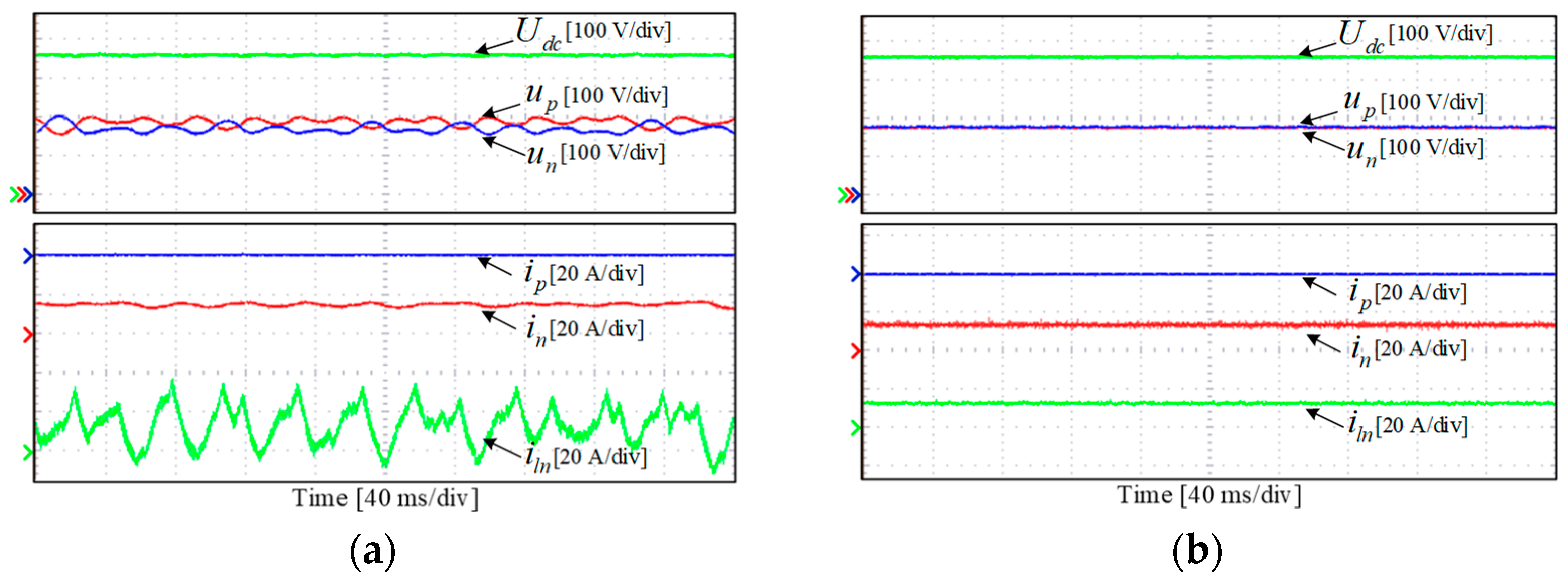
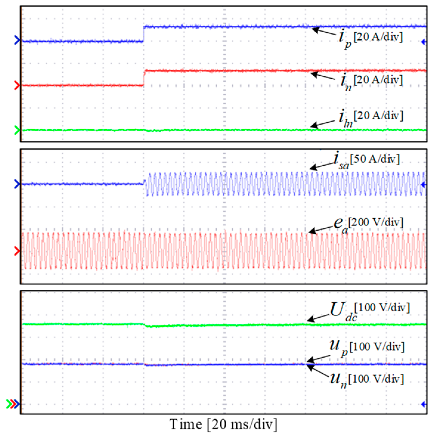
4.3. Dynamic Experimental Study
5. Conclusions
- Based on the instantaneous power theory, the power model of the TCIBAR in the synchronous rotating coordinate system was established and verified.
- Based on the new synthesized voltage vectors, the proposed DPC strategy realized the hysteresis power control of TCIBAR without causing the runaway of the zero-sequence current in TCI.
- The optimized sector division method in the proposed DPC strategy effectively reduced the THD of the phase currents and improved the steady-state performance of the TCIBAR.
- Based on the proposed ZSV generation method, the proposed DPC strategy realized the voltage balance control of the bipolar DC ports in TCIBAR and maintained the voltage balance between the bipolar DC ports, even under unbalanced load conditions.
Author Contributions
Funding
Data Availability Statement
Conflicts of Interest
Abbreviations
| DPC | Direct power control |
| MEA | More electric aircraft |
| TCIBAR | Three-phase coupled inductor-based bipolar output active rectifier |
| TCI | Three-phase coupled inductor |
| ZSV | Zero-sequence voltage |
| EPS | Electrical power system |
| HVDC | High-voltage direct current |
| ATRU | Auto transformer rectifier unit |
| VSC | Voltage source converter |
| VOC | Voltage-oriented control |
| PI | Proportional–integral |
| FFT | Fast Fourier transform |
| THD | Total harmonic distortion |
References
- Barzkar, A.; Ghassemi, M. Electric power systems in more and all electric aircraft: A review. IEEE Access 2020, 8, 169314–169332. [Google Scholar] [CrossRef]
- Sayed, E.; Abdalmagid, M.; Pietrini, G.; Sa’adeh, N.M.; Callegaro, A.D.; Goldstein, C.; Emadi, A. Review of electric machines in more-/hybrid-/turbo-electric aircraft. IEEE Trans. Transp. Electrif. 2021, 7, 2976–3005. [Google Scholar] [CrossRef]
- Weng, L.; Zhang, X.; Yao, T.; Bu, F.; Li, H. A thrust cooperative control strategy of multiple propulsion motors for distributed electric propulsion aircraft. World Electr. Veh. J. 2021, 12, 199. [Google Scholar] [CrossRef]
- Rajashekara, K. Power conversion technologies for automotive and aircraft systems. IEEE Electrif. Mag. 2014, 2, 50–60. [Google Scholar] [CrossRef]
- Chen, W.; Li, S.; Sun, W.; Bi, K.; Lin, Z.; Zhang, G. Wide frequency PWM rectifier control system based on improved deadbeat direct power control. World Electr. Veh. J. 2022, 13, 230. [Google Scholar] [CrossRef]
- Patnaik, B.; Kumar, S.; Gawre, S. Recent advances in converters and storage technologies for more electric aircrafts: A review. IEEE J. Miniat. Air Space Syst. 2022, 3, 78–87. [Google Scholar] [CrossRef]
- Roboam, X.; Sareni, B.; Andrade, A.D. More electricity in the air: Toward optimized electrical networks embedded in more-electrical aircraft. IEEE Ind. Electron. Mag. 2012, 6, 6–17. [Google Scholar] [CrossRef]
- Wheeler, P. Technology for the more and all electric aircraft of the future. In Proceedings of the 2016 IEEE International Conference on Automatica (ICA–ACCA), Curico, Chile, 19–21 October 2016. [Google Scholar]
- Lang, X.; Yang, T.; Enalou, H.B.; Bozhko, S.; Wheeler, P. An enhanced power generation centre for more electric aircraft applications. In Proceedings of the 2018 IEEE International Conference on Electrical Systems for Aircraft, Railway, Ship Propulsion and Road Vehicles & International Transportation Electrification Conference (ESARS-ITEC), Nottingham, UK, 7–9 November 2018. [Google Scholar]
- Sarlioglu, B.; Morris, C.T. More electric aircraft: Review, challenges, and opportunities for commercial transport aircraft. IEEE Trans. Transp. Electrif. 2015, 1, 54–64. [Google Scholar] [CrossRef]
- Schefer, H.; Fauth, L.; Kopp, T.H.; Mallwitz, R.; Friebe, J.; Kurrat, M. Discussion on electric power supply systems for all electric aircraft. IEEE Access 2020, 8, 84188–84216. [Google Scholar] [CrossRef]
- Chen, J.W.; Wang, C.; Chen, J. Investigation on the selection of electric power system architecture for future more electric aircraft. IEEE Trans. Transp. Electrif. 2018, 4, 563–576. [Google Scholar] [CrossRef]
- Lei, T.; Min, Z.; Gao, Q.; Song, L.; Zhang, X.; Zhang, X. The architecture optimization and energy management technology of aircraft power systems: A review and future trends. Energies 2022, 15, 4109. [Google Scholar] [CrossRef]
- Madonna, V.; Giangrande, P.; Galea, M. Electrical power generation in aircraft: Review, challenges, and opportunities. IEEE Trans. Transp. Electrif. 2018, 4, 646–659. [Google Scholar] [CrossRef]
- Karanayil, B.; Ciobotaru, M.; Agelidis, V.G. Power flow management of isolated multiport converter for more electric aircraft. IEEE Trans. Power Electron. 2017, 32, 5850–5861. [Google Scholar] [CrossRef]
- Buticchi, G.; Bozhko, S.; Liserre, M.; Wheeler, P.; Al-Haddad, K. On-board microgrids for the more electric aircraft–Technology review. IEEE Trans. Ind. Electron. 2019, 66, 5588–5599. [Google Scholar] [CrossRef]
- Yang, T.; Bozhko, S.; Wheeler, P.; Wang, S.; Wu, S. Generic functional modelling of multi-pulse auto-transformer rectifier units for more-electric aircraft applications. Chin. J. Aeronaut. 2018, 31, 883–891. [Google Scholar] [CrossRef]
- Chen, J.; Shen, J.; Chen, J.; Shen, P.; Song, Q.; Gong, C. Investigation on the selection and design of step-up/down 18-pulse ATRUs for more electric aircrafts. IEEE Trans. Transp. Electrif. 2019, 5, 795–811. [Google Scholar] [CrossRef]
- Yang, T.; Bozhko, S.; Asher, G. Functional modeling of symmetrical multipulse autotransformer rectifier units for aerospace application. IEEE Trans. Power Electron. 2015, 30, 4704–4713. [Google Scholar] [CrossRef]
- Zhao, Y.; Huang, W.; Bu, F. DC voltage balancing strategy of a bipolar-output active rectifier for more electric aircraft based on zero vector redistribution. IEEE Access 2021, 9, 139657–139667. [Google Scholar] [CrossRef]
- Li, Y.; Junyent-Ferre, A.; Rodriguez-Bernuz, J.M. A three-phase active rectifier topology for bipolar dc distribution. IEEE Trans. Power Electron. 2018, 33, 1063–1074. [Google Scholar] [CrossRef]
- Rivera, S.; Lizana, R.; Kouro, S.; Dragicevic, T.; Wu, B. Bipolar dc power conversion: State-of-the-art and emerging technologies. IEEE J. Emerg. Sel. Top. Power Electron. 2021, 9, 1192–1204. [Google Scholar] [CrossRef]
- Yan, S.; Yang, Y.; Hui, S.Y.; Blaabjerg, F. A review on direct power control of pulsewidth modulation converters. IEEE Trans. Power Electron. 2021, 36, 11984–12007. [Google Scholar] [CrossRef]
- Zhang, Y.; Jiao, J.; Liu, J.; Gao, J. Direct power control of PWM rectifier with feedforward compensation of DC-bus voltage ripple under unbalanced grid conditions. IEEE Trans. Ind. Appl. 2019, 55, 2890–2901. [Google Scholar] [CrossRef]
- Noguchi, T.; Tomiki, H.; Kondo, S.; Takahashi, I. Direct power control of PWM converter without power-source voltage sensors. IEEE Trans. Ind. Appl. 1998, 34, 473–479. [Google Scholar] [CrossRef]
- Zhang, Y.; Gao, J.; Qu, C. Relationship between two direct power control methods for PWM rectifiers under unbalanced network. IEEE Trans. Power Electron. 2017, 32, 4084–4094. [Google Scholar] [CrossRef]
- Sato, A.; Noguchi, T. Voltage-source PWM rectifier–inverter based on direct power control and its operation characteristics. IEEE Trans. Power Electron. 2011, 26, 1559–1567. [Google Scholar] [CrossRef]
- Yan, S.; Chen, J.; Yang, T.; Hui, S.Y. Improving the performance of direct power control using duty cycle optimization. IEEE Trans. Power Electron. 2019, 34, 9213–9223. [Google Scholar] [CrossRef]
- Zhang, Y.; Qu, C.; Gao, J. Performance improvement of direct power control of PWM rectifier under unbalanced network. IEEE Trans. Power Electron. 2017, 32, 2319–2328. [Google Scholar] [CrossRef]
- Zhang, Y.; Qu, C. Table-based direct power control for three-phase AC/DC converters under unbalanced grid voltages. IEEE Trans. Power Electron. 2015, 30, 7090–7099. [Google Scholar] [CrossRef]
- Hamed, H.A.; Abdou, A.F.; Acharya, S.; El Moursi, M.S.; EL-Kholy, E.E. A novel dynamic switching table based direct power control strategy for grid connected converters. IEEE Trans. Energy Convers. 2018, 33, 1086–1097. [Google Scholar] [CrossRef]
- Huang, J.; Guo, F.; Wen, C.; Yang, B.; Xiao, J. A direct power control strategy for AC/DC converter based on best switching state approach. IEEE J. Emerg. Sel. Top. Power Electron. 2018, 6, 2273–2286. [Google Scholar] [CrossRef]
- Eloy-Garcia, J.; Alves, R. DSP-based direct power control of a VSC with voltage angle estimation. In Proceedings of the 2006 IEEE/PES Transmission & Distribution Conference and Exposition: Latin America, Caracas, Venezuela, 15–18 August 2006. [Google Scholar]
- Chen, B.S.; Joos, G. Direct power control of active filters with averaged switching frequency regulation. IEEE Trans. Power Electron. 2008, 23, 2729–2737. [Google Scholar] [CrossRef]



| Vectors | Sa | Sb | Sc | Sd | Sq | S0 |
|---|---|---|---|---|---|---|
| V0 | 0 | 0 | 0 | |||
| V1 | 1 | 0 | 0 | |||
| V2 | 1 | 1 | 0 | |||
| V3 | 0 | 1 | 0 | |||
| V4 | 0 | 1 | 1 | |||
| V5 | 0 | 0 | 1 | |||
| V6 | 1 | 0 | 1 | |||
| V7 | 1 | 1 | 1 |
| Vectors | Sa | Sb | Sc | Sd | Sq | S0 |
|---|---|---|---|---|---|---|
| U1 | 1 | 0.5 | 0 | |||
| U2 | 0.5 | 1 | 0 | |||
| U3 | 0 | 1 | 0.5 | |||
| U4 | 0 | 0.5 | 1 | |||
| U5 | 0.5 | 0 | 1 | |||
| U6 | 1 | 0 | 0.5 |
| sP | sQ | θ1 | θ2 | θ3 | θ4 | θ5 | θ6 | θ7 | θ8 | θ9 | θ10 | θ11 | θ12 |
|---|---|---|---|---|---|---|---|---|---|---|---|---|---|
| 0 | 0 | U6 | U6 | U1 | U1 | U2 | U2 | U3 | U3 | U4 | U4 | U5 | U5 |
| 0 | 1 | U1 | U1 | U2 | U2 | U3 | U3 | U4 | U4 | U5 | U5 | U6 | U6 |
| 1 | 0 | U4 | U5 | U5 | U6 | U6 | U1 | U1 | U2 | U2 | U3 | U3 | U4 |
| 1 | 1 | U2 | U3 | U3 | U4 | U4 | U5 | U5 | U6 | U6 | U1 | U1 | U2 |
| sP | sQ | θ1 | θ2 | θ3 | θ4 | θ5 | θ6 | θ7 | θ8 | θ9 | θ10 | θ11 | θ12 | θ13 | θ14 | θ15 | θ16 | θ17 | θ18 |
|---|---|---|---|---|---|---|---|---|---|---|---|---|---|---|---|---|---|---|---|
| 0 | 0 | U6 | U6 | U6 | U1 | U1 | U1 | U2 | U2 | U2 | U3 | U3 | U3 | U4 | U4 | U4 | U5 | U5 | U5 |
| 0 | 1 | U1 | U1 | U1 | U2 | U2 | U2 | U3 | U3 | U3 | U4 | U4 | U4 | U5 | U5 | U5 | U6 | U6 | U6 |
| 1 | 0 | U5 | U5 | U6 | U6 | U6 | U1 | U1 | U1 | U2 | U2 | U2 | U3 | U3 | U3 | U4 | U4 | U4 | U5 |
| 1 | 1 | U1 | U2 | U2 | U2 | U3 | U3 | U3 | U4 | U4 | U4 | U5 | U5 | U5 | U6 | U6 | U6 | U1 | U1 |
| Parameter | Symbol | Value |
|---|---|---|
| Rated power | P | 5 kW |
| RMS value of AC source phase voltage | Eac | 115 V |
| Frequency of AC source | fac | 400 Hz |
| Rated DC bus voltage | Udc | 360 V |
| Rated positive voltage | up | 180 V |
| Rated negative voltage | un | 180 V |
| Positive port capacitance | Cp | 6600 μF |
| Negative port capacitance | Cn | 6600 μF |
| Filter inductance | Ls | 1.5 mH |
| Self-inductance of TCI | L | 0.526 H |
| Mutual inductance of TCI | M | 0.259 H |
Disclaimer/Publisher’s Note: The statements, opinions and data contained in all publications are solely those of the individual author(s) and contributor(s) and not of MDPI and/or the editor(s). MDPI and/or the editor(s) disclaim responsibility for any injury to people or property resulting from any ideas, methods, instructions or products referred to in the content. |
© 2023 by the authors. Licensee MDPI, Basel, Switzerland. This article is an open access article distributed under the terms and conditions of the Creative Commons Attribution (CC BY) license (https://creativecommons.org/licenses/by/4.0/).
Share and Cite
Zhao, Y.; Huang, W.; Bu, F. Direct Power Control of a Bipolar Output Active Rectifier for More Electric Aircraft Based on an Optimized Sector Division. World Electr. Veh. J. 2023, 14, 89. https://doi.org/10.3390/wevj14040089
Zhao Y, Huang W, Bu F. Direct Power Control of a Bipolar Output Active Rectifier for More Electric Aircraft Based on an Optimized Sector Division. World Electric Vehicle Journal. 2023; 14(4):89. https://doi.org/10.3390/wevj14040089
Chicago/Turabian StyleZhao, Yajun, Wenxin Huang, and Feifei Bu. 2023. "Direct Power Control of a Bipolar Output Active Rectifier for More Electric Aircraft Based on an Optimized Sector Division" World Electric Vehicle Journal 14, no. 4: 89. https://doi.org/10.3390/wevj14040089
APA StyleZhao, Y., Huang, W., & Bu, F. (2023). Direct Power Control of a Bipolar Output Active Rectifier for More Electric Aircraft Based on an Optimized Sector Division. World Electric Vehicle Journal, 14(4), 89. https://doi.org/10.3390/wevj14040089


