Article

Research on Cascaded Single Phase PFC Based on Predictive PI Control

College of Mechanical and Electrical Engineering, Chizhou University, Chizhou 247000, China
*
Author to whom correspondence should be addressed.
World Electr. Veh. J. 2022, 13(3), 48; https://doi.org/10.3390/wevj13030048
Submission received: 22 January 2022 / Revised: 23 February 2022 / Accepted: 25 February 2022 / Published: 2 March 2022

Abstract

:
In order to improve the charging speed and reduce the occupied volume of an electric vehicle charger, a single-phase boost power factor corrector (PFC) system with cascade CHB (cascaded H-bridge) topology was adopted. Due to the periodic fluctuation of single-phase AC input, there is a large double power frequency ripple component in the output voltage of an AC-DC converter. When capacitor voltage is used as output for feedback control, the control system has the characteristics of a non-minimum phase system. In light of these factors that affect the dynamic stability of the system, a control method is proposed to improve the dynamic characteristics of the system without affecting its steady-state performance. The predictive PI control strategy was adopted to predict the error input signal of the lag process to attenuate the jitter in the control system and improve the dynamic performance and anti-interference of the system. Finally, the feasibility of the scheme was verified by experiments.

1. Introduction

With the rapid development of the electric vehicle industry, the charging speed and convenience of electric vehicles have been put forward as having higher requirements. Electric vehicle charging can be divided into DC charging and AC charging. DC charging charges the battery by the public fast charging pile, which is fast but inconvenient; AC charging charges the vehicle power battery indirectly, when the AC current is converted by the on-board charger. It can be charged in private places and is more popular with ordinary consumers [1]. Generally, the three-phase circuit is used in high-power occasions (such as charging pile, etc.). In daily life, the most common power distribution mode is single-phase electricity, so the power supply mode of a vehicle charger mostly adopts single-phase AC power supply. The main circuit converter designed in this project adopted the single-phase AC-DC structure. However, the charging speed is limited due to the small charging power. If the charging power of on-board charger is increased, it will be restricted by the space of the electric vehicle itself. The inductor volume accounts for about 36% of the total PFC volume [2]. The inductor volume depends on the inductor volume and peak current, and the inductor volume is determined by its volt-second [3]. The inductance can be reduced by increasing the switching frequency of the system and reducing the voltage at both ends of the inductor to reduce the volume of the inductor. The cascaded H-bridge converter increases the number of levels to reduce the voltage at both ends of the inductor, and the carrier phase-shift modulation can greatly increase the frequency of the inductor current [4,5]. With the increase in the number of levels, the inductance volume gradually decreases. When it increases from three levels to eleven levels, the inductance volume can be reduced by about 90% [6]. Therefore, the single-phase AC-DC converter designed in this project adopted cascade structure and carrier phase shift modulation.
Due to the periodic pulsation of single-phase AC input, the output voltage of the AC-DC converter will inevitably have a large double power frequency ripple component. The second harmonic component of the output voltage is fed back to the outer voltage loop, resulting in the distortion of the reference current generated by the output signal of the compensator, and the third harmonic current will be generated in the AC side. Therefore, the bandwidth of the voltage loop is usually limited to a frequency much lower than the ripple frequency to avoid the input current waveform distortion caused by the fast response speed of the voltage loop and the fast change of the turn-on time. For the application where the load is basically stable, the lower voltage loop bandwidth can meet the system requirements. However, in the application where the load is often changing rapidly, the circuit response speed is slow, and the interference will lead to the voltage fluctuation of the output DC bus, which will cause additional pressure on the devices in the system. This not only reduces the control performance of the system, but also does harm to the load [7,8]. In addition, the voltage power level transfer function of the AC-DC converter is the transfer function of non-minimum phase system, so it is necessary to suppress the negative regulation caused by unstable zero and shorten the regulation time of the system [9]. Therefore, it is of great significance to reduce the overshoot and adjustment time and improve the dynamic response ability of the system.
In order to ensure high-quality input current waveform control and effectively improve the dynamic performance of a single-phase AC-DC converter, some scholars have eliminated the ripple component of DC output voltage from the hardware level of the main circuit. A passive scheme is adopted, in which the LC resonant branch is paralleled on the DC output bus of a single-phase AC-DC converter to bypass the second harmonic current at the output [10]. The main circuit is embedded with a branch especially used to buffer the instantaneous power difference to balance the instantaneous power between the input and output [11]. An active energy storage unit is paralleled on the DC output bus to filter the second harmonic current at the output [12]. The methods described above all increase passive components, while inductance or capacitance will make the circuit order higher and robustness lower, which makes the analysis more complicated.
Some scholars have used the load dynamic information feedforward method to improve the system dynamic response speed. Effective feedforward schemes include load current feedforward, DC output voltage ripple feedforward and load power feedforward, etc. In [13], the load current feedforward is introduced to counteract the influence of load disturbance on the control system. On the basis of average current control, an improved double feedforward control including input and load feedforward was proposed in [14] to optimize the dynamic response of the system, and the peak voltage prediction was used to further improve the performance of the control. A real-time load prediction voltage loop output was proposed, and then the duty cycle was calculated directly from the voltage loop output in [15]. An adaptive constant power control method, adaptive constant power angle operation, has been proposed to achieve efficiency control under light load, while still meeting the output voltage requirements [16]. A comprehensive sliding mode control method was proposed to improve the dynamic performance of the converter and ensure the unity power factor by selecting the appropriate sliding surface coefficient [17]. A feed-forward method was proposed to compensate the harmonic distortion of the reference current by introducing the harmonic component of the input current into the control loop [18]. However, the above scheme requires additional sensors or observers to detect the load current or power feedforward signals, which increases the complexity and cost of the system.
In this paper, a cascaded multilevel PFC scheme was proposed, which will effectively improve the power density of the system. The flying capacitor multilevel circuit with carrier phase-shifting modulation not only increases the frequency of the inductor current, but also decreases the maximum voltage at both ends of the inductor. The predictive PI control algorithm was proposed to improve the dynamic performance of the single-phase cascade PFC system. Facing the problem of a non-minimum phase system in voltage loop, the predictive PI control strategy was used to predict the error input signal of the delay process to attenuate the jitter in the control system and improve the dynamic performance and anti-interference of the system.
The rest of this paper is organized as follows. Section 1 reports the existing works of cascaded single phase PFC. Section 2 introduces the structure of a cascaded single phase PFC system. Section 3 details the design of cascade single phase PFC control system. Section 4 details the system experimental analysis. Finally, Section 5 presents the conclusions of this paper.

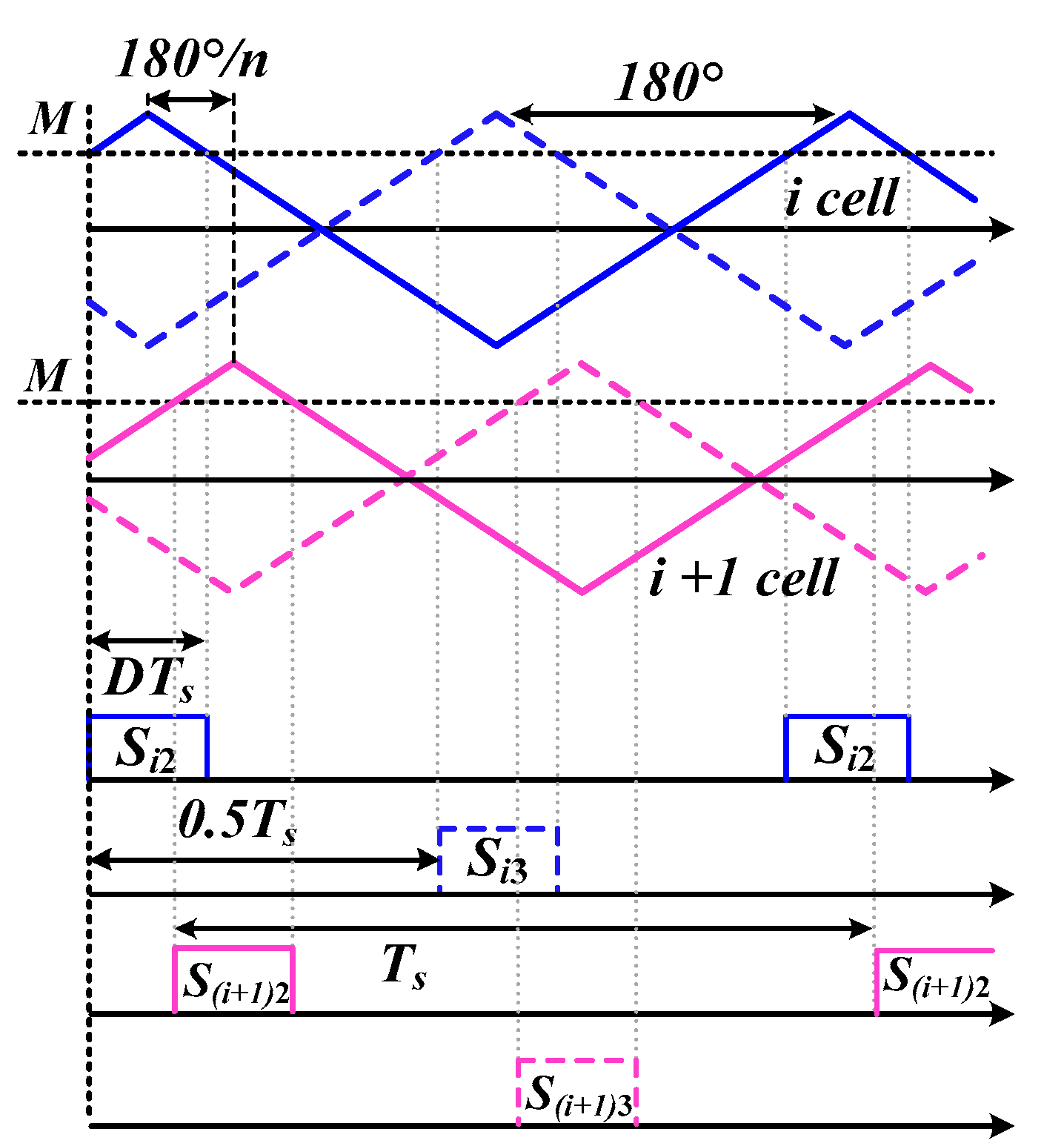
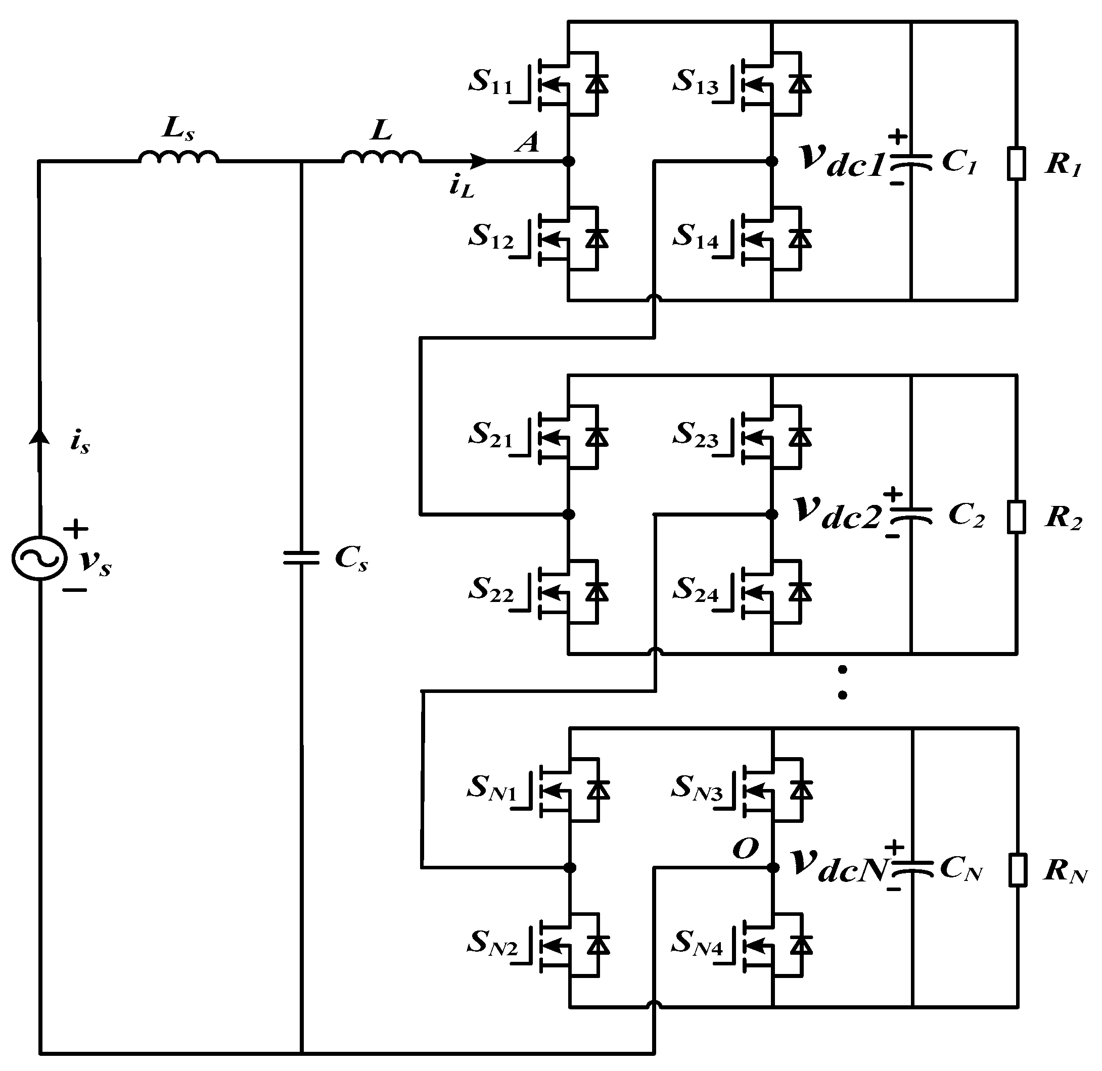
2. Structure of Cascaded Single Phase PFC System

Figure 1 shows the topology of a single-phase N-unit cascaded PFC, which is composed of N H-bridge units in series. On the AC side, vs. is the grid voltage, is is the AC side current, Ls is the filter inductor, Cs is the filter capacitor, L is the boost inductor, and iL is the current flowing through the inductor L. Ci and Ri (i = 1, 2 … N) are the capacitors and DC loads. On the DC side, vdc1, vdc2vdcN are the voltages across the capacitors’ side of the H-bridge. The DC load Ri is used to replace the PFC post stage converter, where i is the serial connection unit number.
For the convenience of analysis, the following assumptions can be made:
(1)
The common duty cycle control strategy is adopted, and the difference of switching function caused by CPS-SPWM is ignored, that is, m1m2 ≈ … ≈ mi; and
(2)
The capacitance and resistance of the DC side are the same, which are C and R, respectively.
The modulation waveforms of unit i and unit i + 1 are shown in Figure 2. For the CHB of N units, the carrier phase difference between the left and right bridge arms of each unit is 180°, and the carrier phase difference between the bridge arms of adjacent units is 180°/n,
By using Kirchhoff’s law of voltage and current, the following relation can be obtained as Equation (1):
{ L d i L d t = v s i = 1 N m v d c i ( i = 1 N ) C d v d c i d t = m i L v d c i R ( i = 1 N )
where m = vs/Nvdc, vdc = vdc1 = vdc2 ⋯ = vdcN.
On the basis of this large signal, small signal disturbance was added, as shown in Equation (2).
{ v i n = V i n + v ^ i n i i n = I i n + i ^ i n v d c j = V d c j + v ^ d c j M = M + m ^
The disturbance is substituted into the large signal and Laplace transform is performed as Equation (3):
{ s L v ^ i n i ^ L ( s ) = v ^ s ( s ) N V d c m ^ ( s ) M i = 1 N V d c i ( s ) s C V d c i ( s ) = I L m ^ ( s ) + M i ^ L ( s ) 1 R V d c i ( s ) ( i = 1 N )
By eliminating the DC component and ignoring the second-order small signal component, the small signal power stage transfer function of a single-phase cascaded PFC converter can be obtained.
The transfer function of grid current relative to duty cycle is as follows:
G i m ( s ) = N R C V d c s + 2 N V d c R L C s 2 + L s + M 3 N R
The transfer function of bus voltage relative to duty cycle is as follows:
G v m ( s ) = L V d c s + M 2 N R V d c M R L C s 2 + M L s + M 3 N R
It can be seen from (5) that the transfer function is the transfer function of a non-minimum phase system, and its open-loop step curve has negative modulation at the beginning. The system has a zero point in the right half plane, which will deteriorate the dynamic quality of the control system and lead to a longer transition time of the system. Moreover, in the negative regulation period, the controller receives the opposite feedback signal, forming a positive feedback system and affecting the steady-state performance of the system.

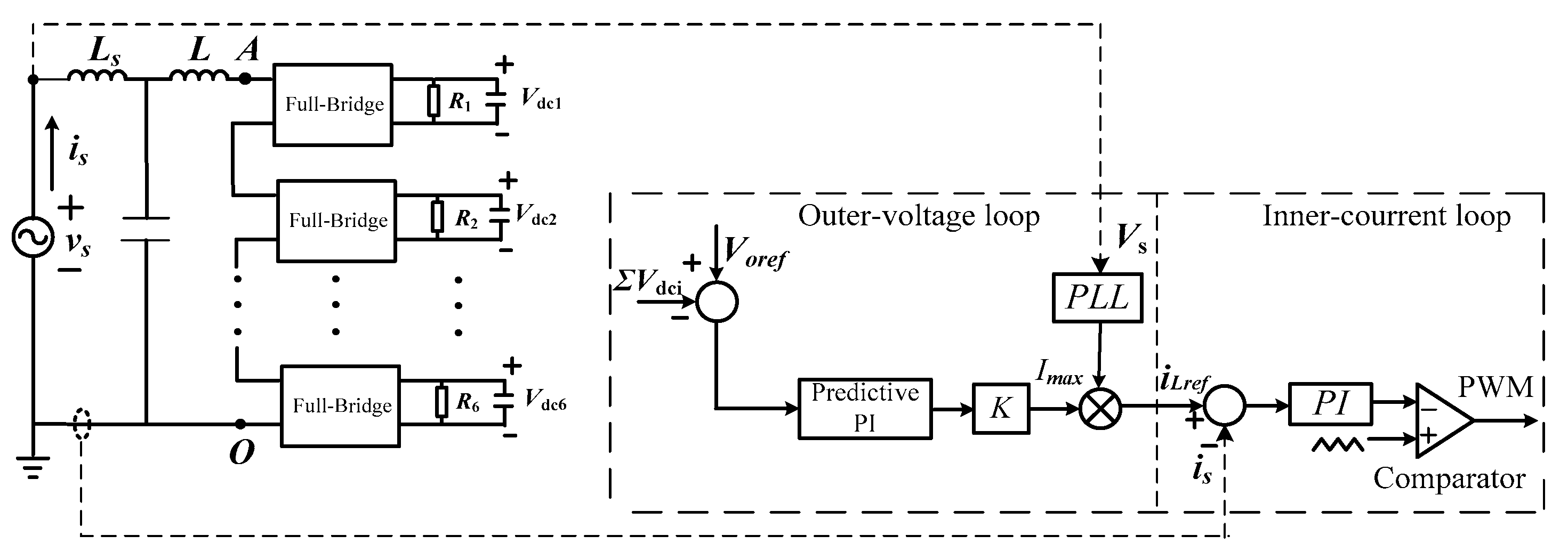
3. Design of Cascade Single Phase PFC Control System

The second harmonic component exists in the output voltage of the AC-DC converter in a single-phase cascaded PFC system, which limits the bandwidth frequency of voltage loop. The voltage power level transfer function of the AC-DC converter is the transfer function of a non-minimum phase system, which affects the dynamic stability of the system. Aiming at the nonlinear characteristics of the above single-phase cascaded PFC system, this paper adopts the double loop control of the voltage outer loop and current inner loop. In the voltage outer loop, predictive PI control was used to improve the dynamic performance of the system. The inner current loop adopts the proportional integral control with simple structure, which not only does not affect the control effect, but also simplifies the control method [19,20]. The schematic diagram of predictive PI control is shown in Figure 3.
According to Figure 3, in the external voltage loop of a single-phase cascade PFC circuit control system, the voltage sampling value ΣVdci is the sum of N capacitor voltages. First, the given value of the voltage loop is compared with the average value of the capacitor voltage obtained by sampling, and the voltage error value is used as the input of the second-order notch filter. The secondary voltage ripple is filtered to improve the bandwidth of the voltage loop. The filtered signal is controlled by predictive PI to eliminate the negative modulation and improve the dynamic performance and anti-interference ability of the system. The maximum value of the current reference value of the appreciating inductor is obtained by multiplying the output signal of the predictive PI control by the scale factor. Then, the maximum value is multiplied by the sinusoidal value of the phase information of the power grid voltage processed by the phase locked loop, and the result is taken as the given value of the current loop. The current error is obtained by comparing the collected boost inductor current with the current reference value. The current error is adjusted by the PI controller, and then compared with triangular wave to obtain the control value. The obtained control quantity is input into the DPWM module to generate pulse, which can control the power switch after passing through the driving circuit [21,22].

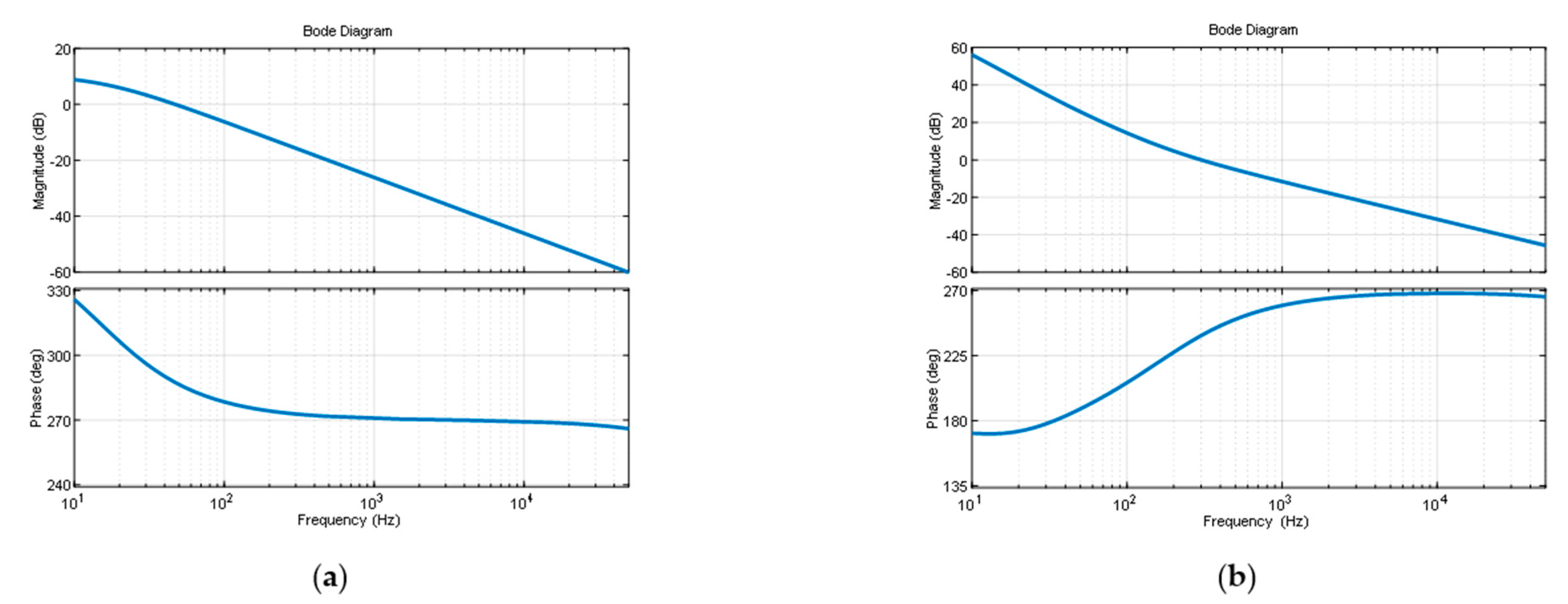
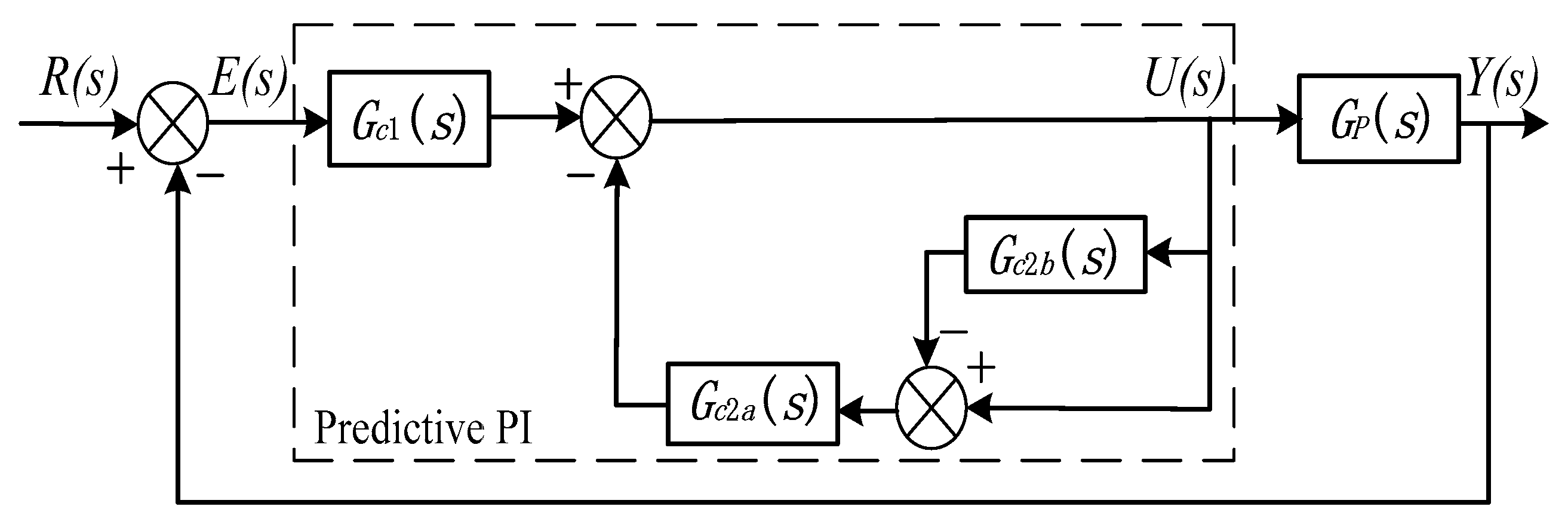
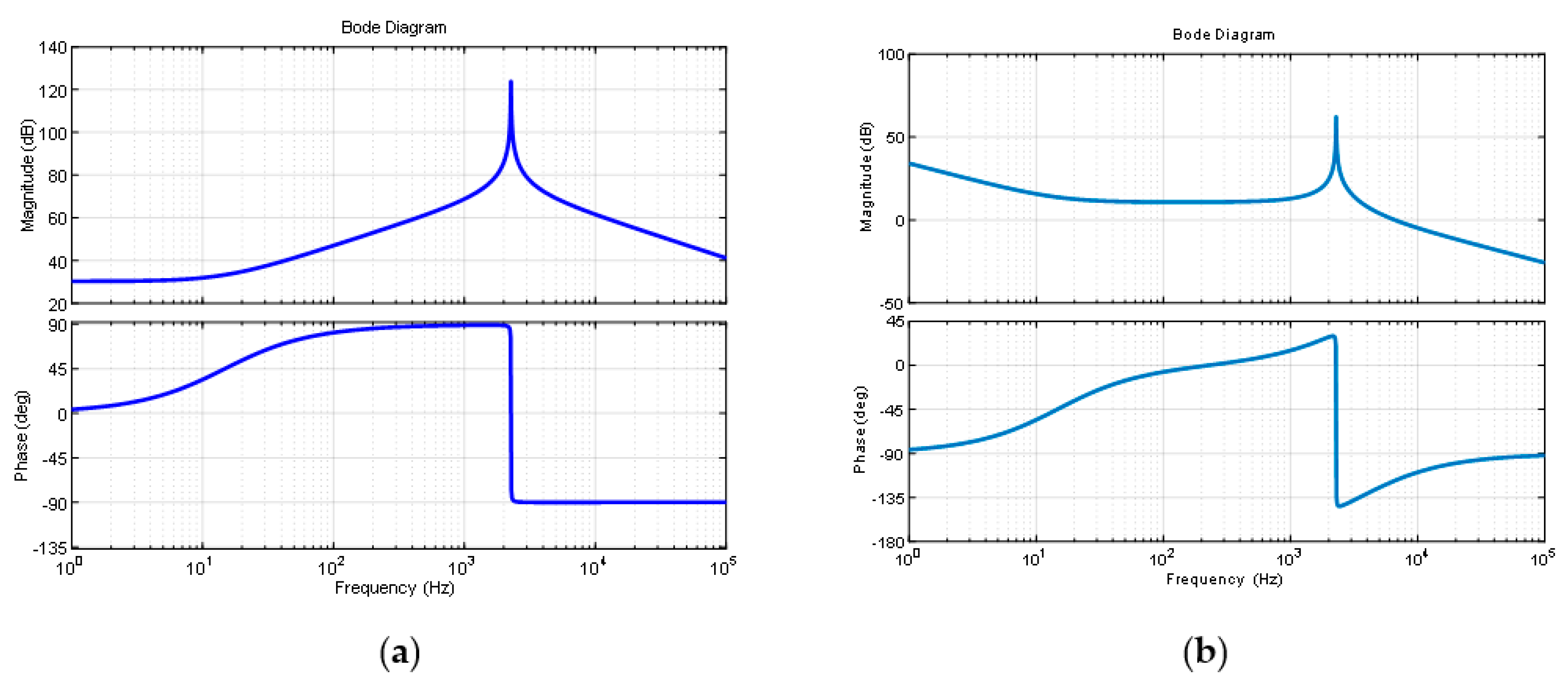
3.1. Predictive PI Control

Since 1992, the idea of predictive PI controller was put forward by Hagland. After step-by-step research and practice, predictive PI control algorithm was successfully applied to complex control systems, especially in the predictive control of multivariable models. This control strategy has a good effect in dealing with feedback mutation and conditional constraints.
The predictive PI control algorithm combines the predictive strategy with the traditional PI control method, and introduces the relevant closed-loop transfer function into the traditional PI control algorithm, so that the whole control strategy not only has the advantages of easy realization of the PI controller, but also has a predictive function. In the face of the first-order inertia lag model, the predictive PI control algorithm can improve the delay of the controlled object and optimize the whole control process effectively. Moreover, the predictive PI controller has excellent robustness and stability. When the actual model parameters of the controlled object change in a certain range, it can also ensure the good performance of the negative feedback system [23,24]. The schematic diagram of predictive PI control is shown in Figure 4.
In Figure 4, E(s) and U(s) are divided into input variables and output variables of the predictive PI controller. The transfer function Gc(s) of the predictive PI controller is composed of Gc1(s) and Gc2(s). Among them, Gc1(s) plays a traditional PI control function, Gc2(s) plays a predictive role, and Gc2(s) is composed of Gc2a(s) and Gc2b(s). GP(s) is the transfer function of the controlled object.
The closed-loop transfer function of the unit negative feedback system is as follows:
G ( s ) = G C ( s ) G P ( s ) 1 + G C ( s ) G P ( s )
Then, the transfer function of the controller is as in Equation (7):
G C ( s ) = G ( s ) G P ( s ) ( 1 G ( s ) )
It is assumed that the mathematical model of the process system object is as follows:
G P ( s ) = K T s + 1 e τ s
The expected closed-loop transfer function is as follows:
G ( s ) = 1 λ T s + 1 e τ s
The predictive PI control algorithm introduces adjustable variable parameters, which can change the real-time response speed of the control system. When λ = 1, the open-loop response time constant of the control system is consistent with the negative feedback closed-loop response time constant. When λ < 1, the response time constant of the negative feedback closed-loop is smaller; when λ > 1, the response time constant of the negative feedback closed-loop is larger.
Substituting Equations (8) and (9) into Equation (7), the transfer function of the controller can be obtained as follows:
G C ( s ) = U ( s ) E ( s ) = G ( s ) G P ( s ) ( 1 G ( s ) ) = 1 + T s K ( 1 + λ T s e τ s )
Equation (10) is transformed into:
U ( s ) = G c 1 ( s ) E ( s ) G c 2 ( s ) U ( s ) = 1 λ k p ( 1 + 1 T s ) E ( s ) 1 λ T s ( 1 e τ s ) U ( s )
From Equation (11), Equations (12) and (13) can be obtained:
G c 1 ( s ) = 1 λ k p ( 1 + 1 T s )
G c 2 ( s ) = G c 2 a ( s ) ( 1 G c 2 b ( s ) ) = 1 λ T s ( 1 e τ s )
Gc1(s) is a traditional PI controller, which is the main control part of the predictive PI control strategy. In a certain range, Gc1(s) reacts to the internal and external disturbances and real-time parameter changes of the system to ensure the robustness of the whole control strategy. Gc2(s) is the predictive part of the predictive PI control strategy, which means that the controller outputs the predictive value at a certain time in [tτ, t], so that the controller and the controlled object can be combined to determine the current optimal value by rolling optimization, and the bad influence of the pure delay link on the control system can also be reduced.
It can be seen from Equation (11) that the predictive PI control algorithm contains multiple variable parameters, where K is the gain in the control process, τ is the delay time variable parameter of the control process, T is the time constant of the transition process, and λ is the parameter of the regulating variable. Therefore, the parameters of K, T, and τ need to be determined. The following is the process of determining the parameters of the three variables.
The first order Pade approximation of Equation (5) is carried out:
e τ s = 1 0.5 τ s 1 + 0.5 τ s
The first-order Pade approximation of Equation (5) is used to synthesize a delay system to eliminate the negative modulation, as shown in Equation (15).
G v m ( s ) = L U d c s + M 2 N R V d c M R L C s 2 + M L s + M 3 N R e 2 T P s
T P = L M 2 N R
It can be seen from Equation (15) that the system becomes a non-minimum phase system with a delay link, which is a special case of non-minimum phase system with zero of the right half complex plane. TP in Equation (16) is the delay time variable parameter of the control process. It is necessary to further identify and fit the system using the identification of the second-order under-damped self regulating plant. For the transfer function (17):
G ( s ) = K ω 2 s 2 + 2 ξ ω s + ω 2
where ω is the natural angular frequency, ξ is the damping coefficient.
Under the step input excitation, the output of the system will vibrate. Equation (18) is the dimensionless curve that obtained by the Laplace transform of the transfer function.
Y ( s ) = 1 e ξ ω s 1 ξ 2 sin ( 1 ξ 2 ω s + φ )
where ξ, φ, and ω can be expressed as follows:
ξ = 1 1 + ( π / ln Y 1 )
t g φ = 1 ξ 2 ξ
ω = 2 π T 1 ξ 2
According to Equations (18)–(21), the fitted transfer function G(s) can be obtained, and the curve y(t) is obtained by step response of the transfer function G(s).

3.1.1. The Determination of Parameter K

Through the step response curve, the steady-state value y(∞) of the controlled variable is estimated, and the static amplification factor or steady-state gain K is calculated as:
K = y ( ) y ( 0 ) r
where y(∞) and y(0) are the final steady-state value and the original steady-state value of the output, respectively, and R is the change in the step input.

3.1.2. Determination of Parameters T and τ

Continue to use the calculation method to fit the transfer function G(s) of the first-order inertial object. The following is to identify the required transfer function by the calculation method.
Dimensionless step response curve y(t) can be expressed as Equation (23). Measure the values of y(t1) and y(t2) corresponding to t1 and t2 on the response curve of the transfer function G(s), and then calculate the value of T and τ according to Equations (24) and (25).
y * ( t ) = y ( t ) y ( )
T = t 2 t 1 ln [ 1 y * ( t 1 ) ] ln [ 1 y * ( t 2 ) ]
τ = t 2 ln [ 1 y * ( t 1 ) ] t 1 ln [ 1 y * ( t 2 ) ] ln [ 1 y * ( t 1 ) ] ln [ 1 y * ( t 2 ) ]
Because the output voltage of the system has a power frequency ripple with large amplitude, the bandwidth of the voltage loop is usually limited to avoid the distortion of the input current waveform caused by the too fast response speed of the voltage loop and the too fast change of the opening time. Figure 5a is the open-loop Bode diagram of the outer voltage loop before compensation, and Figure 5b is the open-loop Bode diagram of the outer voltage loop after compensation. The phase margin was about 60°, which meets the requirement of system stability. The crossing frequency was 300 Hz, which is consistent with the design value.
Figure 6 shows the error and absolute error between the actual value and predicted value of the PI control, where x0 is the actual output value of PI, x1 is the predicted value of PI, e is the absolute error between the predicted value x1 and the actual value x0, and ess is the relative error between the predicted value x1 and the actual value x0. It can be seen that the predicted value x1 tracked the actual value x0 well. In steady state, the absolute error and relative error are very small. At 0.25 s, the system load changes, the absolute error and relative error fluctuate, but after 0.04 s adjustment, it is stable.

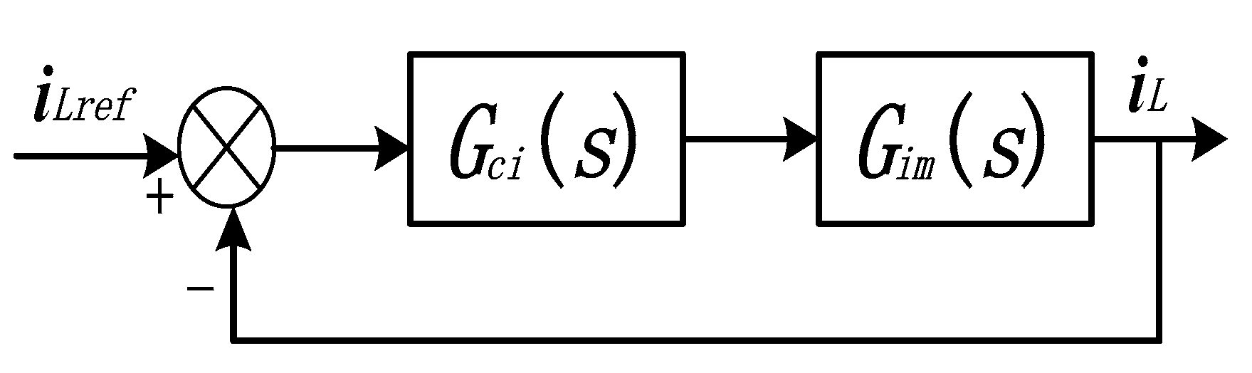
3.2. Current Inner Loop Control

The control block diagram of the current inner loop is shown in Figure 7. Gim(s) is the transfer function of current power level, and Gci(s) is the PI control.
The transfer function of PI control can be expressed as Equation (26).
G c i ( s ) = K p i × 1 + T i c s T i c s = K p i + K i i s
where Kpi is the gain of current controller, which can be obtained by Equation (27). Kii is the current loop integration coefficient and Tic is the current loop integration time constant, which can be obtained by Equation (28). fc is the shear frequency, so the phase margin of the current loop near the shear frequency should be large enough. fd is the compensation zero of the current loop controller.
k p i = 2 π f c L V o k s i
T i c = 1 2 π f d
Since the switching frequency of the system is 60 kHZ, the crossing frequency of the current loop was set as 1/10 of the switching frequency, which was 6 kHz. Figure 8a is the open-loop Bode diagram of the inner current loop before compensation, and Figure 8b is the open-loop Bode diagram of the inner current loop after compensation. The phase margin was about 60°, which met the requirement of system stability. The crossing frequency was 6 kHz, which is consistent with the design value.

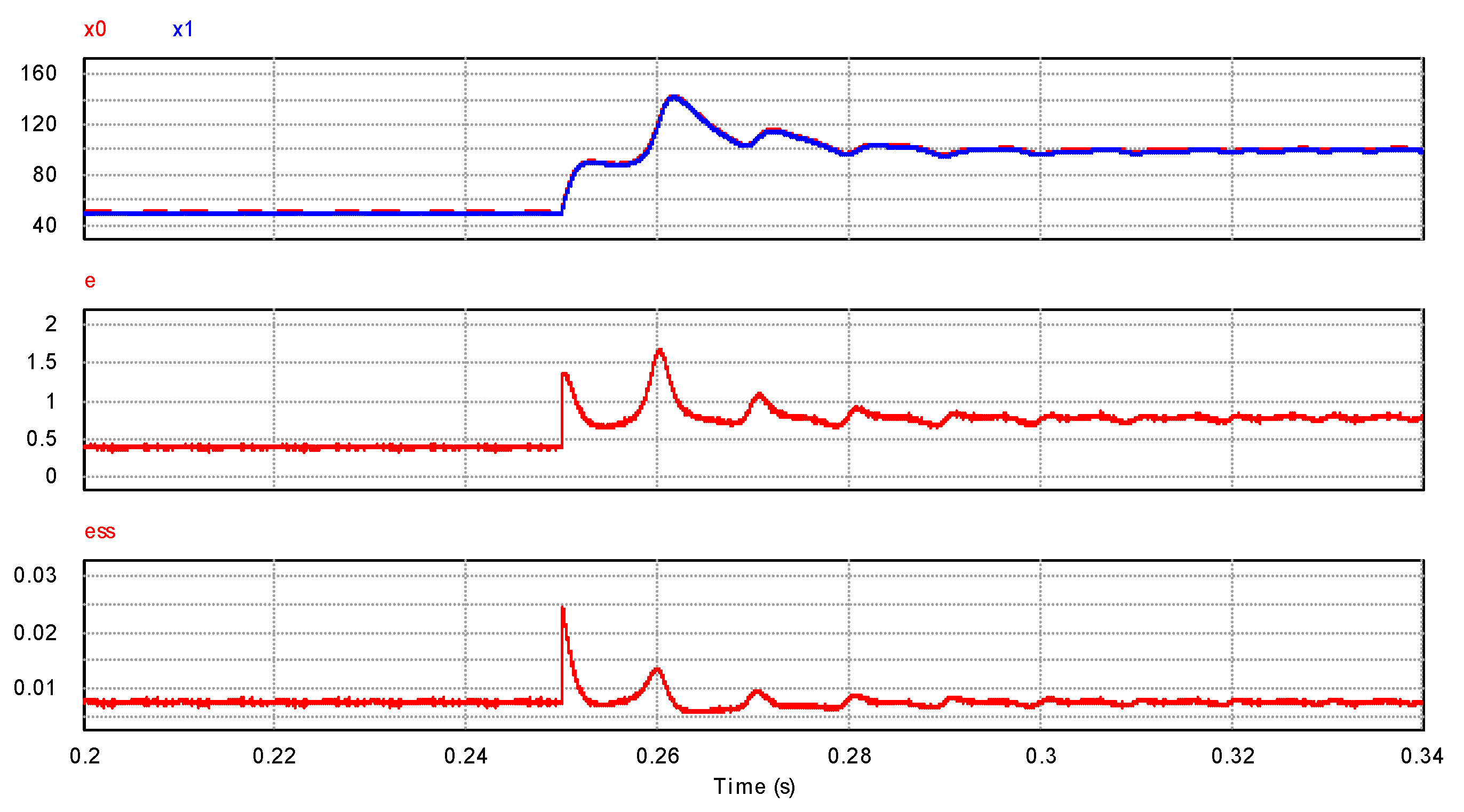
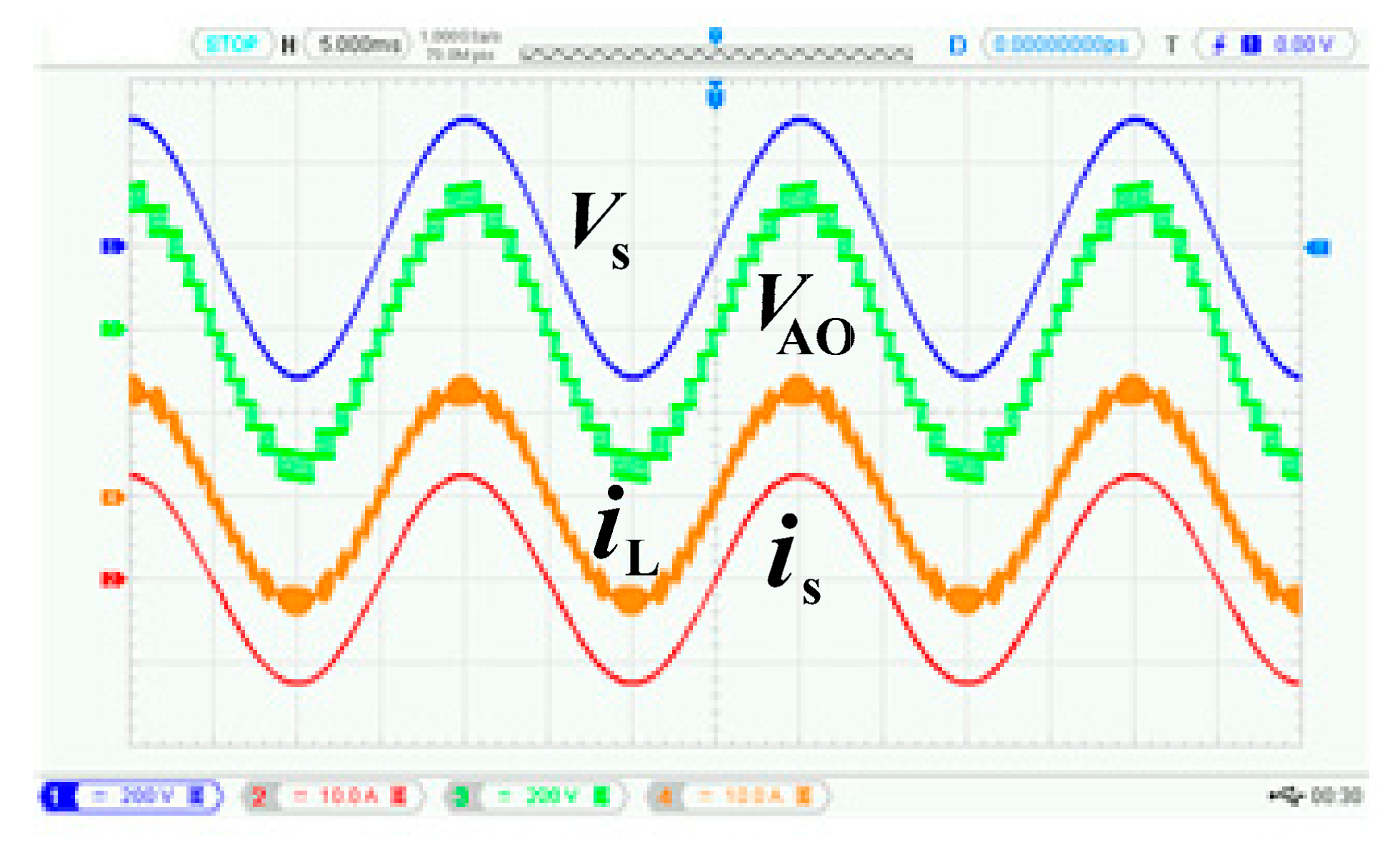
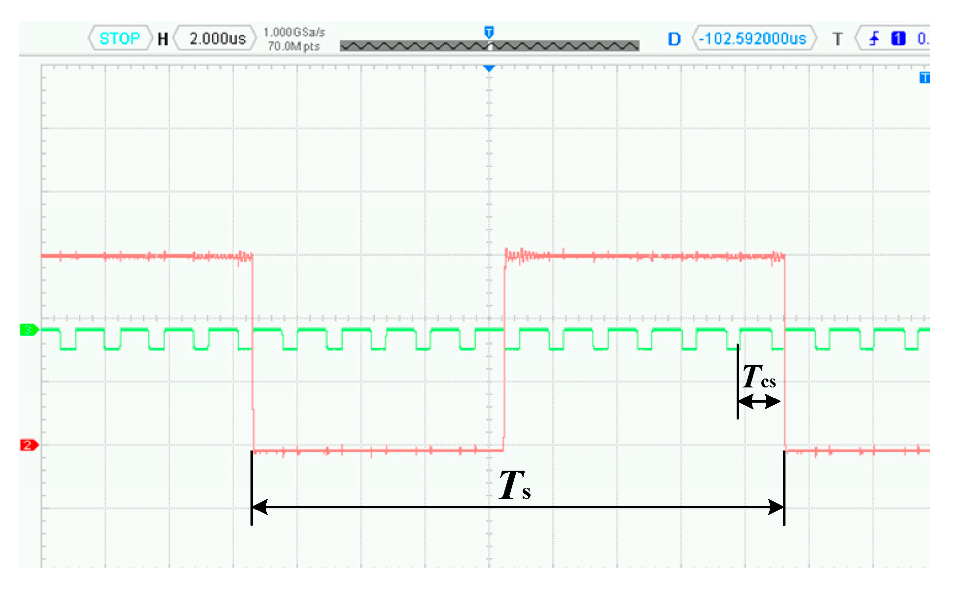
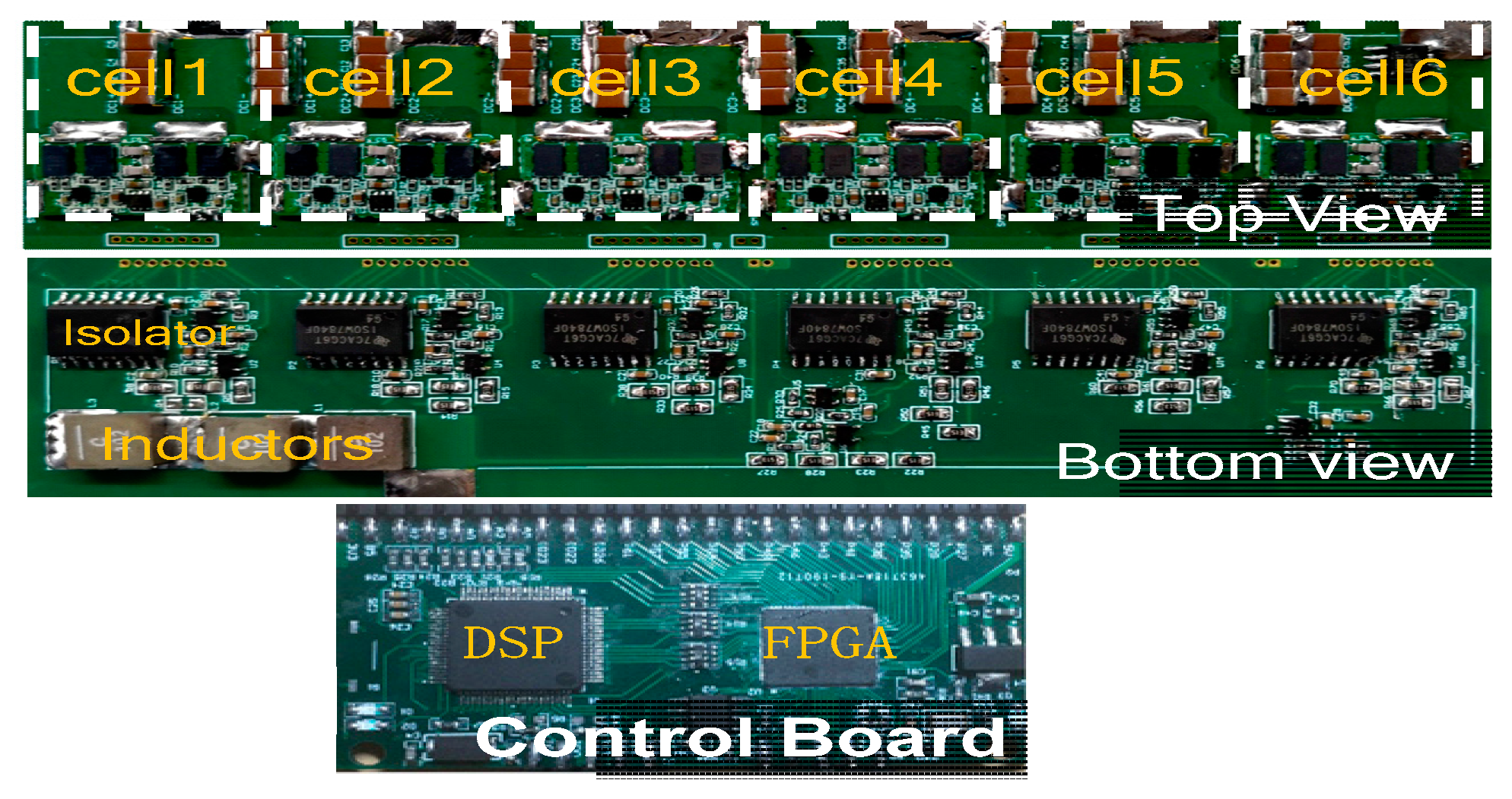
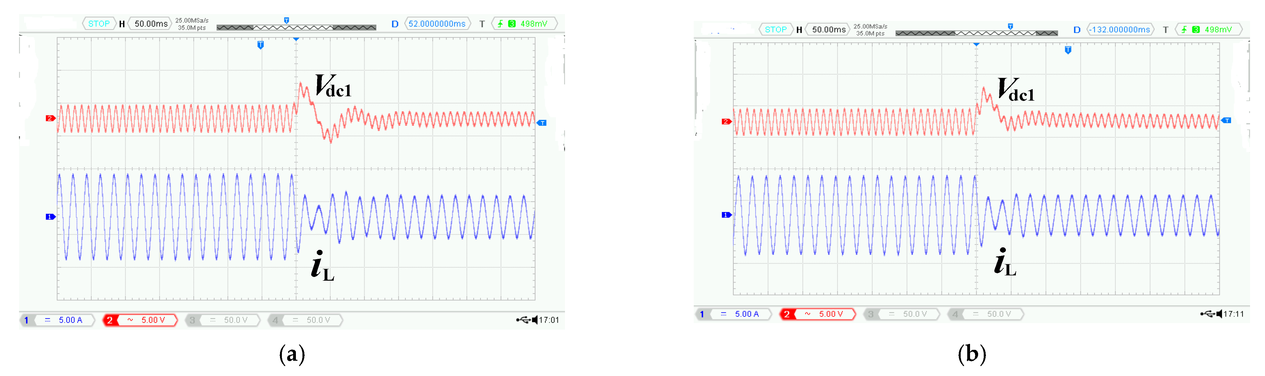
4. System Experimental Analysis

The experiment adopted a PFC prototype with a rated power of 2 kW, the main circuit adopted a CHB topology of six units, the switch adopted a 100 V 4 mΩ gallium nitride device, and the control chip was composed of DSP and FPGA. The picture of the main circuit and control circuit of the experimental prototype is shown in Figure 9. Important components and models used in the prototype are shown in Table 1. Experimental parameters used in the prototype are shown in Table 2.

4.1. System Steady-State Experimental Analysis

Figure 10 is the system steady-state experimental waveform where vs. is the power supply voltage at the AC side of the system; VAO is the bus voltage at the AC side of the system; and is is the bus current at the AC side of the system and iL is the current of boost inductor L. Figure 11 is the system switching cycle waveform. Ts is the normal switching cycle of each switch, and Tcs is the switching period of each switch after carrier phase-shifting modulation.
In order to minimize the volt second of the inductance, it is necessary to ensure that the difference between the voltage at two points of AO and the input voltage is not greater than one level voltage during modulation. With the increase in the number of levels, the inductance volume gradually decreases. It is obvious from Figure 10 that when the input voltage is 220 V, all 13 level voltages will appear between AO, so the voltage borne by each switch tube is greatly reduced. Under full load conditions, the phase difference between the grid current and voltage is very small, and PF can reach 0.99. For the switching cycle, it can be clearly found from Figure 11 that the switching frequency of each switch tube is 60 kHZ. Through carrier phase-shifting control, the equivalent frequency is increased by 12 times to 720 kHZ, which greatly reduces the burden of each switch tube and reduces the switching loss.

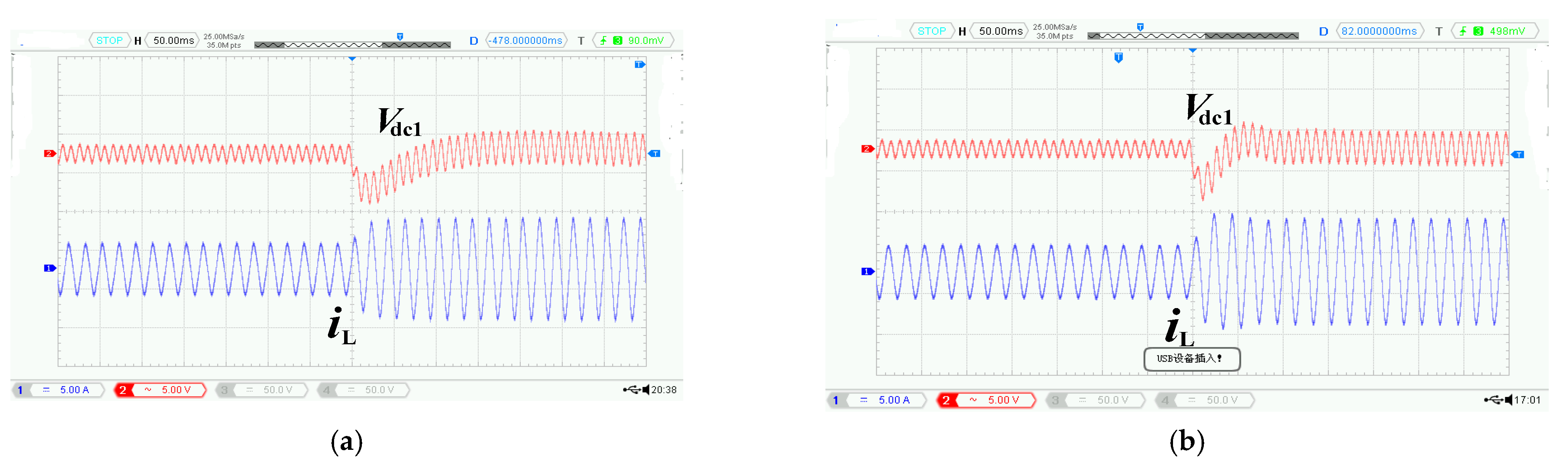
4.2. System Dynamic Experimental Analysis

Figure 12 is the experimental waveform. Vdc1 is the voltage of the output capacitor C1, and iL is the current of boost inductor L. It shows the load from 144 Ω changed to 72 Ω. The response of output voltage and input current was obtained. After the system was put into operation, when the load changed abruptly from 144 Ω to 72 Ω, it can be seen from Figure 12a that under the conventional PI double loop control, the output voltage overshoot was large, and reached a new stable state after about 0.15 s adjustment; after 0.05 s adjustment, the output current reached a new stable state. It can be seen from Figure 12b that under predictive PI control, the output voltage overshoot was relatively small and reached a new stable state after about 0.075 s adjustment; the output current reached a new stable state after 0.05 s of adjustment. Through the previous comparison, it can be seen that the system adopted predictive PI control; in the case of load mutation, the overshoot was small, and the dynamic performance was significantly improved.
Figure 13 is the experimental waveform. Vdc1 is the voltage of the output capacitor C1, and iL is the current of boost inductor L. It shows the load from 72 Ω changed to 144 Ω. The response of output voltage and input current was obtained. After the system was put into operation, when the load changed abruptly from 72 Ω to 144 Ω, it can be seen from Figure 13a that under the conventional PI double loop control, the output voltage overshoot was large, and it reached a new stable state after about 0.15 s of adjustment; After 0.1 s adjustment, the output current reached a new stable state. It can be seen from Figure 13b that under predictive PI control, the output voltage overshoot was relatively small and reached a new stable state after about 0.075 s of adjustment; the output current reached a new stable state after 0.05 s of adjustment. Through the previous comparison, it can be seen that the system adopted predictive PI control; in the case of load mutation, the overshoot was small, and the dynamic performance was significantly improved.

5. Conclusions

In this paper, according to the characteristics of the double frequency fluctuation of input power of the single-phase AC-DC power converter and the non-minimum phase characteristics of the circuit, a single-phase cascade structure control method based on CHB PFC was proposed. The cascaded multilevel main circuit of the system was modeled by small signal, and the double loop control system of current inner loop and voltage outer loop was established. The results were verified by the experiments, and conclusions were drawn as follows.
(1)
The cascaded multilevel structure can effectively improve the system power density of the charger, reduce the voltage drop borne by a single switch, and improve the power factor of the system output.
(2)
The carrier phase shift control strategy was adopted to greatly increase the system switching frequency to reduce the burden of each switch and reduce the switching loss.
(3)
Predictive PI control was adopted in the voltage loop to effectively improve the dynamic stability of the system.

Author Contributions

G.S. conceived the topology and performed the simulations and experiments; Y.Q. conducted the experiment and analyzed the data. All authors have read and agreed to the published version of the manuscript.

Funding

This research was funded by the Key Research Project of Anhui Education Department (Nos. KJ2021A1139 and KJ2019A0860).

Conflicts of Interest

The authors declare no conflict of interest.

References

  1. IEA. Global-ev-Outlook-2018. Available online: https://webstore.iea.org/global-ev-outlook-2018 (accessed on 2 February 2022).
  2. Bortis, D.; Neumayr, D.; Kolar, J.W. ηρ-Pareto optimization and comparative evaluation of inverter concepts considered for the GOOGLE Little Box Challenge. In Proceedings of the 2016 IEEE 17th Workshop on Control and Modeling for Power Electronics (COMPEL), Trondheim, Norway, 27–30 June 2016; pp. 1–5. [Google Scholar]
  3. Chou, D.; Fernandez, K.; Pilawa-Podgurski, R.C.N. An Interleaved 6-Level GaN Bidirectional Converter for Level II Electric Vehicle Charging. In Proceedings of the 2019 IEEE Applied Power Electronics Conference and Exposition (APEC), Phoenix, AZ, USA, 14–17 June 2021; pp. 594–600. [Google Scholar]
  4. Liu, Z.; Li, B.; Lee, F.C.; Li, Q. High-Efficiency High-Density Critical Mode Rectifier/Inverter for WBG-Device-Based on-Board Charger. IEEE Trans. Ind. Electron. 2017, 64, 9114–9123. [Google Scholar] [CrossRef]
  5. Maheswaria, K.T.; Bharanikumara, R.; Arjunb, V.; Amrishb, R.; Bhuvanesh, M. A comprehensive review on cascaded H-bridge multilevel inverter for medium voltage high power applications. Mater. Today Proc. 2021, 45, 2666–2670. [Google Scholar] [CrossRef]
  6. Hurley, W.G.; Wölfle, W.H. Transformers and Inductors for Power Electronics: Theory, Design and Applications; John Wiley & Sons: Hoboken, NJ, USA, 2013. [Google Scholar]
  7. Babu, J.J.; Thirumavalavan, V. Variable Duty Cycle Control with PSO-PI Controller for Power Factor Correction and Fast Regulation. J. Inst. Eng. India Ser. B 2021, 1–9. [Google Scholar] [CrossRef]
  8. Cai, Y.; Xu, J.; Yang, P.; Liu, G. Design of double-line-frequency ripple controller for quasi-single-stage AC/DC converter with audio susceptibility model. IEEE Trans. Ind. Electron. 2019, 66, 9226–9237. [Google Scholar] [CrossRef]
  9. Villarroel, F.A.; Espinoza, J.R.; Pérez, M.A.; Ramírez, R.O.; Baier, C.R.; Sbárbaro, D.; Silva, J.J.; Reyes, M.A. Stable Shortest Horizon FCS-MPC Output Voltage Control in Non-Minimum Phase Boost-Type Converters Based on Input-State Linearization. IEEE Trans. Energy Convers. 2021, 36, 1378–1391. [Google Scholar] [CrossRef]
  10. Su, Y.; Ge, X.; Xie, D.; Wang, K. An Active Disturbance Rejection Control-Based Voltage Control Strategy of Single-Phase Cascaded H-Bridge Rectifiers. IEEE Trans. Ind. Appl. 2020, 56, 5182–5193. [Google Scholar] [CrossRef]
  11. Ming, W.L.; Zhong, Q.C.; Zhang, X. A Single-Phase Four-Switch Rectifier With Significantly Reduced Capacitance. IEEE Trans. Power Electron. 2015, 31, 1618–1632. [Google Scholar] [CrossRef] [Green Version]
  12. Bai, L.; Ren, X.; Hui, Q.; Wu, Y.; Li, K.; Guo, Z.; Zhang, Y. Dynamic response optimization forinterleaved boost PFC converter with improved dual feedforward control. In Proceedings of the 2017 IEEE Energy Conversion Congress & Exposition, Cincinnati, OH, USA, 1–5 October 2017; pp. 5280–5286. [Google Scholar]
  13. Leung, K.H.; Loo, K.H.; Lai, Y.M. A Family of Ripple Estimation-Cancellation Methods Based on Switched-Resistor Circuits and Their Application in Fast-Response PFC Preregulator. IEEE Trans. Power Electron. 2017, 32, 2608–2621. [Google Scholar] [CrossRef]
  14. Yao, C.; Zhang, Y.; Chen, H. Adaptive Constant Power Control of MHz GaN-Based AC/DC Converters for Low Power Applications. IEEE Trans. Ind. Appl. 2018, 54, 2525–2533. [Google Scholar] [CrossRef]
  15. Mallik, A.; Lu, J.; Khaligh, A. Sliding Mode Control of Single-Phase Interleaved Totem-Pole PFC for Electric Vehicle Onboard Chargers. IEEE Trans. Veh. Technol. 2018, 67, 8100–8109. [Google Scholar] [CrossRef]
  16. Li, S.; Lu, W.; Yan, S.; Zhao, Z. Improving Dynamic Performance of Boost PFC Converter Using Current-Harmonic Feed forward Compensation in Synchronous Reference Frame. IEEE Trans. Ind. Electron. 2020, 67, 4857–4866. [Google Scholar] [CrossRef]
  17. Xiao, D.; Alam, K.S.; Norambuena, M.; Rahman, M.F.; Rodriguez, J. Modified Modulated Model Predictive Control Strategy for a Grid-Connected Converter. IEEE Trans. Ind. Electron. 2021, 68, 575–585. [Google Scholar] [CrossRef]
  18. Kwak, S. Model predictive direct power control with vector preselection technique for highly efficient active rectifiers. IEEE Trans. Ind. Inform. 2015, 11, 44–52. [Google Scholar] [CrossRef]
  19. He, T.; Lu, D.D.-C.; Li, L.; Zhang, J.; Zheng, L.; Zhu, J. Model-Predictive Sliding-Mode Control Three-Phase AC/DC Converters. IEEE Trans. Power Electron. 2018, 33, 8982–8993. [Google Scholar] [CrossRef]
  20. Vazquez, S.; Rodriguez, J.; Rivera, M.; Franquelo, L.G.; Norambuena, M. Model predictive control for power converters and drives: Advances and trends. IEEE Trans. Ind. Electron. 2017, 64, 935–947. [Google Scholar] [CrossRef] [Green Version]
  21. Qi, C.; Chen, X.; Tu, P.; Wang, P. Cell-by-Cell-Based Finite-Control-Set Model Predictive Control for a Single-Phase Cascaded H-Bridge Rectifier. IEEE Trans. Power Electron. 2018, 33, 4857–4866. [Google Scholar] [CrossRef]
  22. Leung, K.H.; Loo, K.H.; Lai, Y.M. Unity-power-factor control based on precise ripple cancellation for fast-response PFC preregulator. IEEE Trans. Power Electron. 2016, 31, 3324–3337. [Google Scholar] [CrossRef]
  23. Zheng, D.; Ren, Z.Y.; Fang, J.A. Stability analysis of multiple time-delayed system. ISA Trans. 2008, 47, 439–447. [Google Scholar] [CrossRef]
  24. Airikka, P. Stability analysis of a predictive PI controller. In Proceedings of the 2013 21st Mediterranean Conference on Control and Automation, Platanias, Greece, 25–28 June 2013; pp. 1380–1385. [Google Scholar]
Figure 1. Topology of a single-phase N-cell CHB PFC.
Wevj 13 00048 g001
Figure 2. Modulation waveforms of unit i and unit i + 1.
Wevj 13 00048 g002
Figure 3. Control schematic diagram of the PFC system.
Wevj 13 00048 g003
Figure 4. Schematic diagram of predictive PI control.
Wevj 13 00048 g004
Figure 5. The open-loop Bode diagram of the outer voltage loop: (a) Open loop Bode diagram of voltage loop before compensation and (b) open loop Bode diagram of compensated voltage loop.
Wevj 13 00048 g005
Figure 6. Error and absolute error between the actual value and predicted value of PI control.
Wevj 13 00048 g006
Figure 7. Control schematic diagram of the PFC system’s current inner loop.
Wevj 13 00048 g007
Figure 8. The open-loop Bode diagram of the inner current loop: (a) Open loop Bode diagram of current loop before compensation; (b) Open loop Bode diagram of compensated current loop.
Wevj 13 00048 g008
Figure 9. Photo of the main circuit and control circuit of the experimental prototype.
Wevj 13 00048 g009
Figure 10. AC side experimental waveform of the steady-state system.
Wevj 13 00048 g010
Figure 11. Switching cycle waveform.
Wevj 13 00048 g011
Figure 12. Output voltage and input current response to load change from 144 Ω to 72 Ω: (a) Traditional double loop PI control; (b) predictive PI control.
Wevj 13 00048 g012
Figure 13. Output voltage and input current response to load change from 72 Ω to 144 Ω: (a) Traditional double loop PI control; (b) predictive PI control.
Wevj 13 00048 g013
Table 1. Important components and models used in the prototype.
ComponentModel
Switch tubeEPC2032
IsolatorISOW7840
DriverLMG1205
Driver power supplyTPS60150
Current sensorACS723
DSPTMS320F28069
FPGAAL3S10NG88
Table 2. Experimental parameters used in the prototype.
ParameterValues
Main inductance5 μH
Filter inductance8 μH
Filter capacitor620 nF
Unit bus capacitance1800 μF
Unit resistive load12 Ω
Switching frequency60 kHz
AC side phase voltage220 V
DC side voltage360 V
Rated power2 kW
Power density1500 W/in3
Publisher’s Note: MDPI stays neutral with regard to jurisdictional claims in published maps and institutional affiliations.

