Article

A Mayfly-Based Approach for CMOS Inverter Design with Symmetrical Switching

Electrical Engineering Department, Faculty of Engineering, Jordan University of Science and Technology, Irbid 22110, Jordan
*
Author to whom correspondence should be addressed.
Algorithms 2023, 16(5), 237; https://doi.org/10.3390/a16050237
Submission received: 29 March 2023 / Revised: 23 April 2023 / Accepted: 25 April 2023 / Published: 30 April 2023

Abstract

:
This paper presents a novel approach to designing a CMOS inverter using the Mayfly Optimization Algorithm (MA). The MA is utilized in this paper to obtain symmetrical switching of the inverter, which is crucial in many digital electronic circuits. The MA method is found to have a fast convergence rate compared to other optimization methods, such as the Symbiotic Organisms Search (SOS), Particle Swarm Optimization (PSO), and Differential Evolution (DE). A total of eight different sets of design parameters and criteria were analyzed in Case I, and the results confirmed compatibility between the MA and Spice techniques. The maximum discrepancy in fall time across all design sets was found to be 2.075711 ns. In Case II, the objective was to create a symmetrical inverter with identical fall and rise times. The difference in fall and rise times was minimized based on Spice simulations, with the maximum difference measuring 0.9784731 ns. In Case III, the CMOS inverter was designed to achieve symmetrical fall and rise times as well as propagation delays. The Spice simulation results demonstrated that symmetry had been successfully achieved, with the minimum difference measuring 0.312893 ns and the maximum difference measuring 1.076540 ns. These Spice simulation results are consistent with the MA results. The results conclude that the MA is a reliable and simple optimization technique and can be used in similar electronic topologies.

1. Introduction

The inverter is known as the basic logic gate of any digital Integrated Circuit (IC) technology, and it is an integral part of all digital systems. With the emergence of new technologies, designers are focusing on building the basic blocks, such as inverters [1,2]. Much work has been conducted to overcome the performance bottleneck in CMOS inverters [3]. The inverters’ performance has been investigated in order to come up with robust circuits [4]. As technology has been sized down, circuit design has become more challenging, and the need for designing accurate and fast circuits with low time delay has become an important issue [5,6]. The switching characteristics of the inverter are the fundamental parameters used to describe the inverter’s performance. Thus, the switching speed of the inverter’s circuit should be optimized before the design steps to achieve symmetrical switching. Switching time from high to low or from low to high depends on the channel width, length of the transistors, and load capacitance CL.
The physical structure of the transistors in the CMOS inverter causes parasitic capacitances, because of the segregation of mobile charges across different regions within the device. The value of parasitic capacitances in a transistor depends on its width (W) and the length (L) of its channel. The currents charging and discharging these capacitances are ICh and IDis, respectively. ICh is responsible for the rise time and IDis is responsible for the fall time. The flow of ICh is through the pull-up section and the flow of IDis flow is through the pull-down section [7]. The significance of output rise and fall time has been discussed on numerous occasions [8,9,10,11,12]. To ensure symmetrical sequence many techniques have been developed. In Ref. [7] two additional transistors were added to regulate the same amount of current from Vdd to match ICh with IDis. The problem with this method is that the addition of new transistors will lead to larger size circuits and can introduce more noise to the circuit. Others have used time-delay elements to correct the mismatch in the time delay on a chip [13,14]. Nevertheless, creating delay elements can be a challenging task due to their extensive design specifications and various trade-offs involved. In this work, instead of adding any new transistors, we focus on matching the rise time and the fall time by finding the optimum values of W and L using the Mayfly Algorithm.
Optimization algorithms use mathematical techniques to iteratively refine the solution until the optimal value is achieved. There are various optimization algorithms available in the literature. Gradient descent [15,16], genetic algorithms [17,18,19], RMSProp [20], and many other optimization algorithms have been used to improve the efficiency and accuracy of solving complex problems. In the published literature, different evolutionary optimization methods have been used to design inverters with optimal switching characteristics. For instance, the PSO technique was used to design the CMOS inverter and its transient performance [21,22]. The authors investigated the overall performance of the PSO technique. In [23,24], the PSO algorithm was used to design a nano-scale CMOS inverter to improve its symmetrical switching. The results of the PSO method were compared to Spice simulation results.
In [25,26,27,28,29], De, Bishnu Prasad, et al., implemented different optimization techniques to obtain the symmetrical switching characteristic of CMOS inverters. In [25], the PSO with constriction factor and inertia weight approach PSO-CFIWA was used to get the optimal symmetrical switching properties of the CMOS inverter. The performance of the PSO-CFIWA method was compared to that of the real coded genetic algorithm (RGA) and the results showed an improved performance of the PSO-CFIWA. Two different evolutionary optimization methods (DE and RGA) were used in [26] to obtain an optimal global design. The DE and RGA methods were applied to three different studies with different design parameter ranges and the comparison between them was presented. The DE method was found to be the least cost-effective function compared to other design methods. The Craziness-based Particle Swarm Optimization (CRPSO), presented in [27], was used to design the CMOS inverter with the optimal switching speed characteristics. The results of the CRPSO method were compared to the RGA method results and the CRPSO method gave better symmetrical switching for the CMOS inverter. In [28], a hybrid meta-heuristic search method was suggested with a harmony search algorithm (HS) and DE algorithm. This method was called HS-–DE and it was used in CMOS inverter design with symmetrical switching properties to find an improved global solution. The results of HS–DE were compared with PSPICE results. In [29], the PSO with an aging leader and challenger (ALCPSO) method was employed to design the CMOS inverter with the optimal symmetrical switching characteristics. The simulation results of the ALCPSO method were compared with the simulation results of the RGA. In [30], a Cuckoo Search Algorithm (CSA), inspired by the parasitic nature brood of a few cuckoo types, was used to optimize the CMOS inverter and to achieve equal values of both the fall time (tf) and rise time (tr). The CSA algorithm was also used to achieve equal propagation delay time when switching from low to high and from high to low. The results of the CSA were compared with different methods such as the PSO, the RGA, and the PSO-CFIWA methods. The authors in [31] used different optimization methods to derive the accuracy equation for the propagation delay time of a ring oscillator. In [32], the SOS was presented to determine the best values of the channel width (W), length (L), and the output-load’s capacitance (CL) to achieve symmetrical switching characteristics for the CMOS inverter. The modified approach for Multi-Objective Optimization of Heat Transfer Search (MOMHTS) was presented in [33]. The MOMHTS method was applied to five problem sets. The modified optimizer method was compared to Multi-Objective Symbiotic Organism Search (MOSOS), Multi-Objective Synchronous Heat Transfer (MOHTS), Multi-Objective Ant System (MOAS), and Multi-Objective Ant Colony System (MOACS).
A novel MA was presented in [34]. The MA is an optimization algorithm used to find the best solution to a problem in terms of the convergence position and convergence speed. The authors in [34] compared the results of the MA with the PSO and Firefly Algorithm (FA) algorithms. The MA was improved in [35]. The equations of the velocity were updated to achieve better results. In [36], the authors conducted research to examine the key role of the oppositional mayfly optimization for the use in tasks scheduling technique (OMO-TST) related to the cloud computing environment (CC). The OMO–TST was implemented, and the cloud computing environment performance was optimized and controlled. The results showed that implementing the OMO–TST technique for CC can contribute to a significant reduction in the level of complexity related to the computations required for processing data in a cloud system. In addition, the results of their analysis revealed that utilizing the OMO technique for CC can achieve practical usage of resources and enhance the performance of CC at the level of individuals and companies. In [37], the performance of the negative mayfly optimization method is presented to get the best positions and velocities of the mayflies.
The MA was utilized by researchers to solve various problems and obtain optimal solutions. In a study conducted by Bhattacharyya, et al., the role of MA in machine learning was evaluated for reducing the dataset dimension by eliminating redundant and excessive characteristics [38]. A novel feature collection method, MA–HS, was developed to achieve this goal [38]. The MA–HS was employed to enhance feature selection performance by improving the search space and fitness function. The experimental results showed that it outperformed other algorithms such as the genetic algorithm (GA), binary dragonfly algorithm (BDA), binary salp swarm algorithm (BSSA), and whale optimization algorithm (WOA) [38]. Work was conducted to employ the initial center frequency-guided filter (ICFGF) approach to detect bearing faults through a two-phase process [39]. In the first phase, energy spectrum distributions were assessed using a variation analysis scale. In the second phase, a modified Mayfly optimization method (MMA) was used to determine the optimal resonance demodulation frequency. Employing the MMA in the ICFGF was found to be effective in detecting faults with high accuracy, as evidenced by results from [39]. The study also compared ICFGF to other techniques such as conditional variation selection and fast kurtogram, demonstrating its superior performance. The Mayfly method was also used to optimize the model of combined cooling heat and power (CCHP) systems [40]. The authors in [40] were able to obtain the optimal size of the components and minimum fuel consumption in the system. It was noted that the Mayfly Algorithm was more effective in providing the required solution in a shorter time. Researchers carried out a study assessing the major contribution of implementing the MA to conduct optimization of the performance of solar photovoltaic thermal collectors PVTC that are integrated with an electric hydrogen generation system [41]. To achieve the study goal, a solar (PVTC) with a hydrogen generation system has been modeled for predicting several factors related to the performance of the system using artificial intelligence and the Mayfly Algorithm. The MA has been used to improve the forecasting accuracy in the model.
The aim of this research is to utilize the Mayfly Algorithm to determine the ideal circuit parameters that result in minimal rise time in Case I. In Case II, the goal is to use the same algorithm to find the optimal circuit parameters that produce symmetrical fall and rise times for the inverter. In Case III, the focus will be on finding the optimal circuit parameters that lead to an output waveform with symmetrical rise and fall times, as well as a symmetrical propagation delay time. The rest of this paper is organized as follows: the MA is briefly described in Section 2; the switching characteristics of the CMOS inverter are presented in Section 3; Section 4 explains the formulation of the problem; results and Spice simulations are provided in Section 5; finally, Section 6 concludes the paper.

2. Mayfly Optimization Algorithm

Optimization problem-solving techniques can be classified into two categories. The first category is heuristic methods, such as kinetic gas molecules, evolutionary programming, particle swarm optimization, simulated annealing, genetic algorithm, and Mayfly Algorithm [38]. The second category is mathematical methods, such as linear programming, nonlinear programming, and mixed-integer linear programming [42].
The main goal of an optimization algorithm is to determine the optimal solution to an optimization problem. The MA is a recently proposed algorithm by Zervoudakis and Tsafarakis in 2020 [34]. The MA is based on the mayfly’s mating procedure and the flight behavior that combines the evolutionary algorithms and the best features of the swarm intelligence optimization algorithms [34]. In MA, two population sets are randomly generated to represent the female and male sets of the mayflies. The position of each mayfly in the problem space represents a candidate solution to the optimization problem. The mayfly’s position is given by an n-dimensional vector x = (x1, x2, …, xn), where the objective function is computed to evaluate each mayfly’s performance. Each mayfly’s position is updated using its velocity, given by the vector v = (v1, v2, …, vn), and flying direction. The mayfly’s flying direction is determined by the best individual flying experiences of each mayfly’s pbest and the best swarm’s social flying experiences gbest [34].
The individuals in the MA update their location in the problem space based on their current positions pit and their velocity vit for each iteration using Equation (1) [34].
P i t + 1 = P i t + V i t + 1
In the Mayfly Algorithm, a mayfly’s velocity can be explained as the alteration in its location. The flight path of a mayfly is influenced by a complex interplay of its own and the group’s flying encounters. Every mayfly modifies its flight path to get closer to its optimal position (“pbest”) and the most favorable position acquired by any mayfly in the swarm (“gbest”).
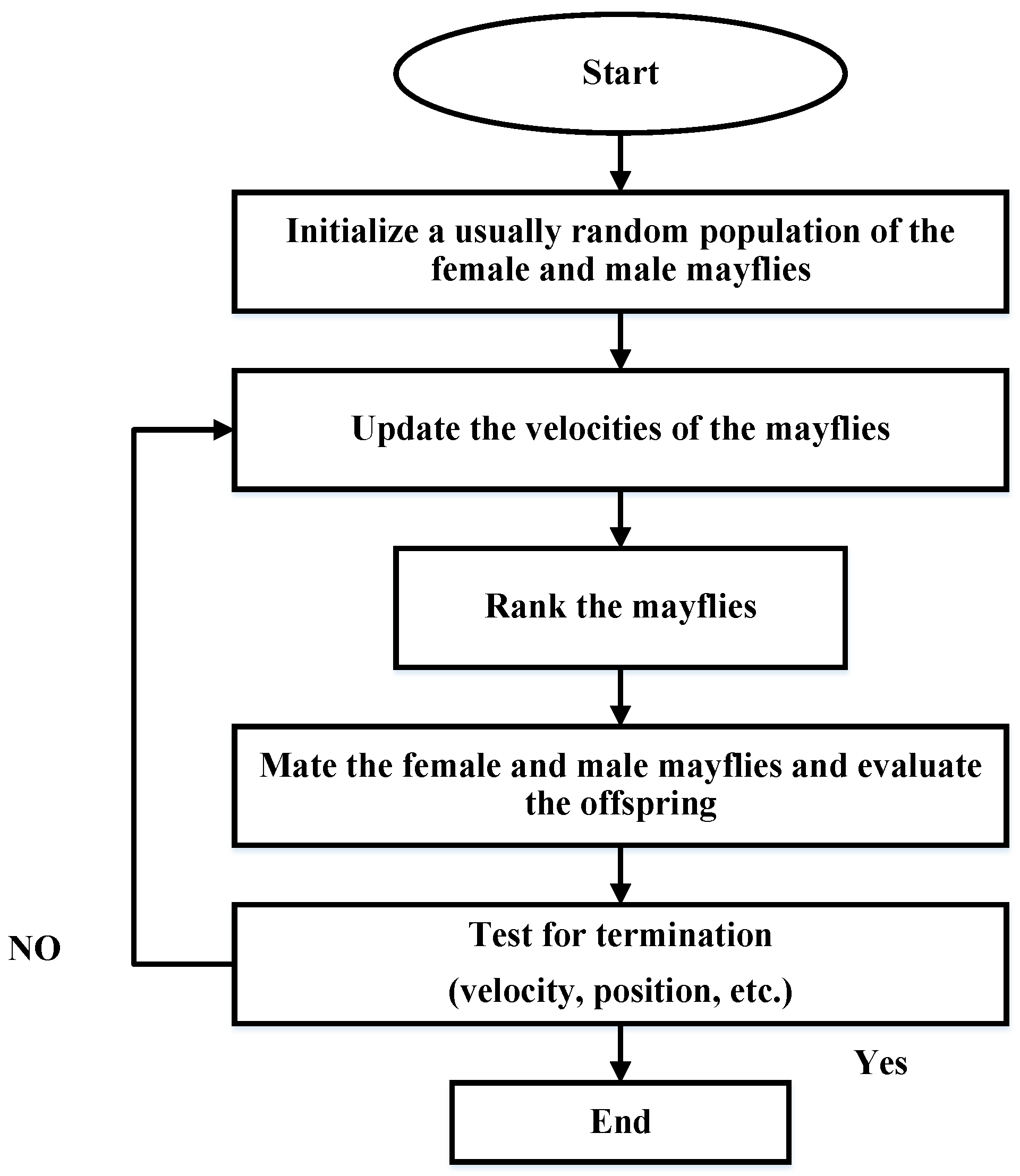
The working mechanism of the MA is presented in the following discussion.

2.1. Movement of Male Mayflies

In each iteration, the male mayflies continue the exploring process in swarms. The position of a male mayfly is updated using Equation (2) [34].
x i t + 1 = x i t + v i t + 1
where xit is the current position of the male mayfly at time step t, and vit+1 is the mayfly’s velocity. The male mayflies fly a few meters above the water’s surface and evolve at high speeds. The velocity of a male mayfly is calculated as in Equation (3) [34].
v i j t + 1 = v i j t + a 1 e β r p 2 p b e s t i j x i j t + a 2 e β r g 2 g b e s t i j x i j t
where a1 and a2 are the personal and global positive coefficients, respectively, rp and rg are the Cartesian distance for personal and global positions, respectively, β represents visibility coefficient, pbest is the best position of a mayfly and gbest is the best global position of a mayfly.
The velocity of the best male mayflies in the current iteration is updated using Equation (4) [34].
V i j t + 1 = v i j t + d × r
where d is the nuptial dance parameter and r is a random number in the range [−1, 1].

2.2. Movement of Female Mayflies

The female mayflies’ velocity depends on the distance between the females and the males. The female mayflies fly to the male mayflies for mating. The position of a female Mayfly is updated using Equation (5) [34].
Yit+1 = yit + vit+1
where yit is the current position of the female mayfly at time step t. In the MA, the best female. The velocity of the female is calculated using Equation (6) [34].
v i j t + 1 = v i j t + a 2 e β r m f 2 x i j t y i j t           if   f y i f ( x i ) v i j t + fl * r           if   f y i f ( x i )
where vtij is a female mayfly’s velocity in dimension j at time t, ytij is the position of female mayfly in the dimension j at time t, xtij is the position of male mayfly in j at time t, β and a2 represent visibility coefficient, and a positive constant, respectively, rmf is the Cartesian distance between female and male mayflies, while f1 and r represent a random walk coefficient and a random number in the range [−1, 1], respectively.

2.3. Mating of Mayflies

In MA, each couple of mayflies produces two offspring. One is added to the female population arbitrarily and the other is added to the male population. Two offspring are generated after mating as shown in Equations (7) and (8) [34].
O f f s p r i n g 1 = L × m a l e + ( 1 L ) × f e m a l e
O f f s p r i n g 2 = L × f e m a l e + ( 1 L ) × m a l e
where L is a random number with a Gaussian distribution. The procedure of the MA is described in the flow chart shown in Figure 1 below [36].

3. Switching Characteristics of the CMOS Inverter

The fundamental technology of any digital IC relies on the inverter. The inverter serves as the basic block. Its switching characteristics play a critical role in describing the technology. The performance speed of a digital system is contingent on the switching characteristics of the logic gates. This study employs the MA technique to derive the optimal switching characteristics of CMOS inverters. By analyzing the switching operation of the CMOS inverter, the fall and rise time (tf and tr) and propagation delay times (tPHL and tPLH) are determined [11,12,13,14,15,16,18]. Figure 2 shows the CMOS inverter, while Figure 3 displays the voltage waveforms.
To determine the fall time, one must measure the duration necessary for the output voltage to decrease from 90% to 10% levels. Conversely, the rise time pertains to the time required for the output voltage to increase from 10% to 90% levels. These values can be calculated using Equations (9) and (10), respectively [11,12,13,14,15,16,18].
t f = C L μ n C O X W L n ( V D D V t n ) 2 ( V t n 0.1 V D D ) ( V D D V t n ) + ln 2 V D D V t n 0.1 V D D 0.1 V D D
t r = C L μ p C O X W L p ( V D D V t p ) 2 ( V t p 0.1 V D D ) ( V D D V t p ) + l n ( 2 V D D V t p 0.1 V D D 0.1 V D D )
The duration between the 50% in the rising input voltage and the 50% in the falling output voltage represents the high to low propagation delay. On the other hand, the low to high propagation delay pertains to the time delay between the 50% transition of the falling input voltage and the 50% transition of the rising output voltage. These values can be determined using Equations (11) and (12), respectively [11,12,13,14,15,16,18].
t p H L = C L μ n C O X W L n ( V D D V t n ) 2 V t n ( V D D V t n ) + l n ( 4 V D D V t n V D D 1 )
t p L H = C L μ p C O X W L p ( V D D V t p ) 2 V t p ( V D D V t p ) + l n ( 4 V D D V t p V D D 1 )

4. Problem Formulation

This paper presents three different case studies to obtain the optimal switching characteristics and the optimal performance of the CMOS inverter. In the first one, the fall time tf of the output voltage for the CMOS inverter is evaluated. The second case study aims to design a CMOS inverter with a symmetrical output voltage where values for both rise time’s tr and fall time’s tf are equal. In the third one, the CMOS inverter is designed to achieve a symmetrical output voltage and also to obtain equal propagation delay times (tPHL and tPLH).

4.1. Case I

In this case, the aim is to evaluate the fall time of the output voltage for the CMOS inverter, as previously shown in 9, with the minimum values of the cost function CF. During the design phase, the values of the design parameters—which include the output load capacitance CL, the ratio between channel width and length W/L for both the NMOS and the PMOS structures’ fall-time tf—should be within a specific range. The MA is implemented to find the optimal design parameters CL, W/L, and the tf is needed to minimize the cost function given in Equation (13). The fitness function can be written as in Equation (14) [25,26,27,28,29,30,32].
C F = μ n C O X W L n t f C L ( V D D V t n ) 2 V t n 0.1 V D D V D D V t n + ln 2 V D D V t n 0.1 V D D 0.1 V D D
J = 10 l o g 10 C F
The TSMC 0.25 µm CMOS model in the three case studies. Table 1 shows the eight different design sets which are considered in Case I.

4.2. Case II

To obtain an optimal symmetrical switching response, the fall time must equal the rise time of the output voltage. The main objective, in this case, is to find the inverter design parameters, CL, (W/L)p, and (W/L)n that minimize the cost function given in Equation (15) [25,26,27,28,29,30,32]. This cost function measures the difference between the fall time and rise times of the CMOS inverter.
C F = ( t f ( C L , W L n ) ) ( t r ( C L , W L p ) )
Subject to the following constraints as in Equations (16)–(20) [25,26,27,28,29,30,32].
t f m i n t f t f m a x
t r m i n t r t r m a x
C L m i n C L C L m a x
W L n m i n W L n W L n m a x
W L p m i n W L p W L p m a x
Table 2 shows the eight different design sets considered with the corresponding bound constraints. In this case, the evaluation of the fall time (tf), and the rise time (tr) of the output voltage is implemented for the eight different design sets of the parameters CL, (W/L)p and (W/L)n.

4.3. Case III

In this case, the main objective is to obtain the symmetrical switching characteristics for the CMOS inverter with equal fall time (tf) and rise time (tr), and equal propagation delay times. The cost function that needs to be minimized is formulated as in Equation (21) [25,26,27,28,29,30,32].
C F = ( t f ( C L , W L n ) ) ( t r ( C L , W L p ) ) + ( t p H L ( C L , W L n ) ) ( t p L H ( C L , W L p ) )
Subject to the following constraints as in Equations (16)–(20), (22) and (23) [25,26,27,28,29,30,32].
t p H L m i n t p H L t p H L m a x
t p L H m i n t p L H t p L H m a x
The optimization problem depends on three variables: the load capacitance CL, the ratio between the channel width and length of NMOS and PMOS transistor (W/L)p, and (W/L)n. The eight different design sets are considered with the lower and upper bounds of the constraints and they are shown in Table 3 for Case III.

5. Results

In this section, the optimal switching characteristics of the CMOS inverter are obtained using the Mayfly Optimization Algorithm. A total of eight different design sets are considered with the lower and upper bounds for the design parameters of each design set as seen in Table 1, Table 2 and Table 3 for the three different case studies. TSMC 0.25 µm CMOS model is used in the LT-Spice simulation to get simulation results. The model parameters are VDD = 2.5 V, Vtn = 0.3655 V, Vtp = 0.5466 V, µpCox = 51.6 µA/V2 and µnCox = 243.6 µA/V2 [25,26,27,28,29,30,32].
For Case I, the MA is implemented using MATLAB to find the design parameters needed to minimize the fall time of the output voltage for the CMOS inverter with an identical size of PMOS and NMOS transistors. For each design set in Table 1, the MA parameters are population size (males and females) equal 20 and number of iterations equal 50. The result of the MA gives the optimal design parameters, i.e., CL, (W/L) and (tf), for the CMOS inverter with the minimum fall time. These results are summarized in Table 4. The results show that the design parameters are within the limits given in Table 1.
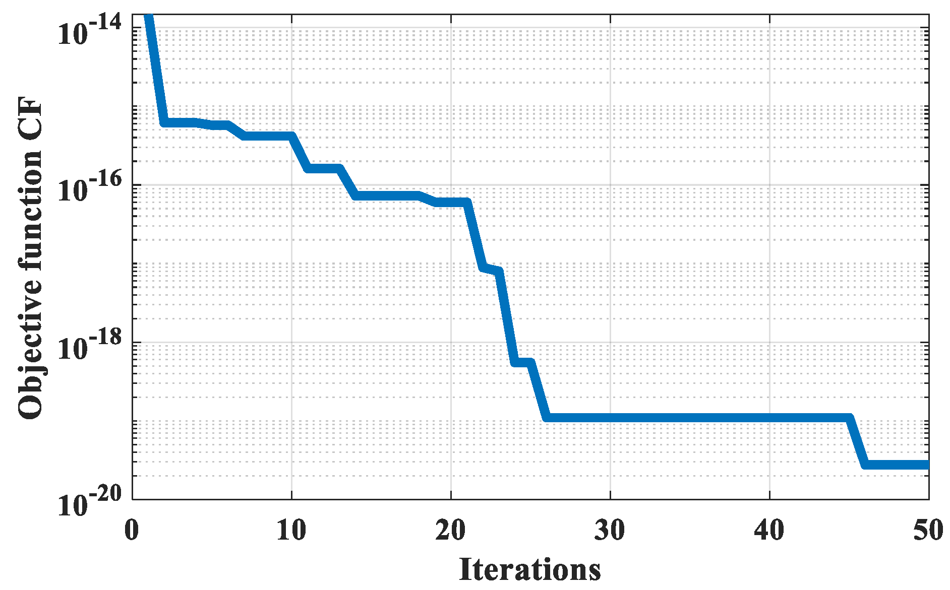
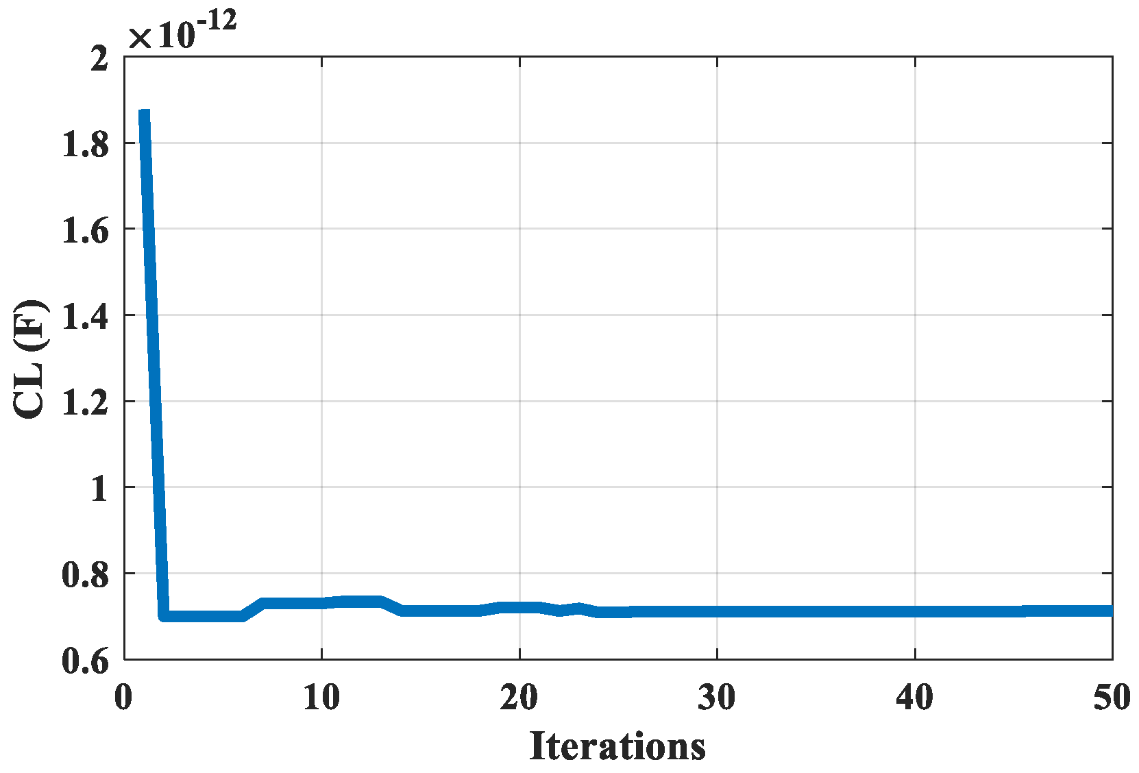
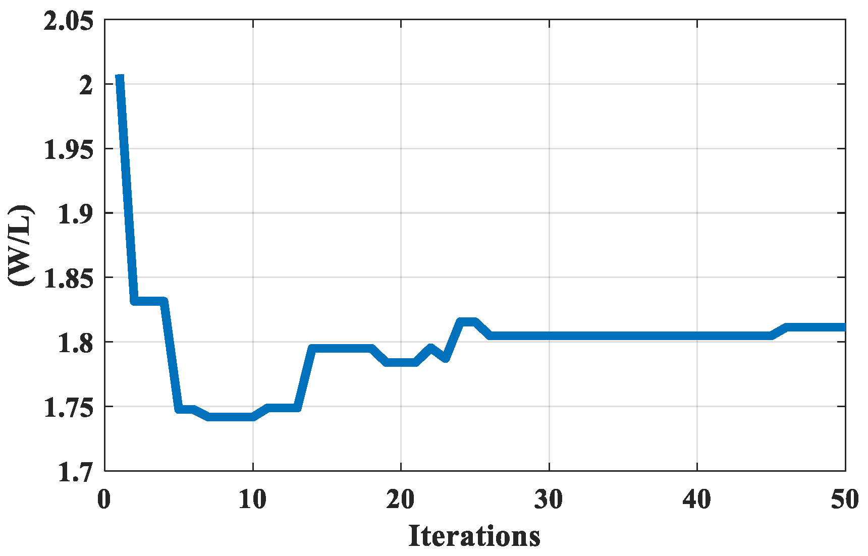
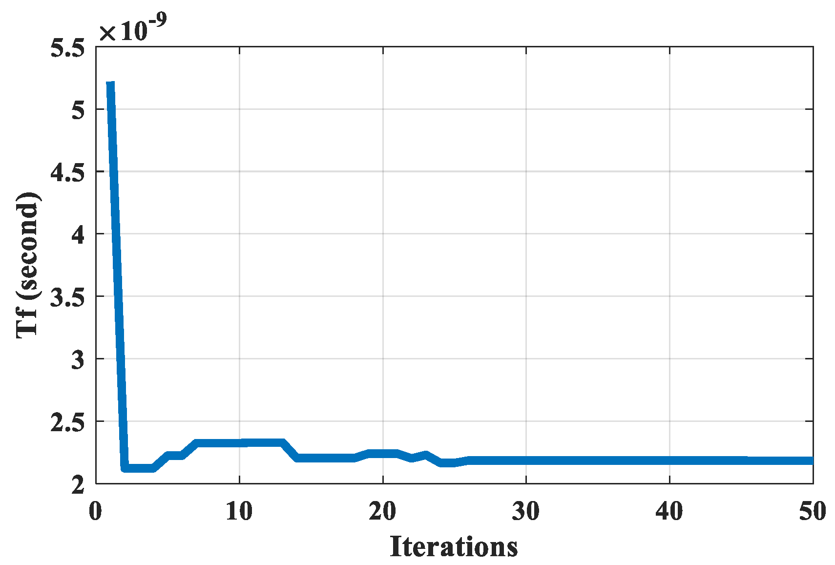
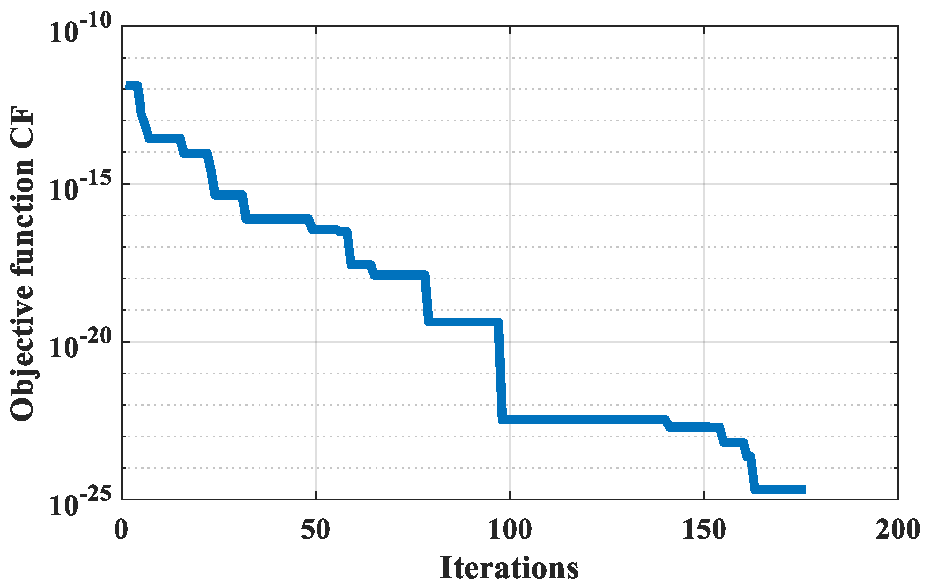
Figure 4 shows the convergence of the objective function, given in 13, with the iterations for the seventh design set. In Figure 4, it can be seen that the objective function reaches an optimal value of 2.7473019 × 10²⁰ s. The 7th design set wass chosen since it has the lowest value of the cost function.
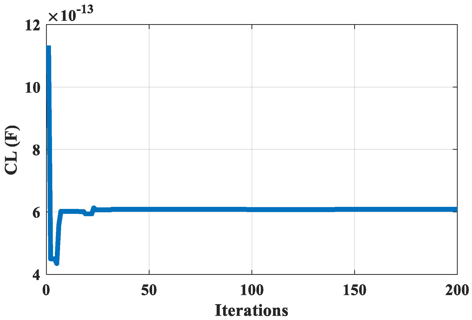
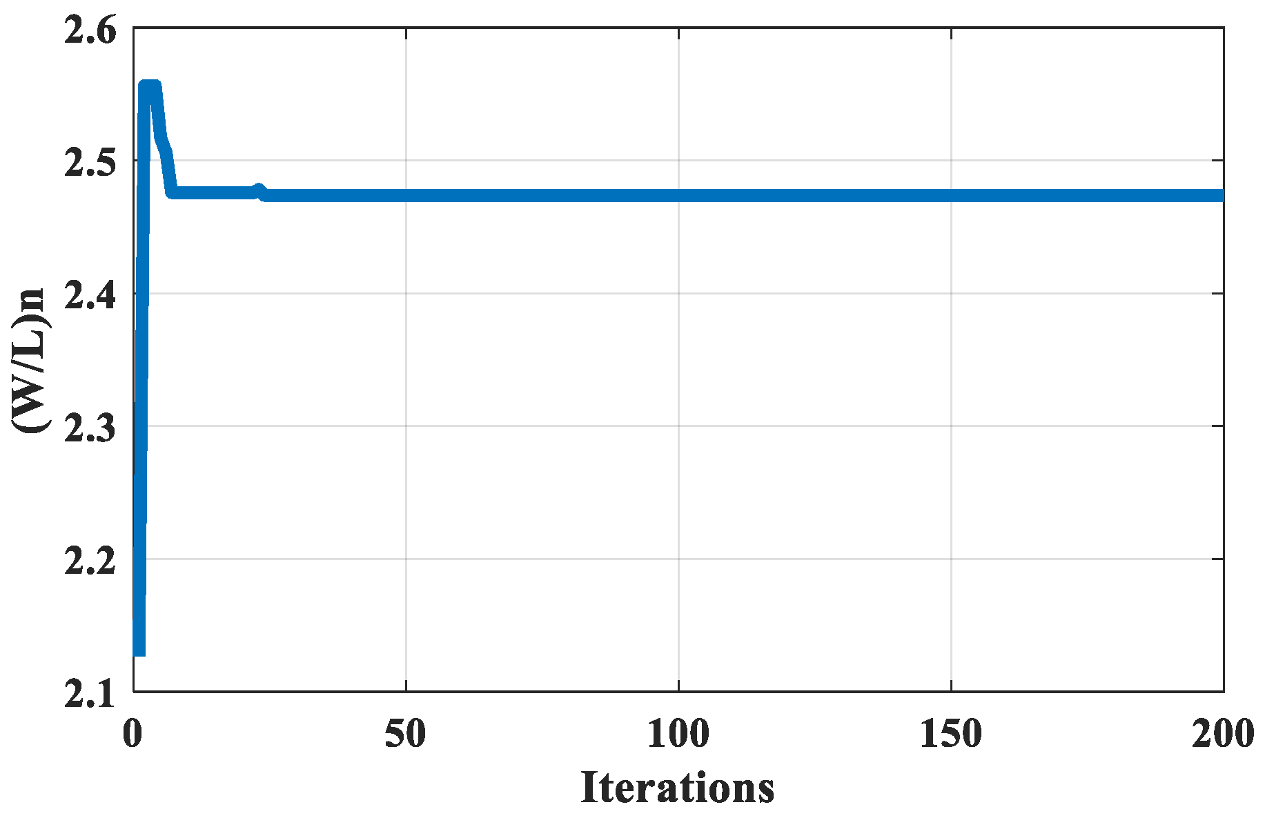
 Figure 5, Figure 6 and Figure 7 show the convergence plots of the inverter design parameters, CL, (W/L), and (tf), for the same design set. In Figure 5, the optimum value for the load capacitance is 0.7122034 pF and it starts to converge after 24 iterations. The aspect ratio (W/L) optimum value for the seventh set is shown in Figure 3 to be equal to 1.8113496. The optimum value for the fall time is equal to 2.1820107 ns as shown in Figure 7.
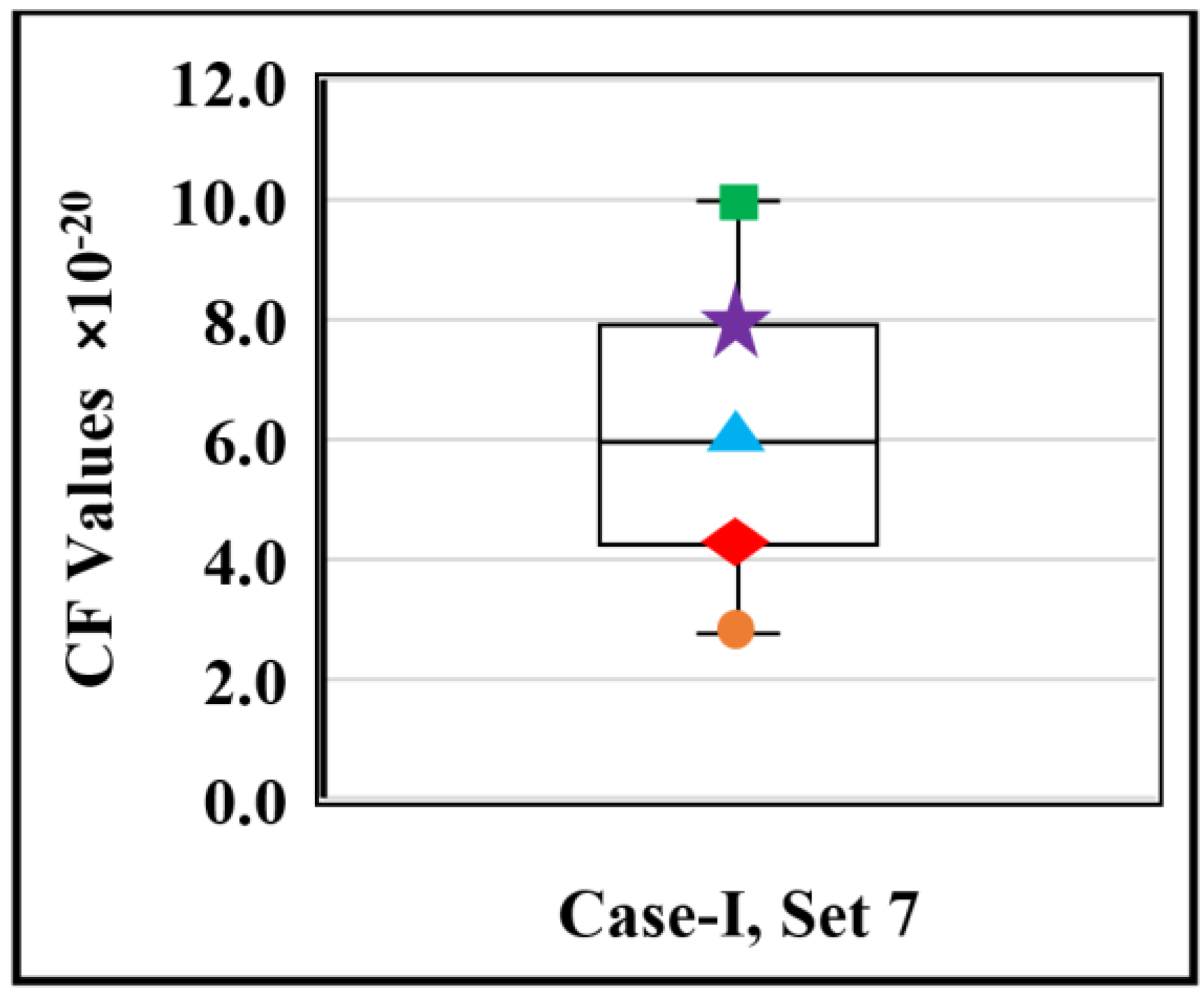
The MA is stochastic by its nature. Therefore, different simulation runs will give different design results. The MA has been run 50 times for the best design set of all the case studies and the resulting CF values have been utilized for the box and whisker plots. Figure 8 shows the box and whisker plot for the seventh design set of the MA; the green square represents the maximum value, the purple star represents upper whisker, the blue triangle represents median value, the red diamond represents the lower whisker, and the orange circle represents the minimum value. The median value of the CF is found to be equal to 5.95 × 10²⁰, the maximum value is 9.98 × 10²⁰, and the minimum value is 2.75 × 10²⁰, the lower whisker is 4.32594 × 10²⁰ and the upper whisker is 7.8561 × 10²⁰.
Table 5 shows the simulation results for each design set in case studies I. Spice simulation results show that the MA method is very accurate with small variations due to MOSFET junction capacitance.
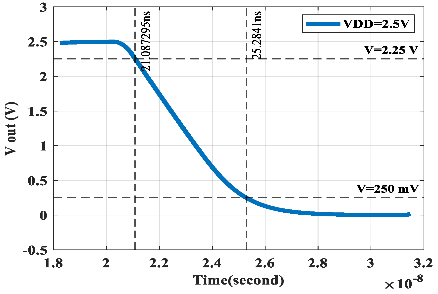
The fall time for the seventh design set of Case I using Spice simulation is shown in Figure 9. As shown in Figure 9, using the values obtained using the MA, an optimum value of the fall time equal to 4.1925571 ns is achieved.
For Case II, the optimal CMOS inverter design with symmetrical operation (fall time equals rise time) is found using the MA for the eight different design sets in Table 2. The MA gives the optimal design parameters needed to minimize the cost function in 15. Table 6 gives the optimal design parameters needed for the CMOS inverter with a symmetrical operation for the eight design sets of Case II. It is apparent that in Table 6 the symmetry in the fall time and rise time has been achieved.
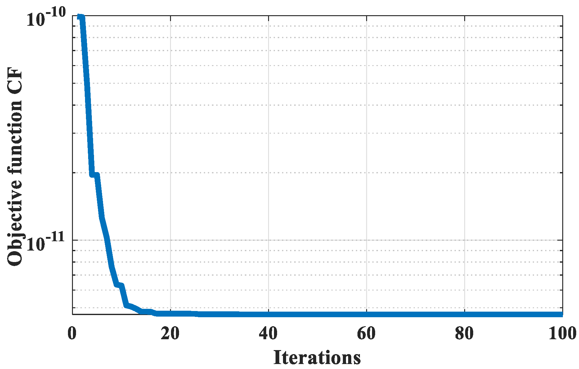
In Figure 10, a plot of the objective function convergence with MA iteration for the fourth design set is shown; the objective function converges after 160 iterations. Figure 10, Figure 11 and Figure 12 show the convergence plots of the inverter design parameters, CL, (W/L)n, and (W/L)p, for the same design set. In Figure 11, convergence is achieved after the 25th iteration with an optimum value of 0.6085469 pF for the load capacitance. 
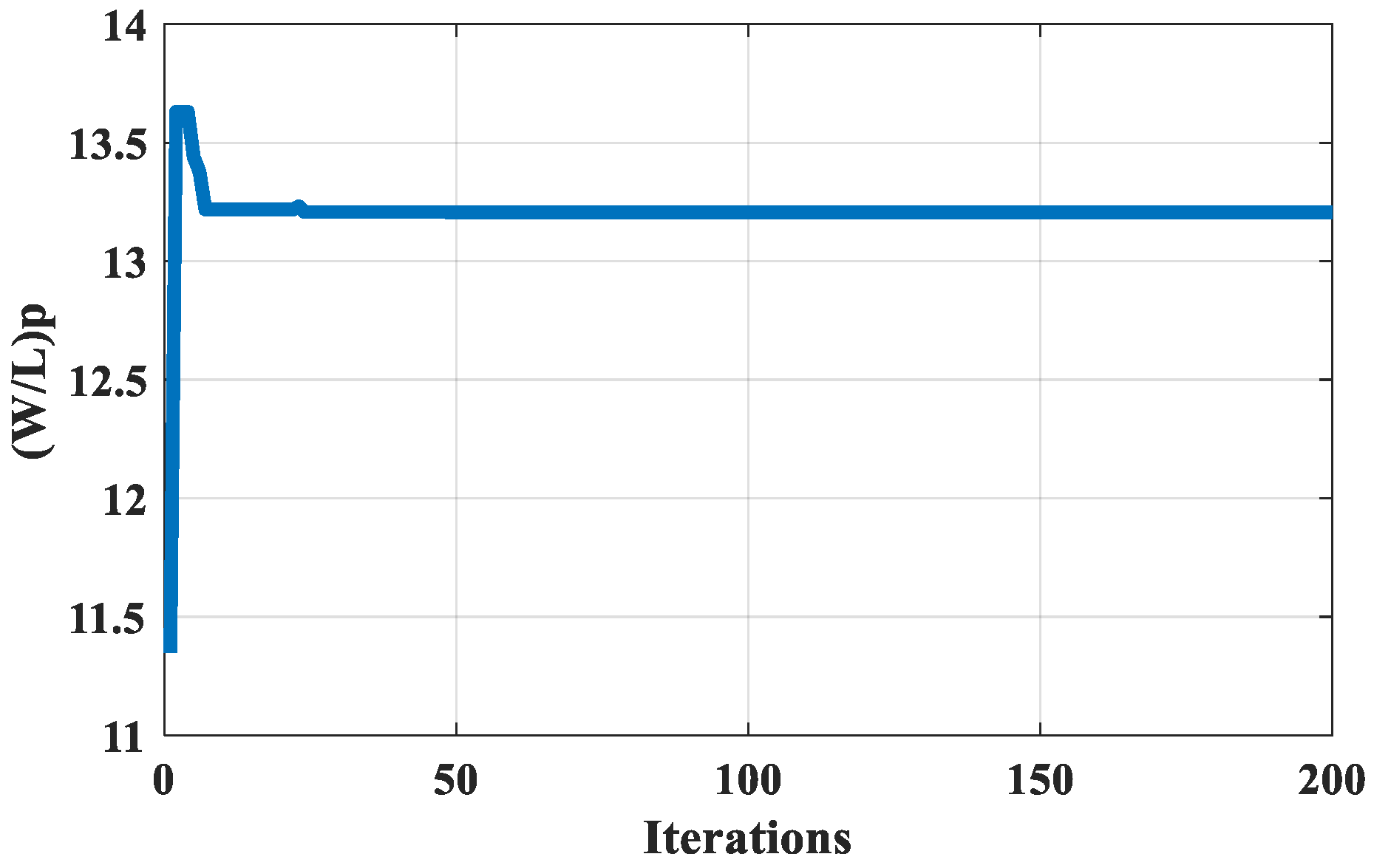
Figure 12 shows the convergence of the NMOS transistor aspect ratio for the fourth set which is equal to 2.4734372. On the other hand, the optimum value for PMOS aspect ratio is equal to 13.206141, as shown in Figure 13.
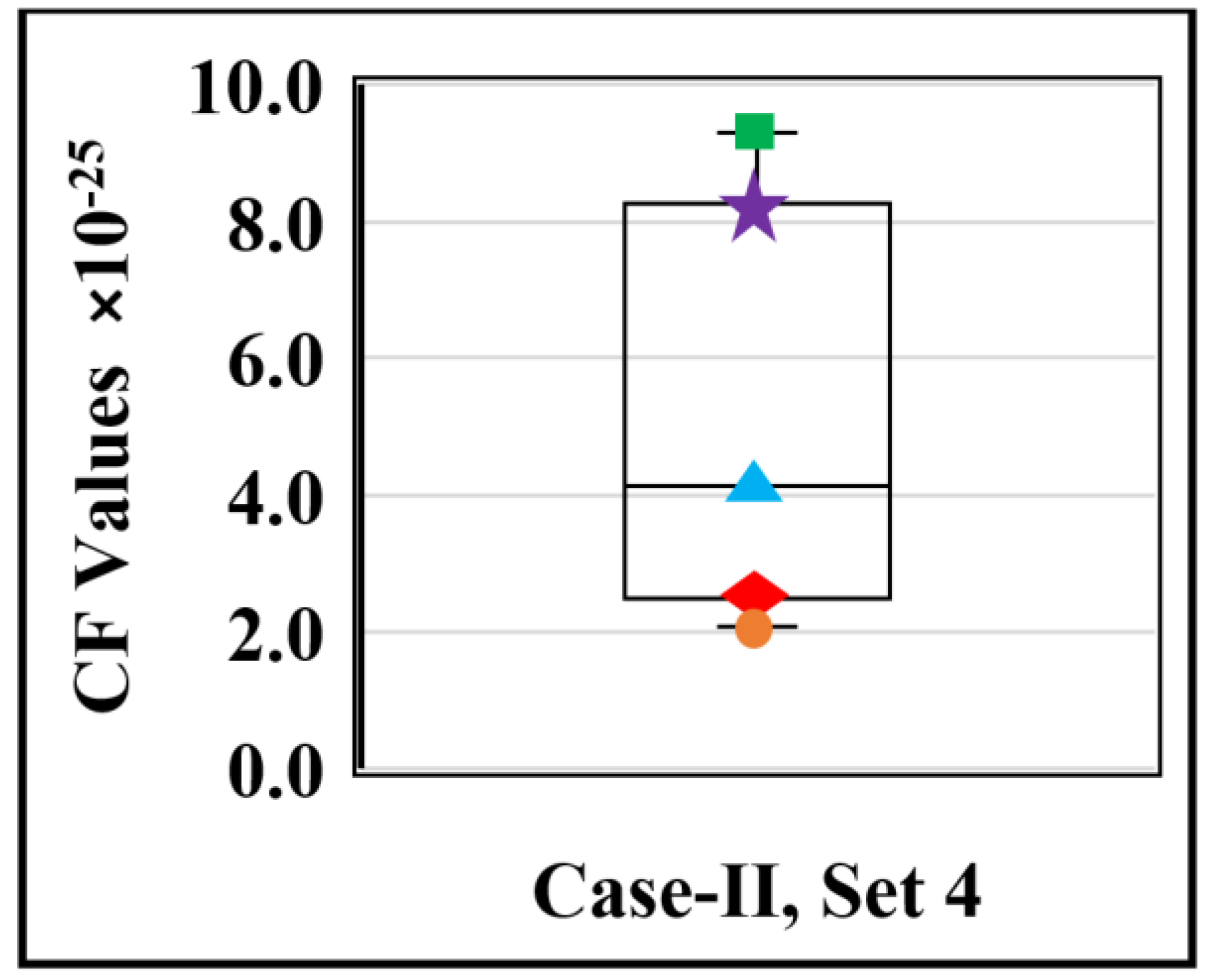
Figure 14 shows the box and whisker plot for the fourth design set of Case II. The green square represents the maximum value, the purple star represents upper whisker, the blue triangle represents median value, the red diamond represents the lower whisker, and the orange circle represents the minimum value. The median value is found to be 4.14 × 1025, the maximum value is 9.31 × 1025, the minimum value is 2.07 × 1025, the lower whisker is 2.6366 × 1025, and the upper whisker is 8.2718 × 1025.
Table 7 shows the simulation results for each design set in case studies II. Spice simulation results show that the MA method is very accurate with small variations due to MOSFET junction capacitance.
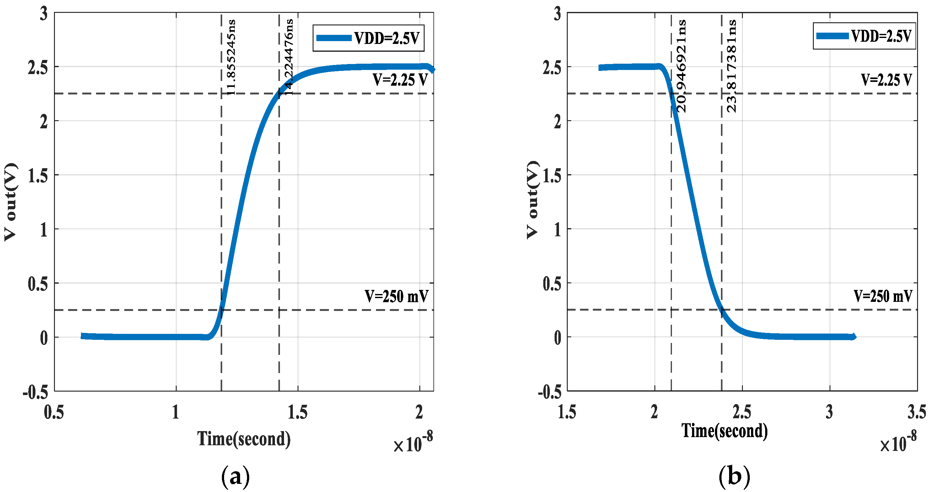
The rise and fall times for the fourth design set of Case II using Spice simulation are shown in Figure 15. Spice simulations in Figure 15 show that the designed inverter has a al fall time and rise time with only fractions of nano second difference.
In Case III, the optimal CMOS inverter design for each design set in Table 3 is found using the MA with population size (males and females) equals 20 and 100 iterations. The results give the optimal design parameters. (W/L)p, (W/L)n, and CL of the CMOS inverter, which minimizes the objective function given in Equation (21). Then, these optimal values of the CMOS inverter parameters are used to calculate the fall time (tf), the rise time (tr), and the propagation delay times (tPHL and tPLH). Table 8 summarizes the results obtained using the MA for each design set in Case III, which satisfies the symmetrical output waveform with equal rise and fall times, and the symmetrical propagation delay time (tPHL equal tPLH).
Table 9 shows a comparison of the MA results with results obtained by different optimization algorithms. The optimal value of the CF (in ps) of the MA is compared to the optimal value of CF using PSOCFIWA [25], DE [26], ALC-PSO [29], CRPSO [27], PSO [30], HS–DE [32], and SOS [32]. The results show that the suggested MA outperforms most of the widely used optimization methods in finding the optimal CMOS inverter design with the lowest CF value.
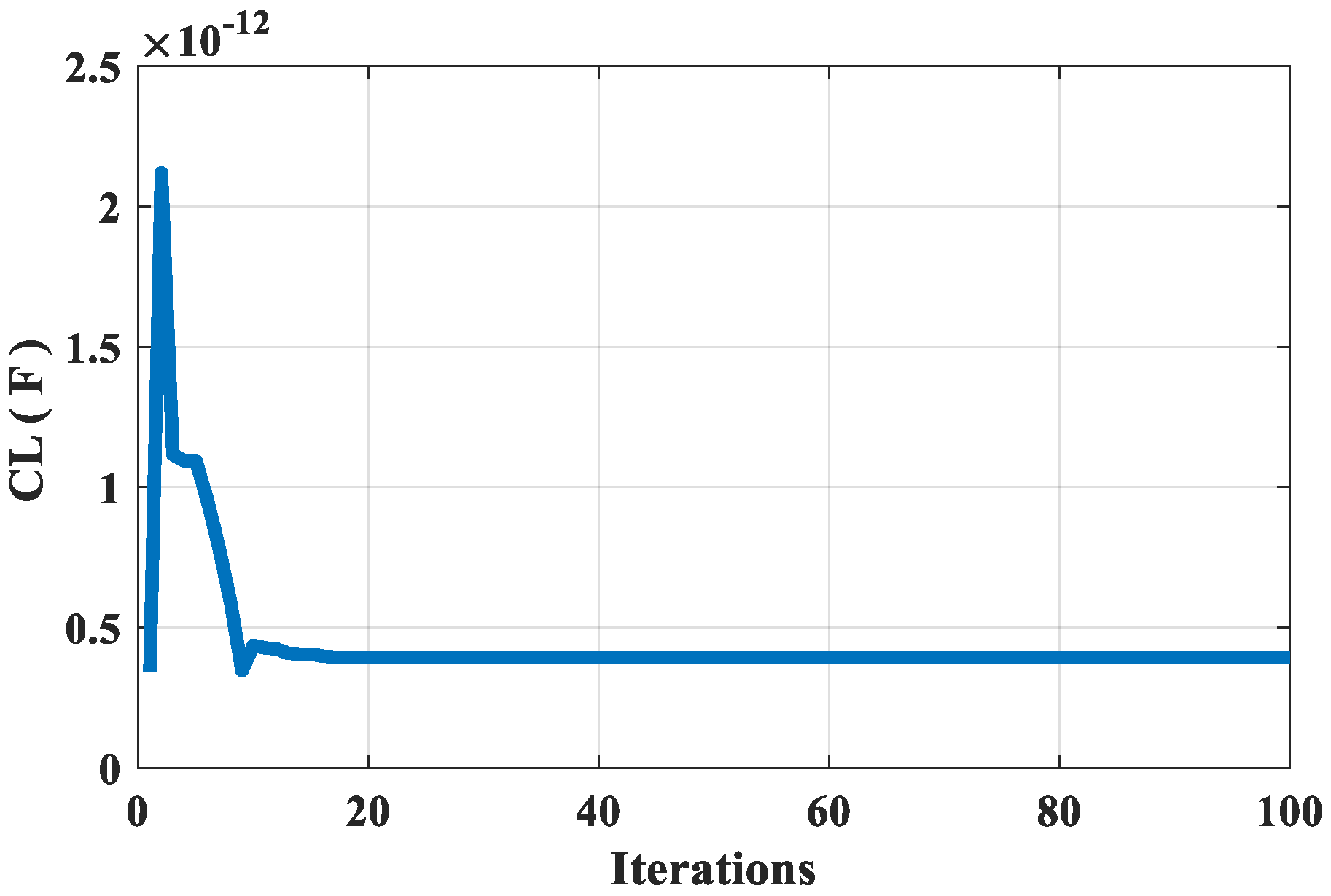
Figure 16 shows the convergence plot of the objective function for the eighth design set. The optimum value of the objective function is 4.67217 ps and it converges after 18 iterations. Figure 17, Figure 18 and Figure 19 show the convergence plots of the inverter design parameters: CL, (W/L)n and (W/L)p for the same design set. 
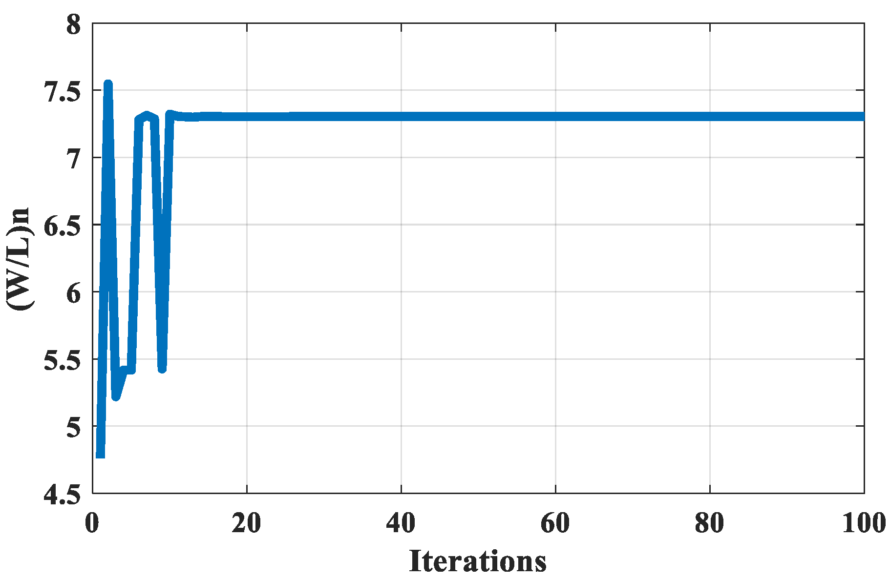
Figure 17 shows that the capacitance load optimum value for the eighth set is equal to 0.394871 pF. The aspect ratio for the NMOS transistor converges at a value of 7.30448 after 16 iterations as shown in Figure 18. On the other hand, 
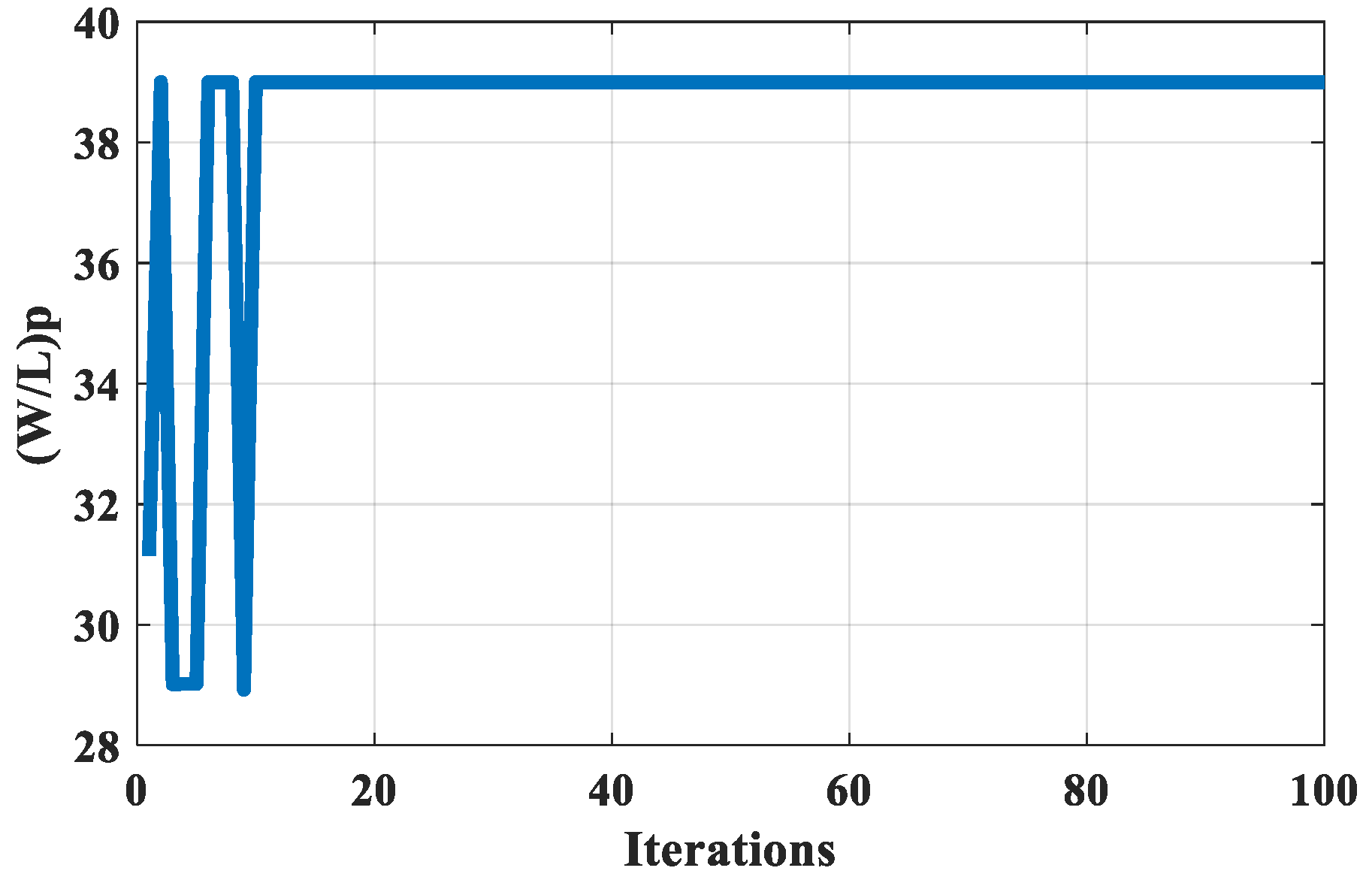
Figure 19 shows that the optimum aspect ratio for the PMOS transistor is 39.
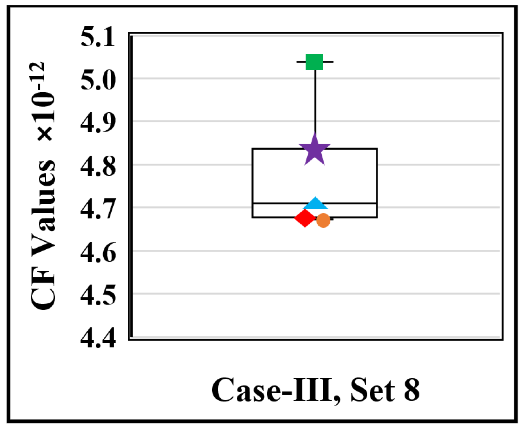
Figure 20 shows the box and whisker plot for the eighth design set of the MA. The green square represents the maximum value, the purple star represents upper whisker, the blue triangle represents median value, the red diamond represents the lower whisker, and the orange circle represents the minimum value.
The median value is found to be 4.71 × 10¹², the maximum value is 5.04 × 10¹², the minimum value is 4.67 × 10¹², the lower whisker is 4.67727 × 10¹², and the upper whisker is 4.81995 × 10¹².
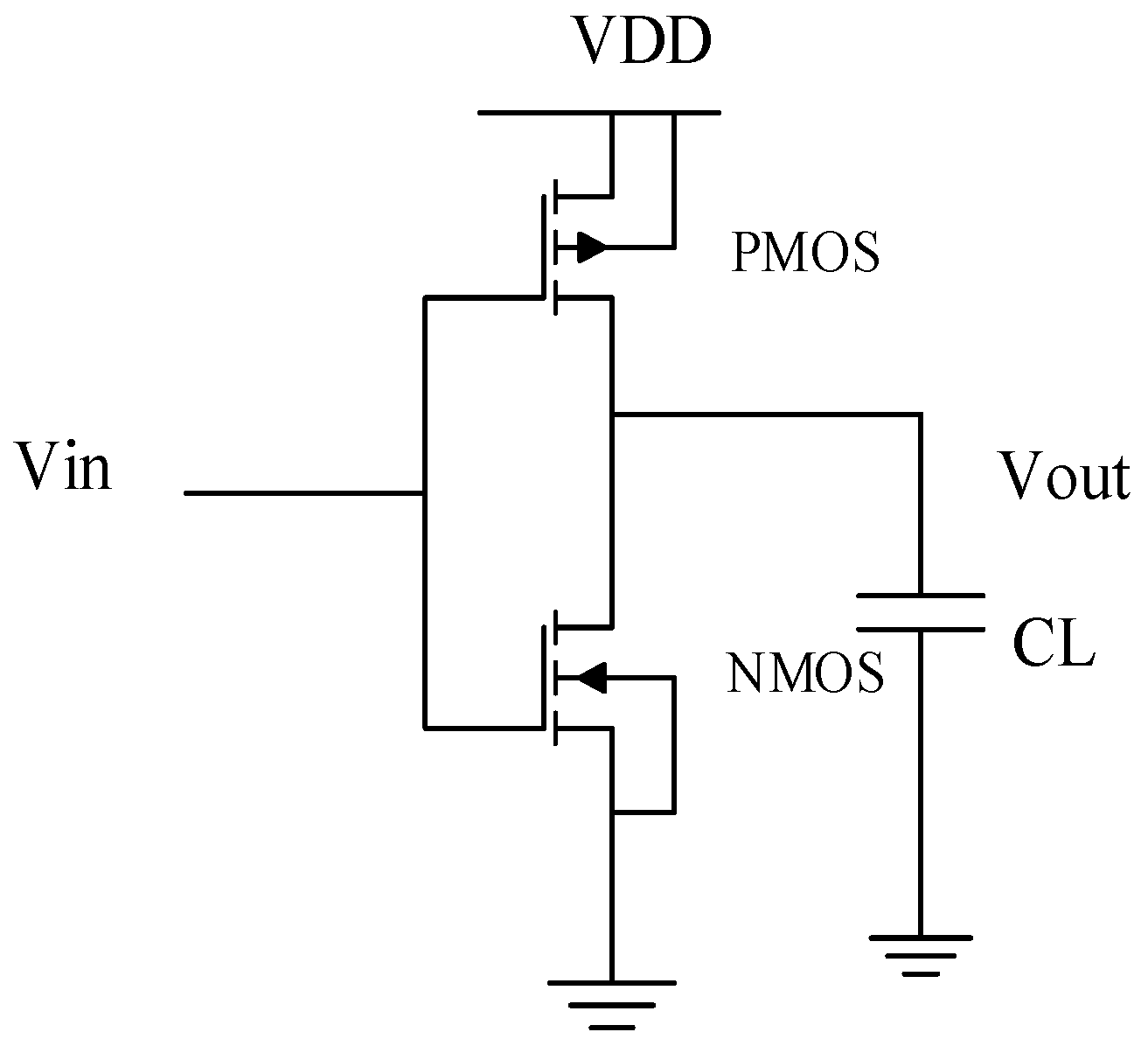
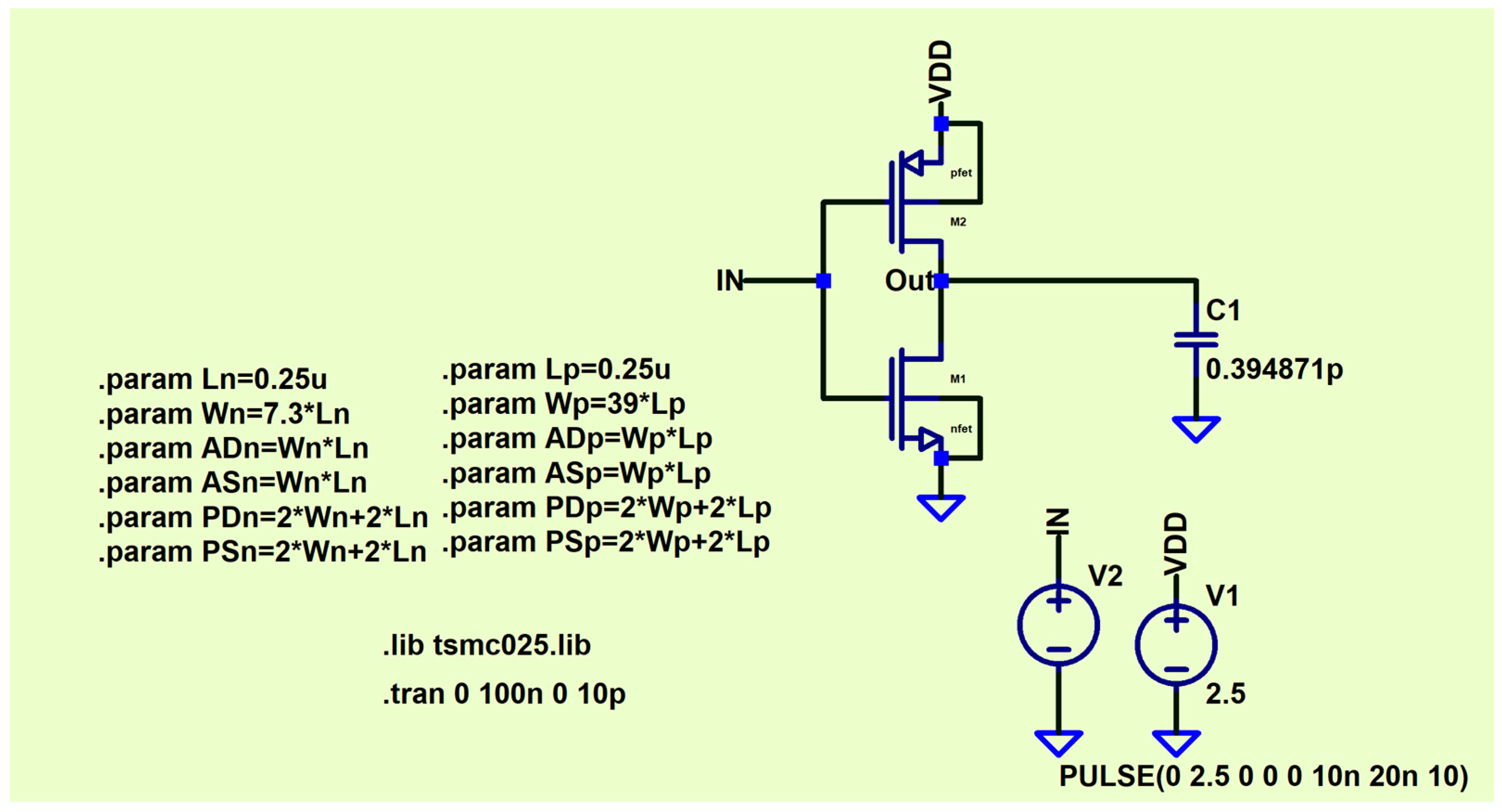
To verify the results obtained using MA optimization, the optimal values of the design parameters are used in the inverter Spice simulations. The simulated circuit is shown in Figure 21. Table 10 shows the simulation results for each design set in the three case studies. Spice simulation results show that the MA method is very accurate with small variations due to MOSFET junction capacitance.
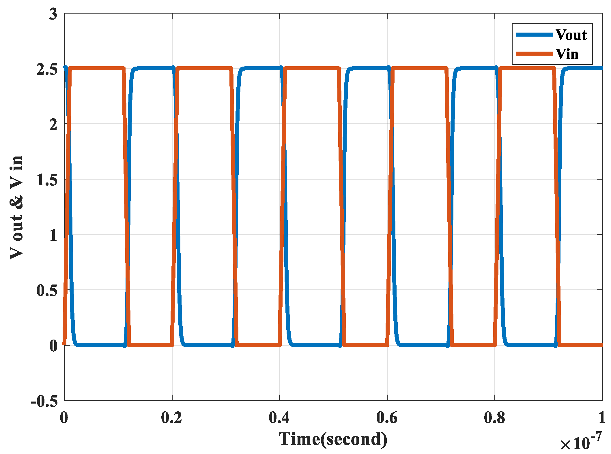
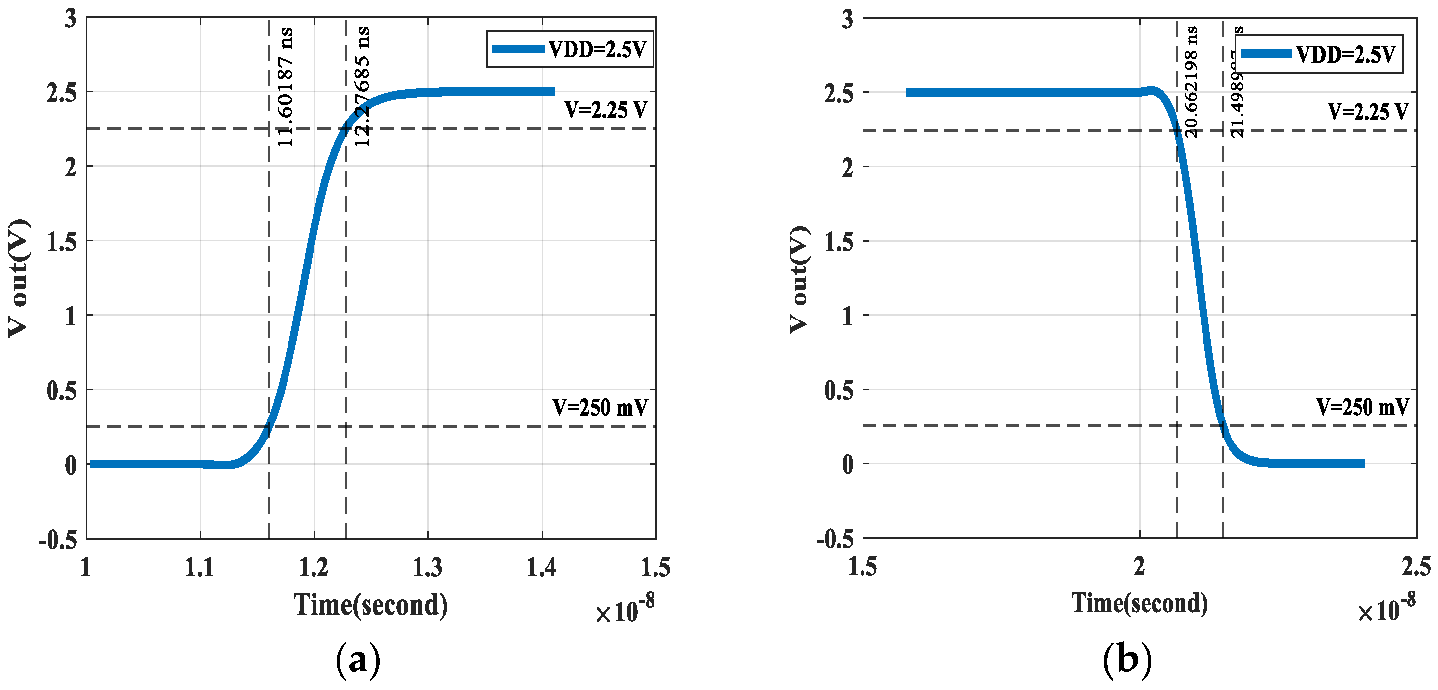
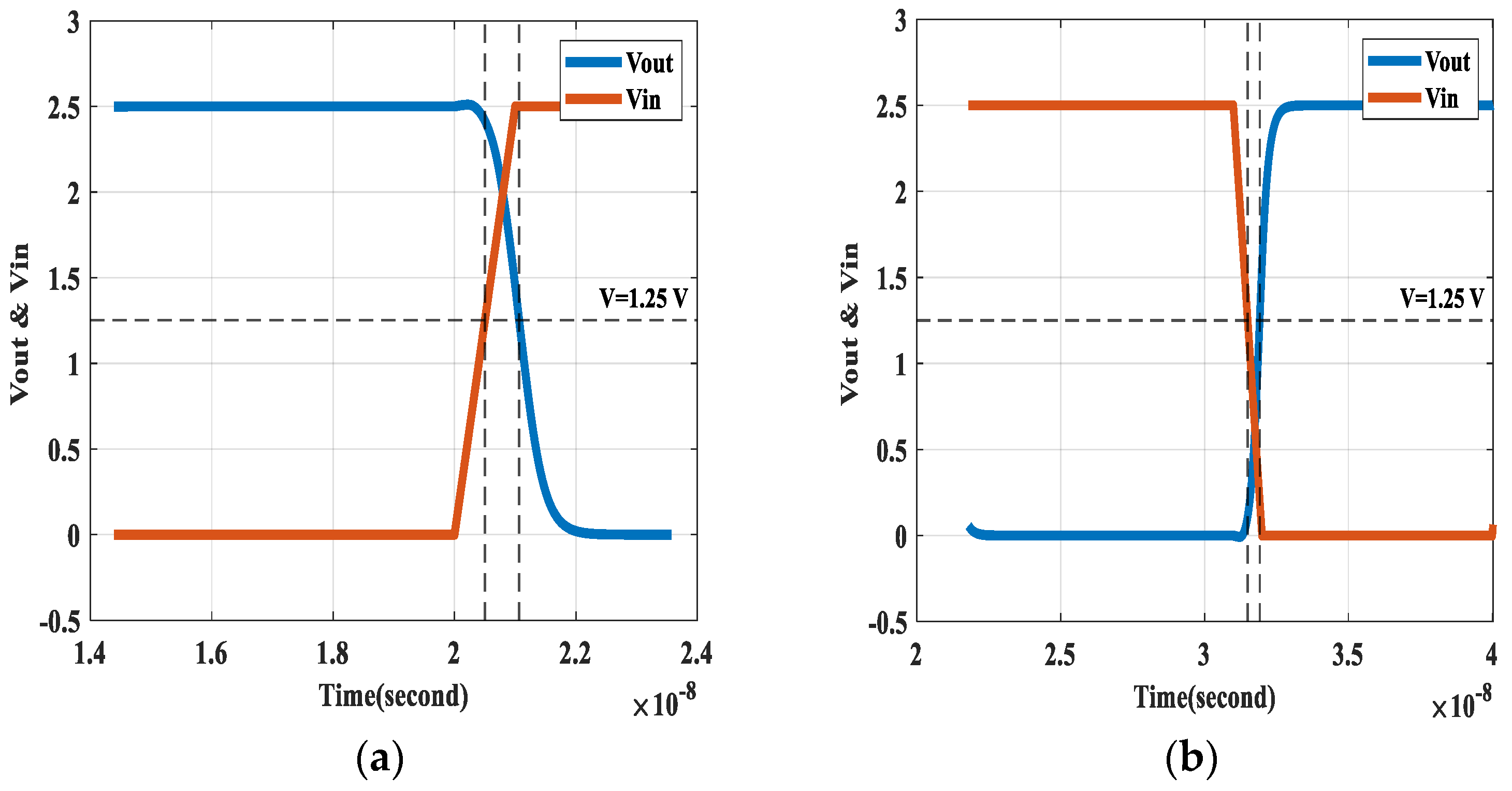
Spice simulations for the rise and fall times and the propagation delay times for the eighth design set of Case III are shown in Figure 22 and Figure 23, respectively. Rise time and fall time in Figure 22 are 0.840474 ns and 0.6761915 ns with a difference less than 0.2 ns. propagation delay high to low and low to high for the eighth set are shown in Figure 23 to be equal to 0.565393 ns and 0.416783 ns, respectively.

6. Conclusions

This paper employs the Mayfly Algorithm (MA), one of the latest optimization algorithms, to find the optimal design of the CMOS inverter. The design problem is mathematically formulated as an optimization problem. Three case studies with different constraints and design criteria are presented to illustrate the effectiveness of the proposed optimization algorithm to find the global solution of the objective function. The results of the three case studies were used in the spice simulations in order to verify the results. In Case I, estimating of the fall time is found depending on the design parameters and 0.25 µm TSMC CMOS technology manufacturing parameters. Case I is performed for eight different sets with different ranges of design parameters and design criteria. The results show compatibility between MA results and Spice results. The maximum fall time difference between Mayfly Algorithm and Spice Simulation for all design sets is equal to 2.075711 ns. In the second case, the goal is to design an inverter with symmetrical fall and rise times. In Case II, the MA is performed for eight design sets. The difference between the fall time and rise time is minimized as shown Spice simulations, where the maximum difference between fall time and rise time is equal to 0.9784731 ns. In Case III, the CMOS inverter is designed to achieve a symmetrical fall time and rise time and a symmetrical propagation delay time. Spice simulations show that symmetry was achieved in Case III with minimum difference equal to 0.312893 ns and maximum difference equal to 1.076540 ns. Negligible variations between the MA outcomes and the spice results are observed due to more complicated models used in Spice simulations compared to the theoretical mathematical equations used in the optimization method. When comparing optimization methods, the MA contains very simple approximate expressions, and it has fast convergence and a better chance to find the global best solution of the cost function.
The values of the width to length ratio have to be slightly modified to meet design rules for the process technology used in fabricating the circuit. This modification will have an almost negligible effect on the rise and fall times. In the future, more work will be conducted to identify the optimal width to length ratio of CMOS transistors used in a CMOS inverter to achieve the minimum power dissipation and time delay. Achieving this optimal ratio is critical for developing more energy-efficient and high-performance electronic devices. The Mayfly Algorithm can not only help in optimizing the CMOS inverter but can also be extended to optimize more complex circuits, such as Schmitt trigger circuits. Schmitt trigger circuits are commonly used in applications such as signal processing, noise filtering, and waveform generation.

Author Contributions

Conceptualization, F.N.Z.; Methodology, A.A.; Software, F.N.Z.; Validation, H.A.; Formal Analysis, F.N.Z. and H.A.; Investigation, A.A. and H.A.; Resources, F.N.Z.; Data Curation, H.A.; Writing-Original Draft Preparation, F.N.Z. and H.A.; Writing-Review & Editing, A.A. and F.N.Z.; Visualization, A.A.; Supervision, F.N.Z.; Project Administration, F.N.Z. All authors have read and agreed to the published version of the manuscript.

Funding

This research was funded by the Deanship of Research at Jordan University of Science and Technology. Grant number: 20220336. Sponsor’s website: Jordan University of Science and Technology (just.edu.jo) (https://www.just.edu.jo/Pages/Default.aspx, accessed on 29 April 2023).

Data Availability Statement

Not applicable.

Acknowledgments

The author would like to thank the Deanship of Research at Jordan University of Science and Technology for supporting this work.

Conflicts of Interest

The authors declare no conflict of interest.

References

  1. Liu, X.; Yang, J.; Li, J.; Lin, F.; Li, B.; Zhang, Z.; He, W.; Huang, M. GaN-Based GAA Vertical CMOS Inverter. IEEE J. Electron. Devices Soc. 2022, 10, 224–228. [Google Scholar] [CrossRef]
  2. Rawat, A.; Gupta, A.K.; Rawat, B. Performance Projection of 2-D Material-Based CMOS Inverters for Sub-10-nm Channel Length. IEEE Trans. Electron Devices 2021, 68, 3622–3629. [Google Scholar] [CrossRef]
  3. Verma, S.; Paul, R.; Shukla, M. Non-Volatile Latch Compatible With Static and Dynamic CMOS for Logic in Memory Applications. IEEE Trans. Magn. 2022, 58, 3400308. [Google Scholar] [CrossRef]
  4. Tripathi, J.N.; Arora, P.; Shrimali, H.; Achar, R. Efficient Jitter Analysis for a Chain of CMOS Inverters. IEEE Trans. Electromagn. Compat. 2020, 62, 229–239. [Google Scholar] [CrossRef]
  5. Zghoul, F.N.; Ay, S.U.; Ababneh, A. Gain and offset analysis of comparator using the bisection theorem and a balanced method. Int. J. Electron. 2016, 103, 1965–1983. [Google Scholar] [CrossRef]
  6. Zghoul, F.N.; Ay, S.U.; Saadeh, O.S. Protraction of Bartlett Bisection Theorem to Cross Coupled Circuits. J. Eng. Appl. Sci. 2017, 12, 7104–7111. [Google Scholar]
  7. Bhattacharjee, P.; Bhattacharyya, B.K.; Majumder, A. A Vector-Controlled Variable Delay Circuit to Develop Near-Symmetric Output Rise/Fall Time. Circuits Syst Signal Process 2021, 40, 1569–1588. [Google Scholar] [CrossRef]
  8. Cortadella, J.; Sapatnekar, S.S. Static timing analysis. In Electronic Design Automation for IC Implementation, Circuit Design, and Process Technology: Circuit Design, and Process Technology; CRC Press: Boca Raton, FL, USA, 2016; p. 133. [Google Scholar]
  9. Saint, C.; Saint, J. IC Mask Design: Essential Layout Techniques; McGraw-Hill: New York, NY, USA, 2002. [Google Scholar]
  10. Dwivedi, A.K.; Guduri, M.; Mehra, R.; Islam, A. A monotonic digitally controlled delay element-based programmable trigger pulse generator. In Proceedings of the Second International Conference on Computer and Communication Technologies; Springer: New Delhi, India, 2016; pp. 365–374. [Google Scholar]
  11. Geiger, R.L.; Allen, P.E.; Strader, N.R. Vlsi Design Techniques for Analog and Digital Circuits; McGraw-Hill Publishing Company: New York, NY, USA, 1990. [Google Scholar]
  12. Ul Ain, Q. Osman Hasan Timing Analysis of Digital Circuits. PhD Thesis, School of Electrical Engineering and Computer Science, National University of Sciences and Technology, Islamabad, Pakistan, 2018. [Google Scholar]
  13. Raja, T.; Agrawal, V.D.; Bushnell, M.L. Variable input delay cmos logic for low power design. IEEE Trans. Very Large Scale Integr. (VLSI) Syst. 2009, 17, 1534–1545. [Google Scholar] [CrossRef]
  14. Morales, J.I.; Chierchie, F.; Mandolesi, P.S.; Paolini, E.E. A high-resolution all-digital pulse-width modulator architecture with a tunable delay element in CMOS. Int. J. Circuit Theory Appl. 2020, 48, 1329–1345. [Google Scholar] [CrossRef]
  15. Stanimirović, P.S.; Shaini, B.I.; Sabi’u, J.; Shah, A.; Petrović, M.J.; Ivanov, B.; Cao, X.; Stupina, A.; Li, S. Improved Gradient Descent Iterations for Solving Systems of Nonlinear Equations. Algorithms 2023, 16, 64. [Google Scholar] [CrossRef]
  16. Zhao, H.; Wang, Y.; Zhao, M.; Sun, C.; Tan, Q. Application of Gradient Descent Continuous Actor-Critic Algorithm for Bilateral Spot Electricity Market Modeling Considering Renewable Power Penetration. Algorithms 2017, 10, 53. [Google Scholar] [CrossRef]
  17. Huang, S.; Tsai, Y.-C.; Chou, F.-D. A Trajectory-Based Immigration Strategy Genetic Algorithm to Solve a Single-Machine Scheduling Problem with Job Release Times and Flexible Preventive Maintenance. Algorithms 2023, 16, 207. [Google Scholar] [CrossRef]
  18. Bulut, O.; Gorgun, G.; Wongvorachan, T.; Tan, B. Rapid Guessing in Low-Stakes Assessments: Finding the Optimal Response Time Threshold with Random Search and Genetic Algorithm. Algorithms 2023, 16, 89. [Google Scholar] [CrossRef]
  19. Zhou, C.; Liu, X.; Xu, F. Design Optimization of Steering Mechanisms for Articulated Off-Road Vehicles Based on Genetic Algorithms. Algorithms 2018, 11, 22. [Google Scholar] [CrossRef]
  20. Saqib, N.; Haque, K.F.; Yanambaka, V.P.; Abdelgawad, A. Convolutional-Neural-Network-Based Handwritten Character Recognition: An Approach with Massive Multisource Data. Algorithms 2022, 15, 129. [Google Scholar] [CrossRef]
  21. Vural, R.A.; Der, O.; Yildirim, T. Particle Swarm Optimization Based Inverter Design Considering Transient Performance. Digit. Signal Process. 2010, 20, 1215–1220. [Google Scholar] [CrossRef]
  22. Vural, R.A.; Der, O.; Yildirim, T. Investigation of Particle Swarm Optimization for Switching Characterization of Inverter Design. Expert Syst. Appl. 2011, 38, 5696–5703. [Google Scholar] [CrossRef]
  23. Mukhopadhyay, J.; Pandit, S. Modeling and Design of a Nano Scale CMOS Inverter for Symmetric Switching Characteristics. VLSI Des. 2012, 2012, 505983. [Google Scholar] [CrossRef]
  24. Gayathri, P.; Sateesh, K.; Srikanth, G. Design of A Nano-Scale CMOS Inverter with Symmetric Switching Characteristics using Particle Swarm Optimization Algorithm. Int. J. VLSI Syst. Des. Commun. Syst. 2015, 3, 1330–1334. [Google Scholar]
  25. De, B.P.; Kar, R.; Mandal, D.; Ghoshal, S.P. Design of Symmetric Switching CMOS Inverter using PSOCFIWA. In Proceedings of the 2014 International Conference on Communication and Signal Processing, Melmaruvathur, India, 3–5 April 2014; pp. 1818–1824. [Google Scholar]
  26. De, B.P.; Kar, R.; Mandal, D.; Ghoshal, S.P. Optimal CMOS Inverter Design using Differential Evolution Algorithm. J. Electr. Syst. Inf. Technol. 2015, 2, 219–241. [Google Scholar] [CrossRef]
  27. De, B.P.; Kar, R.; Mandal, D.; Ghoshal, S.P. Optimal High Speed CMOS Inverter Design using Craziness Based Particle Swarm Optimization Algorithm. Open Eng. 2015, 5, 256–273. [Google Scholar] [CrossRef]
  28. De, B.P.; Kar, R.; Mandal, D.; Ghoshal, S.P. Optimal Design of High Speed Symmetric Switching CMOS Inverter using Hybrid Harmony Search with Differential Evolution. Soft Comput. 2016, 20, 3699–3717. [Google Scholar] [CrossRef]
  29. De, B.P.; Kar, R.; Mandal, D.; Ghoshal, S.P. PSO with Aging Leader and Challengers for Optimal Design of High Speed Symmetric Switching CMOS Inverter. Int. J. Mach. Learn. Cybern. 2017, 8, 1403–1422. [Google Scholar] [CrossRef]
  30. Kumar, M.; Rawat, T.K.; Majhi, A. Design of Symmetric Switching CMOS Inverter using Cuckoo Search Algorithm. In Proceedings of the 2016 IEEE 1st International Conference on Power Electronics, Intelligent Control and Energy Systems (ICPEICES), Delhi, India, 4–6 July 2016; pp. 1–6. [Google Scholar] [CrossRef]
  31. Zafarkhah, E.; Maymandi-Nejad, M.; Zare, M. Improved Accuracy Equation for Propagation Delay of a CMOS Inverter in a Single Ended Ring Oscillator. AEU-Int. J. Electron. Commun. 2017, 71, 110–117. [Google Scholar] [CrossRef]
  32. Dib, N.; Al-Sammarraie, U. Optimal Design of Symmetric Switching CMOS Inverter using Symbiotic Organisms Search Algorithm. Int. J. Electr. Comput. Eng. 2020, 10, 171–179. [Google Scholar] [CrossRef]
  33. Kumar, S.; Tejani, G.G.; Pholdee, N.; Bureerat, S. Multi-Objective Modified Heat Transfer Search for Truss Optimization. Eng. Comput. 2021, 37, 3439–3454. [Google Scholar] [CrossRef]
  34. Zervoudakis, K.; Tsafarakis, S. A Mayfly Optimization Algorithm. Comput. Ind. Eng. 2020, 145, 106559. [Google Scholar] [CrossRef]
  35. Gao, Z.-M.; Zhao, J.; Li, S.-R.; Hu, Y.-R. The Improved Mayfly Optimization Algorithm. J. Phys. Conf. Ser. 2020, 1684, 12077. [Google Scholar] [CrossRef]
  36. Elavarasan, G.; Kumar, K.S.; Marimuthu, M.; Narayanasamy, K.; Selvam, R.P. Evolutionary Oppositional Mayfly Optimization Based Task Scheduling Algorithm for Cloud Computing. Turk. J. Physiother. Rehabil. 2021, 32, 3800–3806. [Google Scholar]
  37. Zhao, J.; Gao, Z.-M. The Negative Mayfly Optimization Algorithm. J. Phys. Conf. Ser. 2020, 1693, 12098. [Google Scholar] [CrossRef]
  38. Bhattacharyya, T.; Chatterjee, B.; Singh, P.K.; Yoon, J.H.; Geem, Z.W.; Sarkar, R. Mayfly in Harmony: A New Hybrid Meta-Heuristic Feature Selection Algorithm. IEEE Access 2020, 8, 195929–195945. [Google Scholar] [CrossRef]
  39. Liu, Y.; Chai, Y.; Liu, B.; Wang, Y. Bearing Fault Diagnosis Based on Energy Spectrum Statistics and Modified Mayfly Optimization Algorithm. Sensors 2021, 21, 2245. [Google Scholar] [CrossRef] [PubMed]
  40. Guo, X.; Yan, X.; Jermsittiparsert, K. Using the Modified Mayfly Algorithm for Optimizing the Component Size and Operation Strategy of a High Temperature PEMFC-Powered CCHP. Energy Rep. 2021, 7, 1234–1245. [Google Scholar] [CrossRef]
  41. Elaziz, M.A.; Senthilraja, S.; Zayed, M.E.; Elsheikh, A.H.; Mostafa, R.R.; Lu, S. A New Random Vector Functional Link Integrated with Mayfly Optimization Algorithm for Performance Prediction of Solar Photovoltaic Thermal Collector Combined with Electrolytic Hydrogen Production System. Appl. Therm. Eng. 2021, 193, 117055. [Google Scholar] [CrossRef]
  42. Park, J.-B.; Lee, K.-S.; Shin, J.-R.; Lee, K.Y. A Particle Swarm Optimization for Economic Dispatch with Nonsmooth Cost Functions. IEEE Trans. Power Syst. 2005, 20, 34–42. [Google Scholar] [CrossRef]
Figure 1. Flowchart of the MA [36].
Algorithms 16 00237 g001
Figure 2. CMOS inverter circuit.
Algorithms 16 00237 g002
Figure 3. Voltage waveforms of the CMOS inverter.
Algorithms 16 00237 g003
Figure 4. MA results for the seventh design set of Case I.
Algorithms 16 00237 g004
Figure 5. Plot of CL with iterations for the seventh design set of Case I.
Algorithms 16 00237 g005
Figure 6. Plot of (W/L) with iterations for the seventh design set of Case I.
Algorithms 16 00237 g006
Figure 7. Plot of tf with iterations for the seventh design set of Case I.
Algorithms 16 00237 g007
Figure 8. Box and whisker plot of the MA for the seventh design set of Case I.
Algorithms 16 00237 g008
Figure 9. Fall time using Spice for the seventh design set of Case I.
Algorithms 16 00237 g009
Figure 10. The MA results for the fourth design set of Case II.
Algorithms 16 00237 g010
Figure 11. Plot of CL with iterations for the fourth design set of Case II.
Algorithms 16 00237 g011
Figure 12. Plot of (W/L)n with iterations for the fourth design set of Case II.
Algorithms 16 00237 g012
Figure 13. Plot of (W/L)p with iterations for the fourth design set of Case II.
Algorithms 16 00237 g013
Figure 14. Box and whisker plot of the MA for the fourth design set of Case II.
Algorithms 16 00237 g014
Figure 15. Spice simulation for the fourth design set of Case II. (a) Rise Time (b) Fall Time.
Algorithms 16 00237 g015
Figure 16. The MA results for the eighth design set of Case III.
Algorithms 16 00237 g016
Figure 17. Plot of CL with iterations for the eighth design set of Case III.
Algorithms 16 00237 g017
Figure 18. Plot of (W/L)n with iterations for the eighth design set of Case III.
Algorithms 16 00237 g018
Figure 19. Plot of (W/L)p with iterations for the eighth design set of Case III.
Algorithms 16 00237 g019
Figure 20. Box and whisker plot of the MA for the eighth design set of Case III.
Algorithms 16 00237 g020
Figure 21. The Spice schematic used to simulate the eighth design set for Case III.
Algorithms 16 00237 g021
Figure 22. Rise time and fall time using Spice for the eighth design set of Case III. (a) Rise Time (b) Fall Time.
Algorithms 16 00237 g022
Figure 23. Propagation delay times using Spice for the eighth design set of Case III. (a) High to low (b) Low to high.
Algorithms 16 00237 g023
Table 1. Lower and upper bounds for the eight design sets of Case I [25,26,27,28,29,30,32].
Set NumberCL (pF)W/LTf (ns)
1.00.10–2.400.30–3.300.50–6.70
2.00.20–5.600.40–2.300.30–6.00
3.00.60–3.400.90–5.000.60–8.60
4.00.50–3.601.20–4.100.90–11.00
5.00.70–1.800.70–4.901.20–15.00
6.00.30–2.402.20–3.201.40–12.00
7.00.70–2.300.70–3.001.60–5.70
8.00.60–1.901.50–3.501.00–8.150
Table 2. Lower and upper bounds for the eight design sets of Case II [25,26,27,28,29,30,32].
Set Number CL (pF)(W/L)n(W/L)ptf (ns)tr (ns)
1.00.33–2.31.0–3.02.0–181.0–12.01.0–12.0
2.00.6–1.50.5–2.51.60–19.30.5–7.60.5–7.6
3.00.3–3.00.3–1.91.76–7.560.56–8.70.56–8.7
4.00.11–1.341.5–3.52.65–18.90.77–7.890.77–7.89
5.00.5–1.51.0–2.52.0–13.750.1–15.00.1–15.0
6.00.5–1.51.0–3.02.0–21.00.1–15.00.1–15.0
7.01.0–3.01.5–3.53.75–21.00.1–15.00.1–15.0
8.01.5–3.51.5–3.03.0–19.20.1–10.00.1–10.0
Table 3. Lower and upper bounds for the eight design sets of Case III [25,26,27,28,29,30,32].
Set NumberCL (pF)(W/L)n(W/L)ptf (ns)tr (ns)tPHL (ns)tPLH (ns)
1.00.20–4.01.10–6.102.80–19.301.10–13.01.10–13.00.50–10.0 0.50–10.0
2.00.10–5.101.60–7.101.80–18.01.10–15.01.10–15.00.50–8.00.50–8.0
3.00.470–201.40–6.703.20–38.00.50–12.00.50–12.00.20–9.00.20–9.0
4.00.10–1.101.20–7.01.50–17.500.50–5.00.50–5.00.20–4.00.20–4.0
5.00.20–14.01.90–502.70–17.00.70–6.00.70–6.00.40–5.00.40–5.0
6.00.30–3.601.30–3.503.50–16.200.250–7.00.250–7.00.30–4.500.30–4.50
7.00.20–4.901.10–5.802.20–25.300.50–6.600.50–6.600.20–7.700.20–7.70
8.00.20–3.500.30–7.601.30–39.0 0.30–6.600.30–6.600.10–4.400.10–4.40
Table 4. MA results for Case I.
Set NumberCL (pF)W/LTf (ns)CF (s)
1.00.66103133.26918381.1221168.4500086 × 10−20
2.00.68174292.25533821.67750568.2739268 × 10−20
3.00.62.75079031.21045576.3245267 × 10−20
4.00.70641412.44680831.60219195.3510907 × 10−20
5.00.83891623.87964871.28.6812836 × 10−20
6.00.72726092.44893821.64803929.6705203 × 10−20
7.00.71220341.81134962.18201072.7473019 × 10−20
8.00.81799952.34581351.93515015.5974648 × 10−20
Table 5. Spice results for Case I.
Set NumberCL (pF)W/LTf (ns)
1.00.66103133.32.5000779
2.00.68174292.32.8601715
3.00.62.82.6132502
4.00.70641412.53.2513576
5.00.83891623.92.7435698
6.00.72726092.53.4637568
7.00.71220341.94.1925571
8.00.81799952.44.0108611
Table 6. MA results for Case II.
Set NumberCL (pF)(W/L)n(W/L)ptr (ns)tf (ns)CF(s)
1.00.65963162.175635911.61612451.68255901.68255904.1359 × 10−25
2.00.72795632.497710213.33573891.61740351.61740358.2718 × 10−25
3.01.00198591.39278597.436342603.99238483.99238487.4446 × 10−25
4.00.60854692.473437213.2061411.36536341.36536342.068 × 10−25
5.00.89892441.81388849.684687582.75022172.75022174.1359 × 10−25
6.01.08942912.388677812.75359492.53102522.53102524.1359 × 10−25
7.01.27568142.956599415.78583382.39444502.39444504.1359 × 10−25
8.01.77376122.818951715.05090723.49190653.49190658.2718 × 10−25
Table 7. Spice results for Case II.
Set NumberCL (pF)(W/L)n(W/L)ptr (ns)tf (ns)CF (ns)
1.00.65963162.211.62.87820023.42010910.5419089
2.00.72795632.513.32.78355313.40202650.6184734
3.01.00198591.47.46.76566136.69773970.0679216
4.00.60854692.513.22.36586132.86999220.5041309
5.00.89892441.89.74.64546165.28471680.6392552
6.01.08942912.412.84.32893725.25446080.9255236
7.01.2756814315.84.12470775.10318080.9784731
8.01.77376122.8155.98215676.94879750.9666408
Table 8. MA results for Case III.
Set NumberCL (pF)(W/L)n(W/L)ptf (ns)tr (ns)tPHL (ns)tPLH (ns)CF (ps)
1.00.7676353.6147819.29991.178491.178490.50.51835318.3537
2.00.7159293.37130181.178491.178490.50.51835318.3537
3.00.6036566.735.77250.50.50.2121340.2199217.78695
4.00.2390642.6533814.16680.50.50.2121340.2199217.78695
5.00.3683142.1679811.57520.9427960.9427960.40.41468314.6830
6.00.3866023.0341716.20.7070970.7070970.30.31101211.0122
7.00.4149414.6054424.58930.50.50.21211340.2199217.78695
8.00.3948717.30448390.30.30.127280.1319534.67217
Table 9. Comparison of the MA results with other optimization methods for Case III.
Set NumberMAHS–DE [32]SOS [32]DE [26] PSO-CFIWA [25]RGA [27]CRPSO [27]ALCPSO [29]PSO [30]
1.018.3517.7418.3523.9414.9147.5218.4117.8317.7
2.018.3517.9218.3526.1711.9146.2321.7417.8515.9
3.07.787.817.7910.257.8844.839.687.815.9
4.07.787.817.7910.087.7842.869.3613.6818.7
5.014.6814.1914.6826.478.0846.4419.3814.1926.4
6.011.0122.9511.0114.8811.5248.0311.9510.9619.3
7.07.787.817.7910.167.8944.068.547.798
8.04.674.674.675.917.6746.885.254.679.9
Table 10. Spice results for Case III.
Set Number CL (pF)(W/L)n(W/L)ptf (ns)tr (ns)tPHL (ns)tPLH (ns)CF (ns)
1.00.7676353.619.32.6646922.0769231.5562711.06751.076540
2.00.7159293.4182.6389712.031071.5436451.0656251.043884
3.00.6036566.735.81.2755260.98183940.8067030.5700230.530366
4.00.2390642.714.21.1454400.97069360.7384260.5671410.346031
5.00.3683142.211.61.9468531.66632891.1841490.8849560.579717
6.00.386602316.21.5946991.3011610.9850.7181250.472680
7.00.4149414.624.61.2346060.9781760.7853120.5690620.472680
8.00.3948717.3390.8404740.67619150.5653930.4167830.312893
Disclaimer/Publisher’s Note: The statements, opinions and data contained in all publications are solely those of the individual author(s) and contributor(s) and not of MDPI and/or the editor(s). MDPI and/or the editor(s) disclaim responsibility for any injury to people or property resulting from any ideas, methods, instructions or products referred to in the content.

