Article

Improved Charge Separation in WO3/CuWO4 Composite Photoanodes for Photoelectrochemical Water Oxidation

1
Singapore-Berkeley Research Initiative for Sustainable Energy (SinBeRISE), CREATE Tower, 1 Create Way, #11-00, 138602 Singapore
2
School of Materials Science and Engineering, Nanyang Technological University, 50 Nanyang Avenue, 639798 Singapore
3
School of Chemical and Biomedical Engineering, Nanyang Technological University, 62 Nanyang Drive, 637459 Singapore
*
Authors to whom correspondence should be addressed.
Materials 2016, 9(5), 348; https://doi.org/10.3390/ma9050348
Submission received: 3 March 2016 / Revised: 27 April 2016 / Accepted: 29 April 2016 / Published: 7 May 2016
(This article belongs to the Special Issue Advances in Renewable Energy Conversion Materials)

Abstract

:
Porous tungsten oxide/copper tungstate (WO3/CuWO4) composite thin films were fabricated via a facile in situ conversion method, with a polymer templating strategy. Copper nitrate (Cu(NO3)2) solution with the copolymer surfactant Pluronic®F-127 (Sigma-Aldrich, St. Louis, MO, USA, generic name, poloxamer 407) was loaded onto WO3 substrates by programmed dip coating, followed by heat treatment in air at 550 °C. The Cu2+ reacted with the WO3 substrate to form the CuWO4 compound. The composite WO3/CuWO4 thin films demonstrated improved photoelectrochemical (PEC) performance over WO3 and CuWO4 single phase photoanodes. The factors of light absorption and charge separation efficiency of the composite and two single phase films were investigated to understand the reasons for the PEC enhancement of WO3/CuWO4 composite thin films. The photocurrent was generated from water splitting as confirmed by hydrogen and oxygen gas evolution, and Faradic efficiency was calculated based on the amount of H2 produced. This work provides a low-cost and controllable method to prepare WO3-metal tungstate composite thin films, and also helps to deepen the understanding of charge transfer in WO3/CuWO4 heterojunction.

Graphical Abstract

1. Introduction

In recent years, photoelectrochemical (PEC) water splitting has aroused tremendous research interest due to its sustainable and carbon neutral attributes for producing high energy density fuels [1,2,3,4]. A visible light active photoanode which utilizes more of the solar spectrum is highly desirable, and thus the earth-abundant α-Fe2O3 (band gap 2.1 eV) and WO3 (band gap 2.6 eV) have become popular candidates for water oxidation. Due to the intrinsic long-range antiferromagnetic order in α-Fe2O3, it has a short hole diffusion length (2–20 nm) [5,6] and low charge-carrier mobility (10−2–10−1 cm2·V−1·S−1) [7]. In comparison, WO3 has a much longer hole diffusion length (150 nm) and higher mobility (10 cm2·V−1·S−1) [8,9]. Nevertheless, its limited utilization of the visible light spectrum and its chemical instability in neutral electrolyte call for further improvement of WO3 for use as photoanode material [10,11,12].
Copper tungstate (CuWO4) has recently been recognized as a promising tungsten-based ternary oxide for PEC water oxidation [9,13,14,15,16,17,18,19,20]. It is an n-type semiconductor with a smaller band gap of 2.3 eV, corresponding to a theoretical photocurrent density (Jmax) of 10.7 mA/cm2 [18,21,22]. In addition, CuWO4 is stable in neutral pH electrolyte, because of the hybridization of Cu-d orbitals with O-p orbitals leading to higher chemical stability due to strong metal-oxo bonds [9,16,23,24]. Recently, several studies reported on the preparation of single phase of CuWO4 photoelectrodes and evaluation of their PEC properties for water oxidation. For example, CuWO4 thin films prepared by electro-deposition shows a photocurrent density of 0.20 mA/cm2 in a linear sweep test at the applied bias of 1.23 V vs. reversible hydrogen electrode potential (VRHE) in pH 7 potassium phosphate buffer solution [9]. CuWO4 formed by addition of excessive amounts of Cu(NO3)2 solution onto porous WO3 thin film followed by annealing exhibited approximately 0.15 mA/cm2 at 1.23 VRHE, and good stability in pH 7 (phosphate) and pH 9 (borate buffer) solutions [20]. CuWO4 thin films prepared by co-sputtering Cu and W metals on FTO glass displayed a photocurrent density of 0.20 mA/cm2 at 1.23 VRHE [25].
However, the empty orbital of Cu(3dx2-y2) in pure CuWO4 is detrimental to charge transfer in the pure phase [16]. Therefore, fabrication of CuWO4-based composites or heterojunction photoanodes is needed to improve its charge transfer properties. For example, CuWO4:WO3 composite electrode fabricated by simultaneous electrochemical deposition with CuWO4:WO3 at a 1:1 ratio can oxidize water at a faster rate than pure CuWO4 electrode of similar thickness [15]. Another CuWO4/BiVO4 heterojunction photoanode prepared by spray-coating a Bi:V (1:1) precursor solution onto electrodeposited CuWO4 thin film led to a nearly 1.8-fold increase of the photocurrent density compared to pure CuWO4 [16]. Solid solution electrodes of CuWO4:CuMoO4 (CuW1-xMoxO4) were synthesized by simultaneous electrochemical deposition of CuWO4 and CuMoO4 with different W:Mo ratios. These solid solution electrodes exhibited enhanced photocurrent and the incident photon-to current efficiency (IPCE) compared with pure CuWO4, which is possibly due to the lowered conduction band edge caused by the presence of molybdenum atoms, thus leading to a reduced band gap [26]. In addition, noble metals such as gold and silver nanoparticles when mixed in CuWO4 film increase the speed of charge transfer in the thin films [27,28].
As Cu2+ can react with WO3 to form CuWO4 during high temperature annealing [20], it is possible to fabricate WO3/CuWO4 composite or heterojunction thin films with controlled addition of Cu2+ precursor onto WO3 substrate. There are a few recent studies on the preparation of WO3/CuWO4 composite thin films [29,30,31], but quantitative analysis of light absorption and charge separation efficiency and definite experimental evidence of PEC gas evolution remain elusive.
In this paper, we prepared WO3/CuWO4 heterojunction thin film via a facile in situ conversion method. Controllable loading of CuWO4 could be achieved with different runs of dip coating. Moreover, with the addition of organic surfactant F127, the formed CuWO4 layer contained interconnected porous nanostructures. These WO3/CuWO4 films showed enhanced PEC performance over individual WO3 or CuWO4. By decoupling the photo absorption and charge transfer processes, it is shown that WO3/CuWO4 heterojunction thin films exhibit enhanced efficiency in each process because of the narrower band gap of CuWO4, and favorable band alignment between WO3 and CuWO4. Electrochemical impedance spectroscopy indicated a reduced charge transfer resistance for the composite thin film under AM1.5 illumination with 1.2 VRHE bias. Further, H2 and O2 evolution test was undertaken, and the photocurrent generated from water splitting was confirmed by the detection and quantification of the product gases. This in situ conversion strategy can be used to fabricate other porous WO3/metal tungstate composite thin films. Our results also provide some reference for designing photoanodes with higher efficiency.

2. Results and Discussion

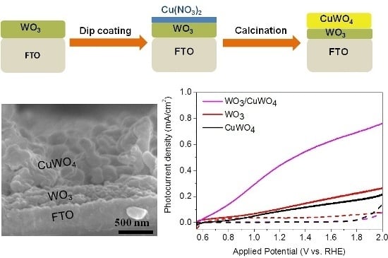
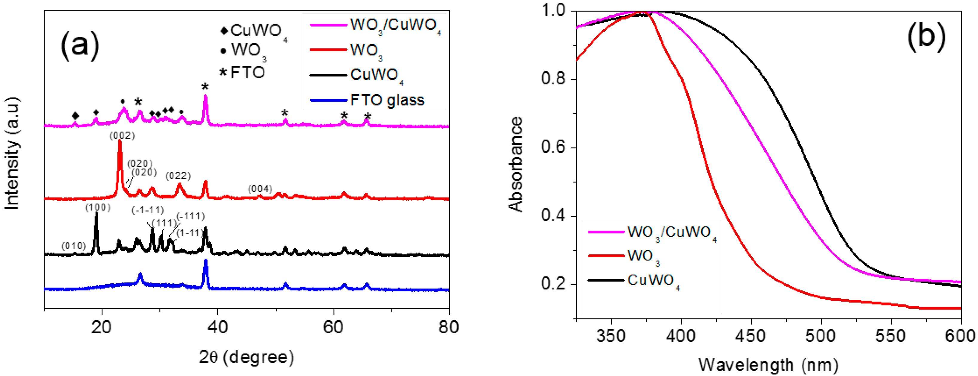
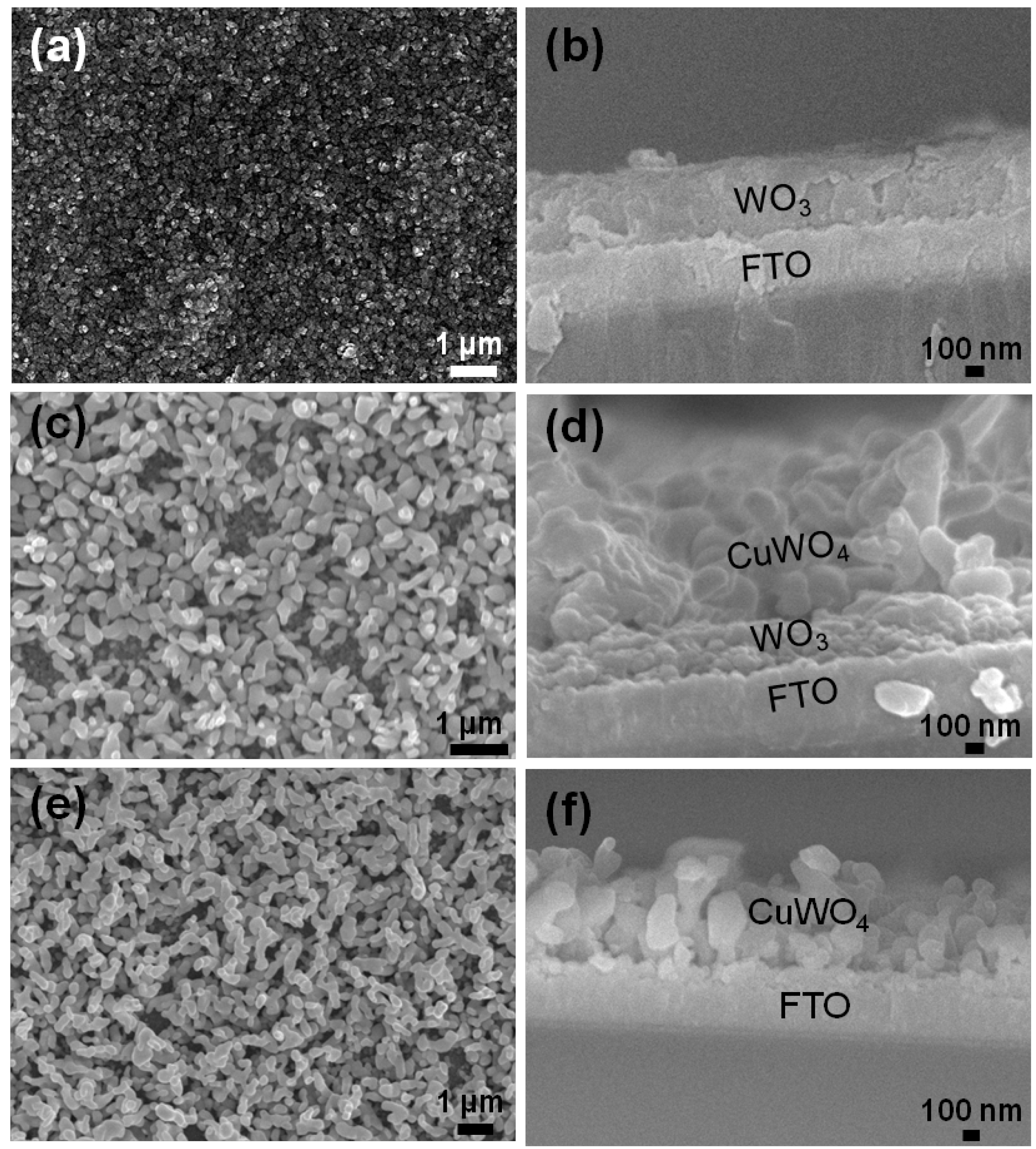
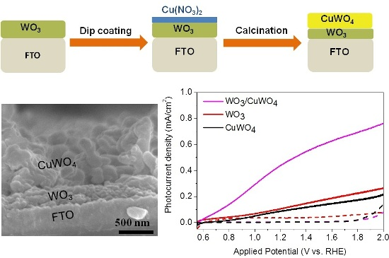
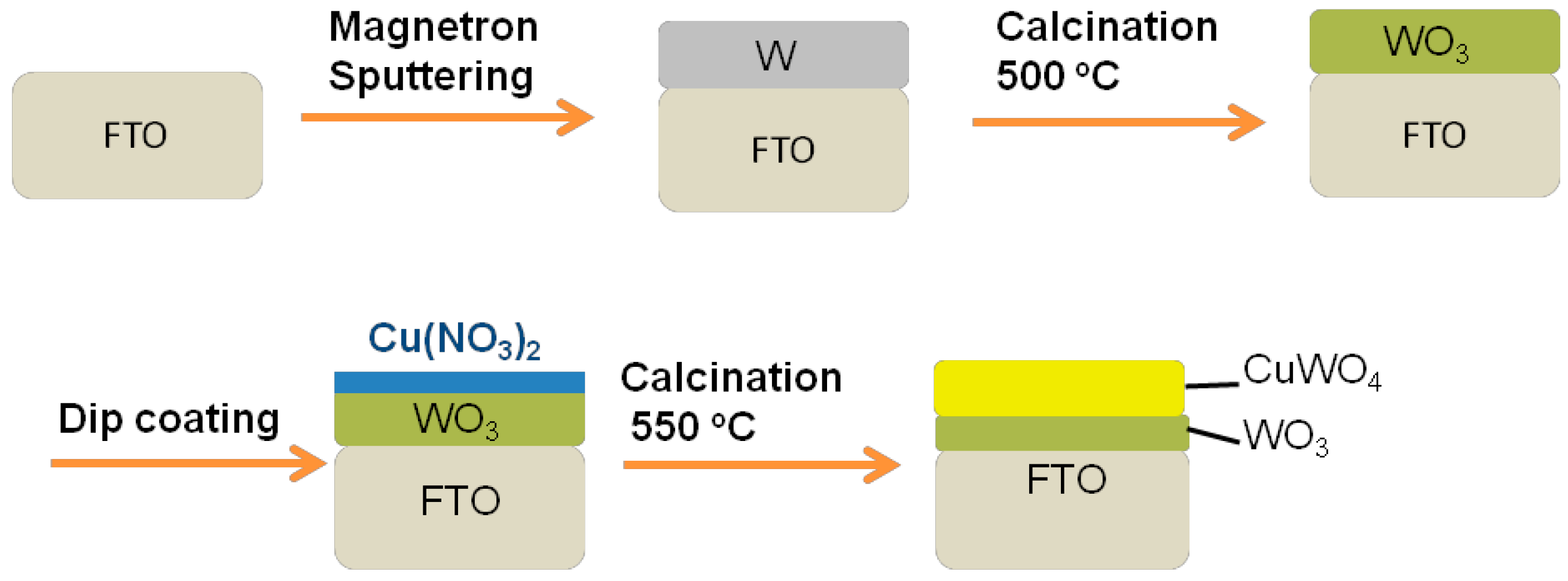
2.1. Synthesis and Characterization of Pristine WO3 and WO3/CuWO4 Composite Thin Films

In this report, three representative samples with 0, 4 and 8 runs of programmed dip coating of Cu2+ solution are discussed, which gave rise to WO3, WO3/CuWO4 composite and CuWO4 materials respectively. XRD patterns in Figure 1 indicate that the WO3 thin films obtained from magnetron sputtered metallic W thin film are of the monoclinic phase (JCPDS No. 43-1035), which is the most photocatalytically active phase for water oxidation [10]. For comparison, we also sputtered metallic W onto a normal glass slide, which produced the orthorhombic phase of WO3 hydrate (JCPDS No. 35-0270) [10], to the contrary, as shown in XRD patterns in Figure S1. It is thus believed that the crystalline layer of F:SnO2 helped with the formation of monoclinic phase of WO3. Thin films of WO3/CuWO4 and CuWO4 showed the characteristic peaks of CuWO4 (JCPDF 72-0616) [9]. UV-Vis/DRS results of the three samples are shown in Figure 1b. Pristine WO3 absorbs light up to 464 nm, which is in accordance with the band gap of about 2.7 eV of monoclinic WO3. The light absorption of CuWO4 extends to 540 nm, corresponding to the smaller band gap of CuWO4 (2.3 eV).
The top and cross-section views of all the films observed by field emission scanning electron microscope (FESEM) are shown in Figure 2. A summary of the average thickness of WO3 and CuWO4 of each sample is provided in Table 1. Figure 2a,b shows the images of pristine WO3. The WO3 thin film was composed of densely assembled WO3 nanoparticles of irregular shape around 50–90 nm in diameter, and the average thickness of film was around 415 nm. Figure 2c,d are the images of WO3/CuWO4 composite thin film, with a porous layer of CuWO4 particles uniformly grown on the WO3 substrate. The thickness of WO3 layer was greatly reduced to 150 nm due to the in situ reaction with Cu2+ ions to form CuWO4. The transmission electron microscope (TEM) image of the scraped particles from the composite film in Figure S2 displays a network-like structure in the thin film, corresponding to the porous CuWO4 nanostructure in FESEM observation. In Figure 2e,f, with further increased loading of Cu2+ ions, the WO3 film was completely consumed, forming a porous layer of CuWO4 1 μm thick.

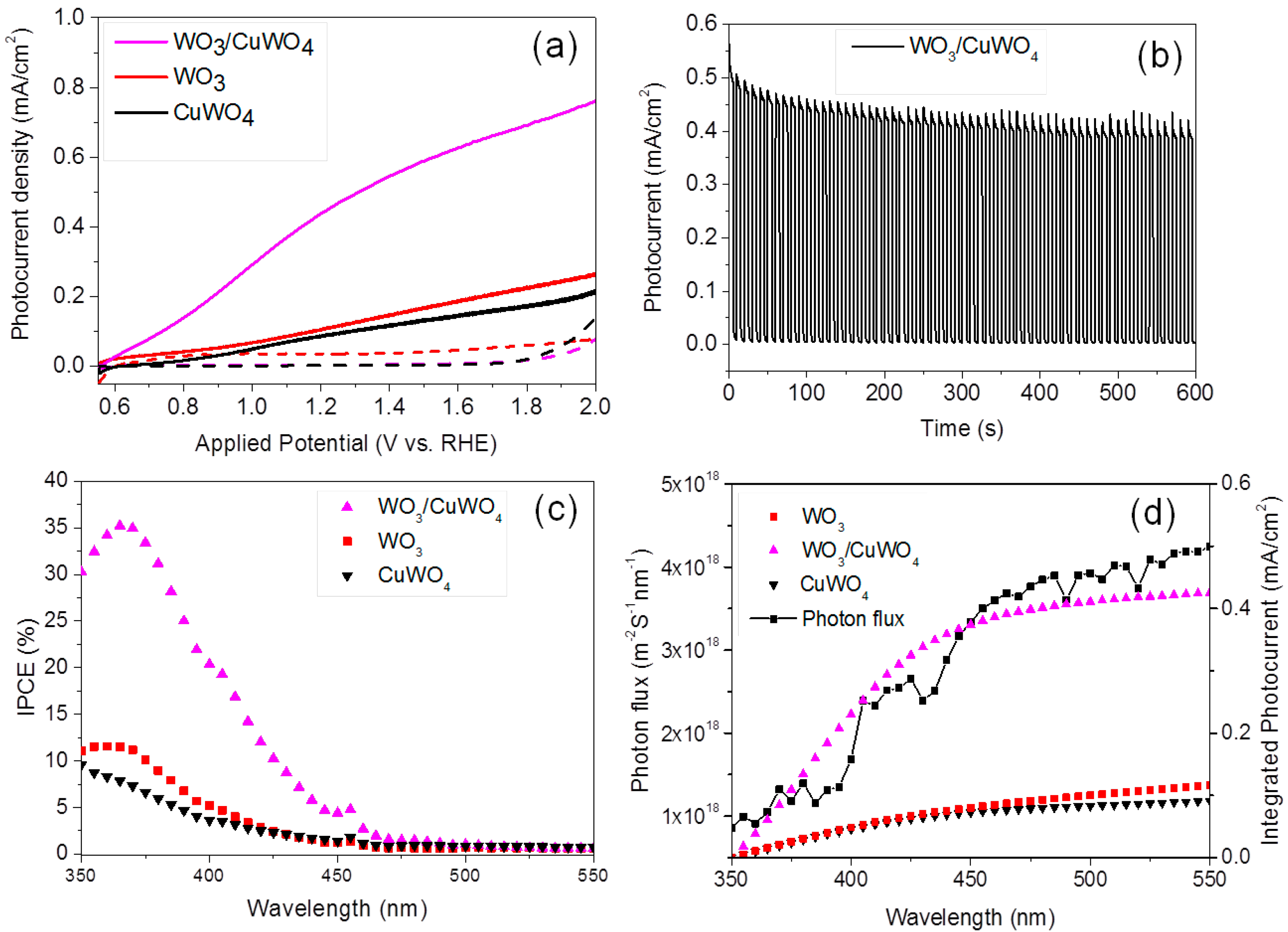
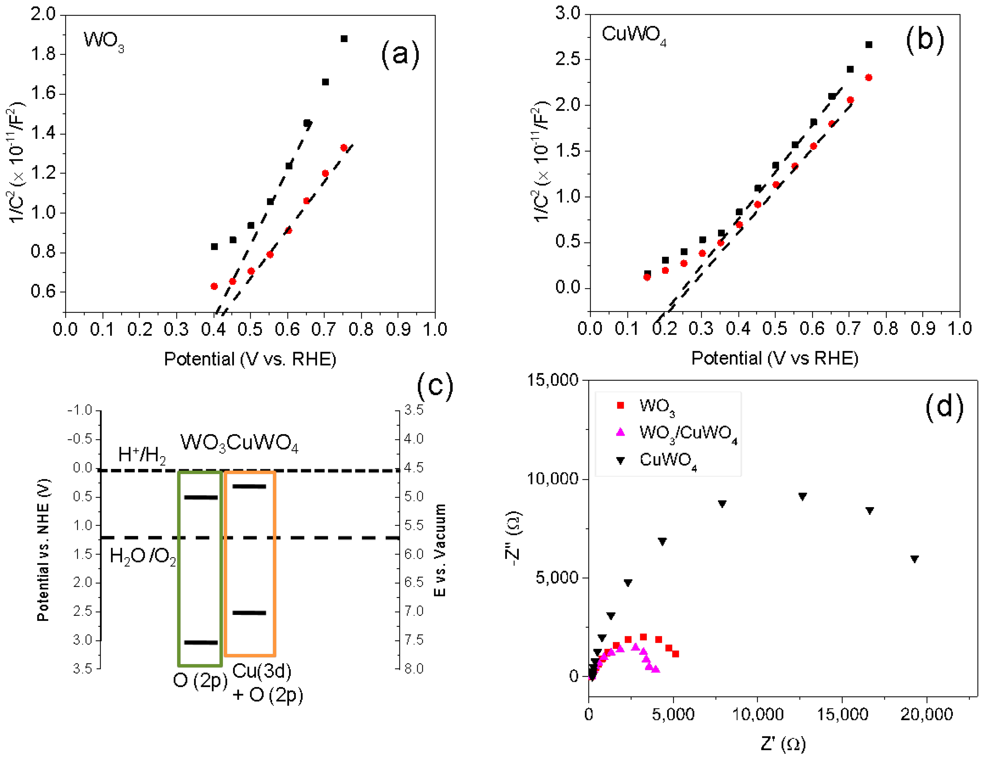
2.2. Photoelectrochemical Performance of Thin Films

The pristine WO3, WO3/CuWO4, and CuWO4 thin films were used as photoanodes in a conventional three-electrode setup. Their PEC performance was investigated by measuring the photocurrent with back-illumination as shown in Figure 3. In the linear sweep voltammetry (LSV) results in Figure 3a, all the samples exhibited negligible photocurrent under dark condition. Composite thin films obtained from different runs are provided in Figure S3. At 1.20 VRHE, bare WO3 and CuWO4 were of very similar photocurrent density, and WO3/CuWO4 (0.45 mA/cm2) showed a current density more than two times higher than WO3 and CuWO4 electrodes. As shown in the supporting information (Figure S3), all the composite thin films demonstrate higher photocurrent compared to single component thin films. The relatively low photocurrent of the WO3 underlayer in our report could be due to the preparation condition and insufficient thickness. As we annealed the tungsten film in air to let it oxidize into WO3, the insertion of oxygen atoms will make the thin film expand. As a result, the back contact with fluorine doped tin oxide (FTO) could be adversely affected. In addition, the annealing temperature and time can also affect the oxygen vacancies and carrier density, which will subsequently influence the photocurrent of WO3 films. However, when a thin layer of WO3 was coupled with CuWO4, the photocurrent of the composite film was remarkably improved compared with the single phase. Figure 3b shows the on-off photocurrent profile of the composite WO3/CuWO4 under a constant bias of 1.20 VRHE, recorded over a duration of 600 s with interval of 5 s. The composite thin film showed a constant photocurrent though transient spikes were spotted for both samples, which could be caused by the surface-trapped photo-generated minority carriers which recombine with the photo-generated major carriers [32]. Figure 3c shows the IPCE curves for WO3, WO3/CuWO4 and CuWO4 electrodes measured at 1.20 VRHE. The WO3/CuWO4 composite thin films had much higher IPCE values compared with WO3 and CuWO4 films. Though light absorption of CuWO4 covered the wavelengths up to 540 nm, the identical wavelength ranges of the three thin films in the IPCE curves indicate that the charge carriers generated in CuWO4 in the wavelength range 470–540 nm make little contribution to photocurrent generation [29,31]. The simulated photocurrents in Figure 3d for all samples were also calculated by integrating the IPCE spectra with a standard AM 1.5 G solar spectrum from Equation (1). The simulated photocurrent is independent of the light source and applied filters, and thus it is more accurate in evaluation of the PEC performance of the thin films. The values obtained were reasonable compared to measured photocurrents.
I simulated = 350 550 ( I P C E ( λ ) × Φ ( λ ) × e ) d λ
where λ is the wavelength of light in unit of nm and IPCE (λ) is measured and calculated as will be described in Experiment Section 3.5. Φ(λ) is the photon flux of sunlight in photons/m2/s. The photon flux can be measured from tabulated solar irradiance data, E(λ), via Φ(λ) = E(λ)/(1240/λ) [33].
In order to measure the band structures of WO3 and CuWO4, the Mott-Schottky measurement is shown in Figure 4a,b, and the result for WO3/CuWO4 composite thin film is shown in Figure S4. Given the band gap measured from UV-Vis absorption, the band structures of WO3 and CuWO4 are shown in Figure 4c. The conduction band of CuWO4 is located at +0.2 eV (vs. normal hydrogen electrode, NHE) and that of WO3 is located at +0.4 eV (vs. NHE), while valence band of CuWO4 is at +2.4 eV (vs. NHE), lower than that of WO3 at +3.0 eV (vs. NHE). Therefore, these two components can form a heterojunction pair, and photo-generated holes from the inner WO3 layer will be transferred to the outer layer of CuWO4 in WO3/CuWO4 composite electrode.
The carrier density can be calculated by
1 C SC 2 = 2 e ε ε 0 N D ( E E fb K b T e )
where CSC, q, ε0, ε, ND, and Efb are capacitance, the electron charge, permittivity in vacuum, dielectric constant, donor carrier density and flat-band potential of the semiconductor, respectively. Using Equation (2), the carrier densities are 1.73 × 10¹⁹ for WO3 and 3.36 × 10¹⁸ for CuWO4. Our low carrier density is possibly due to the synthesis method for the thin films. The literature has shown that annealing in air can affect both the oxygen vacancies and the types of other vacancies/defects within a nanostructured thin film [28].
Electrochemical impedance spectroscopy (EIS) measurements were carried out to evaluate the overall resistance of the three photoanodes, and is shown in Figure 4d under illumination and 1.2 VRHE bias. The semicircle in the medium-frequency region was attributed to the charge-transfer process. The diameter of the WO3/CuWO4 semicircle was the smallest among the three electrodes, which was in accordance with the LSV results [16,25]. CuWO4 had the largest semicircle diameter, indicating a very high charge transfer resistance in the thin film, which was possibly related to the poor intrinsic charge transfer property of CuWO4. However, when CuWO4 was coupled with WO3 to form a heterojunction composite anode, the photogenerated electrons in CuWO4 could be transferred to the WO3 underlayer, with good charge transport characteristics, and contribute to the reduced resistance. Thus, the composite electrode combined the excellent charge transfer characteristics of WO3 and good light absorption capability of CuWO4.

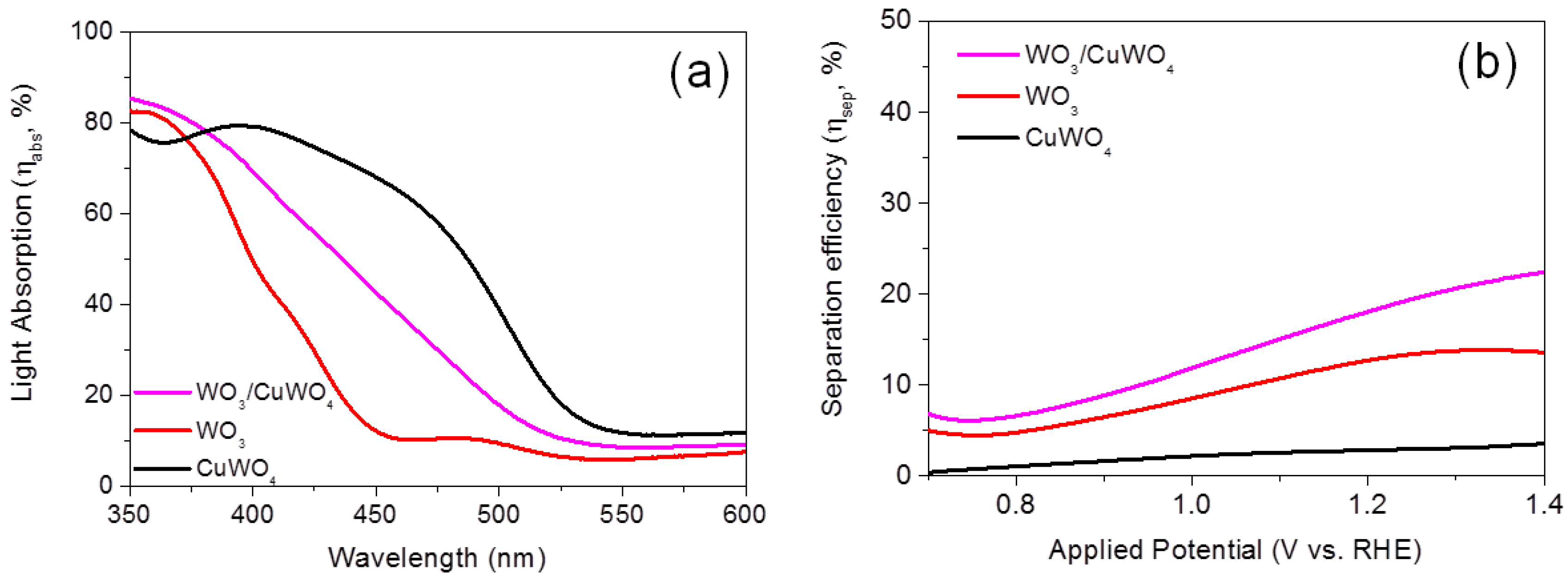
2.3. Comparison of Absorption Efficiency (ηabs), and Charge Separation Efficiency (ηsep) of WO3, CuWO4 and WO3/CuWO4 Thin Films

Since the WO3/CuWO4 electrode demonstrated remarkable improvement in photoelectrochemical and EIS measurement compared with pristine WO3 substrate and CuWO4 films, we further extracted the efficiency values of light absorption (ηabs) and charge separation (ηsep) based on Equations (3) and (4) to quantify the contribution of each factor [34,35].
J a b s = 350 550 ( η a b s   × Φ ( λ ) × e ) d λ
η s e p = J s c a / J a b s
where Jabs is the photo current density calculated by multiplying ηabs by the standard AM 1.5 G (100 mW/cm2) solar spectrum, Φ(λ) is the photon flux of sunlight in photons/m2/s, e is the charge of an electron (C). Jsca is the photocurrent of the photoelectrode in the presence of scavengers as a function of applied bias.
By measuring the light transmittance and reflectance in an integrated sphere (see Figure S5), we were able to obtain the ηabs of pristine WO3, CuWO4 and WO3/CuWO4 in Figure 5a. It shows that more photons can be absorbed in the presence of CuWO4. With the measured values of ηabs and Equation (1), the integrated Jabs over the AM 1.5 spectrum of pristine WO3, CuWO4 and WO3/CuWO4 films are 1.8, 4.7 and 3.2 mA/cm2, respectively. The charge separation efficiency (ηsep) can be determined by adding the hole scavenger H2O2 to the electrolyte. The presence of H2O2 increased photocurrent density of all the three thin films (Figure S6), which was due to the much faster charge transfer rate promoted by the hole scavenger. According to Equation (4), charge separation (ηsep) efficiency of the three films was obtained and shown in Figure 5b. The composite WO3/CuWO4 thin film showed significant improvement of charge separation efficiency compared with CuWO4 film. This indicates that with a thin underlayer of WO3, the charge separation characteristics of CuWO4 are greatly enhanced, which leads to much higher photocurrent.

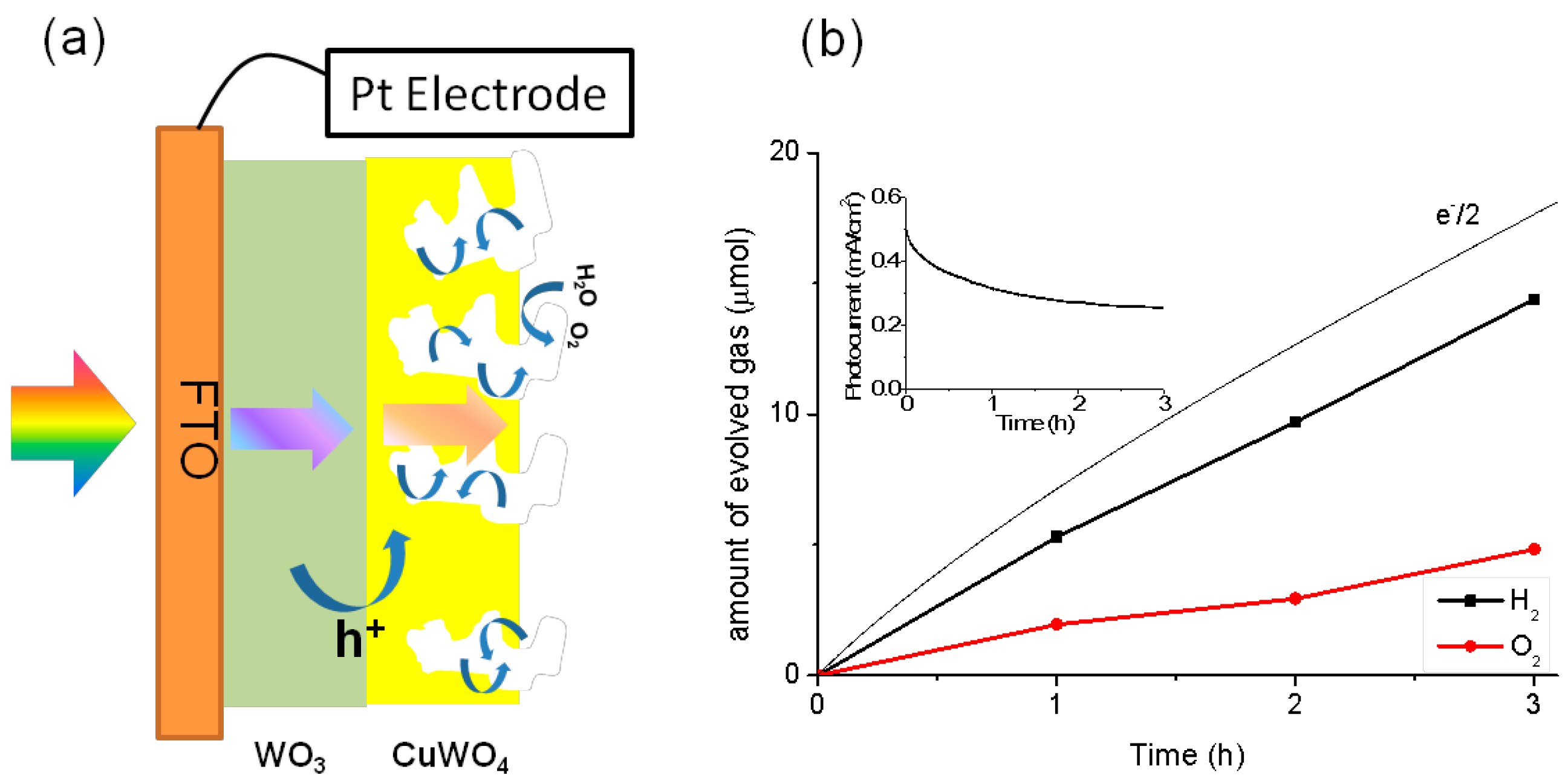
2.4. Photoelectrochemical Water Splitting

In order to confirm that photocurrent was generated by water splitting, we conducted hydrogen and oxygen evolution under AM 1.5 illumination with 1.20 VRHE in 0.5 M Na2SO4 electrolyte. Figure 6a illustrates how the charge carriers are transported in the WO3/CuWO4 composite photoanode. Both WO3 and CuWO4 are excited by back illumination and generate charge carriers. Holes from WO3 are transferred to CuWO4 due to the formation of heterojunction, and are injected into the electrolyte from porous CuWO4 surface to oxidize water into O2. Electrons are directed to the Pt electrode where water molecules are reduced to hydrogen gas. As shown in Figure 6b, the total amount of oxygen and hydrogen evolved in three hours is about 5.0 and 14.0 μmol, respectively. The ratio of H2 to O2 produced is greater than the stoichiometric ratio [36]:
Faradaic Efficiency (FE) % = actual hydrogen evolution rate/calculated amount from photocurrent generation × 100
which was about 79% using the hydrogen quantity calculated according to Equation (5). The loss of faradaic efficiency was possibly due to the slow kinetics of water oxidation and back reaction of H2 and O2. The 3 h time course photocurrent density is presented in the inset of Figure 6b. The photocurrent dropped to around 63% of the initial current density within the first hour, but we believe that the stability of WO3/CuWO4 photoanode could be improved by loading oxygen evolution reaction (OER) co-catalyst on the electrode surface.

3. Materials and Methods

3.1. Preparation of W Thin Film from Magnetron Sputtering

The synthesis route of the WO3/CuWO4 film is shown in Scheme 1. Tungsten film was deposited onto F-doped tin oxide (FTO) glass (sheet resistance ≤ 15 Ω/square, size: 10 mm × 25 mm and thickness: 2.2 mm) using direct current (DC) magnetron sputtering. The FTO glass was cleaned using acetone, ethanol and DI water prior to the sputtering. A metallic tungsten target (W, 3.00′′ diameter × 0.250′′ thick, 99.95% purity, Kurt J. Lesker, Jefferson Hills, PA, USA) was used as the sputtering target. The distance between the target and the substrate was set at around 10 cm. The sputtering chamber was evacuated to 8.0 × 10⁻⁶ Torr or lower using a rotary pump and a turbo pump before introducing argon gas. The argon flow rate was kept constant at 20 sccm. A manual gate valve was used to fix the pressure inside the sputtering chamber at 20.0 mTorr during film deposition. The surface of the target was cleaned by sputtering the W target for 10 min before deposition onto FTO glass. The whole sputtering process lasted for 5.0 min at a constant working power of 230 W to obtain the black metallic W thin film.

3.2. Fabrication of WO3 Thin Film

The as-prepared metallic W thin film was placed in a clean porcelain crucible, and was transferred to a muffle furnace (CWF 12/5, Carbolite, Derbyshire, UK). The thin film was calcined at 500 °C for 2 h with a ramping rate of 2 °C/min for heating step and was cooled down naturally. Monoclinic WO3 thin film with a light yellow colour was obtained.

3.3. Fabrication of WO3/CuWO4 Thin Films

0.2 M of copper nitrate trihydrate (Cu(NO3)2∙3H2O, Sigma-Aldrich, St. Louis, MO, USA) ethanol solution with 0.04 g/mL of Pluronic® F-127 (Sigma-Aldrich, St. Louis, MO, USA) was prepared as the dip coating solution. The FTO/WO3 was installed on dip coater (KSV NIMA), with insertion and withdrawal speed of 100 mm/min and 30 s submerge duration in Cu(NO3)2∙3H2O ethanol solution. The process was repeated for 4 and 8 runs to load different amount of Cu2+ ions. The films were subsequently heated in air at 550 C for 4 h in a muffle furnace, with a ramping rate of 2 °C/min for both heating and cooling steps. After annealing, the colour of the thin film changed to bright yellow, indicating the formation of a layer of CuWO4 during heat treatment. CuO that formed from decomposition of excess Cu(NO3)2 along the edges of WO3 thin film and FTO glass during heating was dissolved away by soaking in a 0.5 M HCl solution for 10 min.

3.4. Material Characterization

X-ray diffraction (XRD) patterns of all the thin films were recorded using XRD-6000 X-ray diffractometer (Shimadzu, Kyoto, Japan) with Cu Kα radiation (λ = 0.15418 nm). The surface morphology was analyzed by FESEM (JSM-7600F, JEOL, Tokyo, Japan). The morphology of CuWO4 nanoparticles were observed using TEM (JEM-2010, JEOL, Tokyo, Japan).UV-Vis/DRS of thin films was recorded using a Varian Cary 5000 UV-Vis spectrophotometer (Varian/Agilent, Santa Clara, CA, USA), with BaSO4 as a reference. Absorption efficiency (ηabs) of thin films was determined by measuring transmission and reflection spectra using integrating sphere (Absorbance = 1 − Transmittance − Reflectance) [37].

3.5. Photoelectrochemical (PEC) Measurement

To investigate the photoelectrochemical properties of WO3, WO3/CuWO4, and CuWO4 photoanodes, a conventional three-electrode system was used. All the PEC measurements were carried out in a home-made Teflon PEC cell with an illumination window of 5 mm inner diameter for back-illumination. The surface area of electrode exposed under illumination was about 0.2 cm2. 0.5 M of sodium sulphate (Na2SO4, Sigma-Aldrich, St. Louis, MO, USA) in deionized water solution with a pH value of 6 was used as the electrolyte. Platinum (Pt) coil and silver/silver chloride (Ag/AgCl) were used as counter and reference electrodes, respectively. The prepared thin films were used as working electrodes. The light source was simulated sunlight from a 150 W xenon solar simulator (67005, Newport Corp., Irvine, CA, USA) through an Air Mass filter (AM 1.5, Global, 81094, Newport Corp., Irvine, CA, USA) with a constant light intensity to standard AM1.5 sunlight (100 mW/cm2) at the photoanode surface. Linear sweep voltammetry (LSV) was carried out by an electrochemistry workstation (CHI 852C, CH Instruments, Shanghai, China) both in dark and under AM1.5 sunlight simulator. Stability of WO3/CuWO4 sample was carried out at a bias potential of 1.20 VRHE for 600 s with illumination on-off interval of 5 s. Charge separation efficiency was obtained by measuring light absorption of thin films and photocurrent in 0.5 M Na2SO4 + 0.5 M H2O2 aqueous solution. Incident photon to electron conversion efficiency (IPCE) was measured with a xenon light source (66983, Newport Corp., Irvine, CA, USA) coupled with a monochromator (74125, Newport Corp., Irvine, CA, USA) at a bias of 1.20 VRHE from back illumination. A Si photodiode (DH-Si, Bentham, Reading, Berkshire, UK) with known IPCE was used to calculate the IPCE of prepared thin films. A source meter (Keithley Instruments Inc., Solon, OH, USA, Model: 2400) was used to record the photocurrent of Si diode. CHI 852C electrochemistry workstation was used to record the photocurrent of each photoanode. IPCE calculation is given in the following formula:
IPCE (λ) = 100 × 1240 × (J(λ) − Jdark)/λ/I(λ) [38]
where λ is the wavelength of light in unit of nm; J(λ) is the photocurrent density in mA/cm2 under illumination at λ; Jdark is the photocurrent density measured at dark; and I(λ) is the incident light intensity in mW/cm2 at λ [38].
Electrochemical impedance spectroscopy (EIS) was performed using an Autolab PGSTAT 302N system (Metrohm Autolab, Utrecht, The Netherlands) equipped with the FAR2 Faraday impedance module (Metrohm Autolab, Utrecht, The Netherlands). The flat band potential of CuWO4 was determined using the Mott-Schottky equation on a CuWO4 sample at frequencies of 5 k and 10 k Hz. The Nyquist plot was measured at 1.20 VRHE with a frequency ranging from 0.01 Hz to 100 kHz at 10 mV amplitude potential under AM1.5 illumination.

3.6. Photoelectrochemical Water Splitting

The photoelectrochemical water splitting was carried out in an air-tight reactor using back illumination. The light source (AM 1.5 sunlight, 100 mW/cm2) and applied bias 1.20 VRHE were kept the same during the measurement. The amount of hydrogen and oxygen was analyzed by a gas chromatographer (GC-7890A, Agilent, Agilent, Santa Clara, CA, USA) equipped with thermal conductivity detector (TCD) detector.

4. Conclusions

In conclusion, we have converted monoclinic WO3 thin film into WO3/CuWO4 composite and CuWO4 films through a facile dip-coating step followed by heat treatment. The PEC and EIS measurements showed that the presence of a thin layer of WO3 beneath CuWO4 can enhance the photocurrent density and reduce the charge transfer resistance compared with pure CuWO4 film. By separately studying the photo absorption and charge transfer efficiencies, it was demonstrated that the WO3/CuWO4 composite film exhibited enhancements in each process compared with single-phase WO3 and CuWO4. Hydrogen and oxygen evolution was conducted to confirm that the photocurrent was generated from water splitting. Our result has provided a low-cost and controllable method to prepare WO3-metal tungstate heterojunction thin films, and helped to provide a reference for designing CuWO4-based photoanodes with greater efficiency.

Supplementary Materials

The following are available online at www.mdpi.com/1996-1944/9/5/348/s1. Figure S1: XRD patterns of different WO3 phases obtained from magnetron sputtering on FTO (red) and normal glass slide (blue) substrates, which showed the FTO layer helped to induce the crystal growth of monoclinic WO3. Figure S2: TEM images of particles scraped from WO3/CuWO4, indicating network morphology of the CuWO4 layer. Figure S3: Photocurrent comparison of thin film obtained from different runs of dip coating. Figure S4: Mott-Schottky plots of WO3/CuWO4 thin film at 10 k and 5 k Hz under dark conditions. Figure S5: Absorption efficiency of the WO3, CuWO4 and WO3/CuWO4 thin film by measuring the transmission and reflection spectra using an integrating sphere (Absorbance (ηabs) = 1 − Transmittance − Reflectance). Figure S6: Linear sweep voltammetry of all samples with (solid lines) and without the illumination of AM 1.5 (dashed lines), measured in 0.5 M Na2SO4 + 0.5 M H2O2 aqueous solution.

Acknowledgments

This research project is funded by the National Research Foundation (NRF), Prime Minister’s Office, Singapore under its Campus for Research Excellence and Technological Enterprise (CREATE) program.

Author Contributions

Danping Wang, Lydia Helena Wong and Zhong Chen primarily designed the experiments. Danping Wang, Prince Saurabh Bassi, Huan Qi, Xin Zhao and Gurudayal carried out the experiments and material characterizations. Danping Wang, Prince Saurabh Bassi, Xin Zhao and Gurudayal analyzed the experiment results. Danping Wang wrote the manuscript with the input from Zhong Chen, Lydia Helena Wong, Rong Xu and Thirumany Sritharan.

Conflicts of Interest

The authors declare no conflict of interest.

References

  1. Gust, D.; Moore, T.A.; Moore, A.L. Solar fuels via artificial photosynthesis. Acc. Chem. Res. 2009, 42, 1890–1898. [Google Scholar] [CrossRef] [PubMed]
  2. Sivula, K.; Le Formal, F.; Gratzel, M. Solar water splitting: Progress using hematite (alpha-Fe2O3) photoelectrodes. Chemsuschem 2011, 4, 432–449. [Google Scholar] [CrossRef] [PubMed]
  3. Walter, M.G.; Warren, E.L.; McKone, J.R.; Boettcher, S.W.; Mi, Q.X.; Santori, E.A.; Lewis, N.S. Solar water splitting cells. Chem. Rev. 2010, 110, 6446–6473. [Google Scholar] [CrossRef] [PubMed]
  4. Youngblood, W.J.; Lee, S.-H.A.; Kobayashi, Y.; Hernandez-Pagan, E.A.; Hoertz, P.G.; Moore, T.A.; Moore, A.L.; Gust, D.; Mallouk, T.E. Photoassisted overall water splitting in a visible light-absorbing dye-sensitized photoelectrochemical cell. J. Am. Chem. Soc. 2009, 131, 926–927. [Google Scholar] [CrossRef] [PubMed]
  5. Dareedwards, M.P.; Goodenough, J.B.; Hamnett, A.; Trevellick, P.R. Electrochemistry and photoelectrochemistry of iron(III) oxide. J. Chem. Soc. Faraday Trans. I 1983, 79, 2027–2041. [Google Scholar] [CrossRef]
  6. Kennedy, J.H.; Frese, K.W. Photo-oxidation of water at alpha-Fe2O3 electrodes. J. Electrochem. Soc. 1978, 125, 709–714. [Google Scholar] [CrossRef]
  7. Gardner, R.F.G.; Tanner, D.W.; Sweett, F. Electrical properties of alpha ferric oxide. 2. Ferric oxide of high purity. J. Phys. Chem. Solids 1963, 24, 1183–1196. [Google Scholar] [CrossRef]
  8. Butler, M.A. Photoelectrolysis and physical-properties of semiconducting electrode WO3. J. Appl. Phys. 1977, 48, 1914–1920. [Google Scholar] [CrossRef]
  9. Yourey, J.E.; Bartlett, B.M. Electrochemical deposition and photoelectrochemistry of CuWO4, a promising photoanode for water oxidation. J. Mater. Chem. 2011, 21, 7651–7660. [Google Scholar] [CrossRef]
  10. Kalanur, S.S.; Hwang, Y.J.; Chae, S.Y.; Joo, O.S. Facile growth of aligned WO3 nanorods on FTO substrate for enhanced photoanodic water oxidation activity. J. Mater. Chem. A 2013, 1, 3479–3488. [Google Scholar] [CrossRef]
  11. Waller, M.R.; Townsend, T.K.; Zhao, J.; Sabio, E.M.; Chamousis, R.L.; Browning, N.D.; Osterloh, F.E. Single-crystal tungsten oxide nanosheets: Photochemical water oxidation in the quantum confinement regime. Chem. Mater. 2012, 24, 698–704. [Google Scholar] [CrossRef]
  12. Su, J.Z.; Feng, X.J.; Sloppy, J.D.; Guo, L.J.; Grimes, C.A. Vertically aligned WO3 nanowire arrays grown directly on transparent conducting oxide coated glass: Synthesis and photoelectrochemical properties. Nano Lett. 2011, 11, 203–208. [Google Scholar] [CrossRef] [PubMed]
  13. Zheng, J.Y.; Song, G.; Kim, C.W.; Kang, Y.S. Facile preparation of p-CuO and p-CuO/n-CuWO4 junction thin films and their photoelectrochemical properties. Electrochim. Acta 2012, 69, 340–344. [Google Scholar] [CrossRef]
  14. Yourey, J.E.; Pyper, K.J.; Kurtz, J.B.; Bartlett, B.M. Chemical stability of CuWO4 for photoelectrochemical water oxidation. J. Phys. Chem. C 2013, 117, 8708–8718. [Google Scholar] [CrossRef]
  15. Yourey, J.E.; Kurtz, J.B.; Bartlett, B.M. Water oxidation on a CuWO4-WO3 composite electrode in the presence of [Fe(CN)6]3−: Toward solar z-scheme water splitting at zero bias. J. Phys. Chem. C 2012, 116, 3200–3205. [Google Scholar] [CrossRef]
  16. Pilli, S.K.; Deutsch, T.G.; Furtak, T.E.; Brown, L.D.; Turner, J.A.; Herring, A.M. BiVO4/CuWO4 heterojunction photoanodes for efficient solar driven water oxidation. Phys. Chem. Chem. Phys. 2013, 15, 3273–3278. [Google Scholar] [CrossRef] [PubMed]
  17. Pandey, P.K.; Bhave, N.S.; Kharat, R.B. Spray deposition process of polycrystalline thin films of CuWO4 and study on its photovoltaic electrochemical properties. Mater. Lett. 2005, 59, 3149–3155. [Google Scholar] [CrossRef]
  18. Gaillard, N.; Chang, Y.C.; DeAngelis, A.; Higgins, S.; Braun, A. A nanocomposite photoelectrode made of 2.2 ev band gap copper tungstate (CuWO4) and multi-wall carbon nanotubes for solar-assisted water splitting. Int. J. Hydrog. Energy 2013, 38, 3166–3176. [Google Scholar] [CrossRef]
  19. Benko, F.A.; Maclaurin, C.L.; Koffyberg, F.P. CuWO4 and Cu3WO6 as anodes for the photoelectrolysis of water. Mater. Res. Bull. 1982, 17, 133–136. [Google Scholar] [CrossRef]
  20. Hill, J.C.; Choi, K.S. Synthesis and characterization of high surface area CuWO4 and Bi2WO6 electrodes for use as photoanodes for solar water oxidation. J. Mater. Chem. A 2013, 1, 5006–5014. [Google Scholar] [CrossRef]
  21. Koo, H.J.; Whangbo, M.H. Spin dimer analysis of the anisotropic spin exchange interactions in the distorted wolframite-type oxides CuWO4, CuMoO4-III, and Cu(Mo0.25W0.75)O4. Inorg. Chem. 2001, 40, 2161–2169. [Google Scholar] [CrossRef] [PubMed]
  22. Montini, T.; Gombac, V.; Hameed, A.; Felisari, L.; Adami, G.; Fornasiero, P. Synthesis, characterization and photocatalytic performance of transition metal tungstates. Chem. Phys. Lett. 2010, 498, 113–119. [Google Scholar] [CrossRef]
  23. Lalic, M.V.; Popovic, Z.S.; Vukajlovic, F.R. Electronic structure and optical properties of CuWO4: An ab initio study. Comput. Mater. Sci. 2012, 63, 163–167. [Google Scholar] [CrossRef]
  24. Lalic, M.V.; Popovic, Z.S.; Vukajlovic, F.R. Ab initio study of electronic, magnetic and optical properties of CuWO4 tungstate. Comput. Mater. Sci. 2011, 50, 1179–1186. [Google Scholar] [CrossRef]
  25. Chang, Y.C.; Braun, A.; Deangelis, A.; Kaneshiro, J.; Gaillard, N. Effect of thermal treatment on the crystallographic, surface energetics, and photoelectrochemical properties of reactively cosputtered copper tungstate for water splitting. J. Phys. Chem. C 2011, 115, 25490–25495. [Google Scholar] [CrossRef]
  26. Hill, J.C.; Ping, Y.; Galli, G.A.; Choi, K.S. Synthesis, photoelectrochemical properties, and first principles study of n-type CuW1-xMoxO4 electrodes showing enhanced visible light absorption. Energy Environ. Sci. 2013, 6, 2440–2446. [Google Scholar] [CrossRef]
  27. Valenti, M.; Dolat, D.; Biskos, G.; Schmidt-Ott, A.; Smith, W.A. Enhancement of the photoelectrochemical performance of CuWO4 thin films for solar water splitting by plasmonic nanoparticle functionalization. J. Phys. Chem. C 2015, 119, 2096–2104. [Google Scholar] [CrossRef]
  28. Zhang, H.; Yilmaz, P.; Ansari, J.O.; Khan, F.F.; Binions, R.; Krause, S.; Dunn, S. Incorporation of Ag nanowires in CuWO4 for improved visible light-induced photoanode performance. J. Mater. Chem. A 2015, 3, 9638–9644. [Google Scholar] [CrossRef]
  29. Nam, K.M.; Cheon, E.A.; Shin, W.J.; Bard, A.J. Improved photoelectrochemical water oxidation by the WO3/CuWO4 composite with a manganese phosphate electrocatalyst. Langmuir 2015, 31, 10897–10903. [Google Scholar] [CrossRef] [PubMed]
  30. Gao, Y.; Zandi, O.; Hamann, T.W. Atomic layer stack deposition-annealing synthesis of CuWO4. J. Mater. Chem. A 2016, 4, 2826–2830. [Google Scholar] [CrossRef]
  31. Zhan, F.; Li, J.; Li, W.; Liu, Y.; Xie, R.; Yang, Y.; Li, Y.; Chen, Q. In situ formation of CuWO4/WO3 heterojunction plates array films with enhanced photoelectrochemical properties. Int. J. Hydrog. Energy 2015, 40, 6512–6520. [Google Scholar] [CrossRef]
  32. Jiang, Z.; Tang, Y.; Tay, Q.; Zhang, Y.; Malyi, O.I.; Wang, D.; Deng, J.; Lai, Y.; Zhou, H.; Chen, X.; et al. Understanding the role of nanostructures for efficient hydrogen generation on immobilized photocatalysts. Adv. Energy Mater. 2013, 3, 1368–1380. [Google Scholar] [CrossRef]
  33. Van de Krol, R.; Gratzel, M. (Eds.) Photoelectrochemical Hydrogen Production; Springer: New York, NY, USA, 2012; p. 54.
  34. Li, Z.; Feng, J.; Yan, S.; Zou, Z. Solar fuel production: Strategies and new opportunities with nanostructures. Nano Today 2015, 10, 468–486. [Google Scholar] [CrossRef]
  35. Dotan, H.; Sivula, K.; Gratzel, M.; Rothschild, A.; Warren, S.C. Probing the photoelectrochemical properties of hematite (α-Fe2O3) electrodes using hydrogen peroxide as a hole scavenger. Energy Environ. Sci. 2011, 4, 958–964. [Google Scholar] [CrossRef]
  36. Kim, E.S.; Kang, H.J.; Magesh, G.; Kim, J.Y.; Jang, J.-W.; Lee, J.S. Improved photoelectrochemical activity of CaFe2O4/BiVO4 heterojunction photoanode by reduced surface recombination in solar water oxidation. ACS Appl. Mater. Interfaces 2014, 6, 17762–17769. [Google Scholar] [CrossRef] [PubMed]
  37. Zhao, X.; Luo, W.; Feng, J.; Li, M.; Li, Z.; Yu, T.; Zou, Z. Quantitative analysis and visualized evidence for high charge separation efficiency in a solid-liquid bulk heterojunction. Adv. Energy Mater. 2014, 4. [Google Scholar] [CrossRef]
  38. Lin, J.D.; Hu, P.; Zhang, Y.; Fan, M.T.; He, Z.M.; Ngaw, C.K.; Loo, J.S.C.; Liao, D.W.; Tan, T.T.Y. Understanding the photoelectrochemical properties of a reduced graphene oxide-WO3 heterojunction photoanode for efficient solar-light-driven overall water splitting. RSC Adv. 2013, 3, 9330–9336. [Google Scholar] [CrossRef]
Figure 1. XRD patterns (a) and UV-Vis absorption spectrum (b) of pristine WO3, WO3/CuWO4, and CuWO4 thin films.
Materials 09 00348 g001
Figure 2. FESEM images of top and cross-section views of WO3 (a,b); WO3/CuWO4 composite (c,d) and CuWO4 (e,f) thin films.
Materials 09 00348 g002
Figure 3. (a) Linear sweep voltammetry of WO3, WO3/CuWO4 and CuWO4 electrodes (solid lines: photocurrent under AM 1.5G illumination, dashed lines: dark current); (b) Photocurrent stability of WO3/CuWO4 electrode at 600 s; (c) IPCE measurement of WO3, WO3/CuWO4, and CuWO4 electrodes (note: IPCE was done using back illumination which is in accordance with photocurrent-potential measurement); (d) Integrated photocurrent based on the IPCE data (350–550 nm), solar photon flux is shown as a reference. (ac) were tested in 0.5 M of Na2SO4 aqueous solution with illumination of AM 1.5; and (b,c) had 1.20 VRHE bias applied to the electrodes.
Materials 09 00348 g003
Figure 4. Mott-Schottky plots of WO3 thin film (a); and CuWO4 thin film (b) at 10 k and 5 k Hz under dark conditions; (c) Band structure of WO3 and CuWO4; (d) Nyquist plots of WO3, WO3/CuWO4, and CuWO4 thin films under AM 1.5 illumination in 0.5 M Na2SO4 with 1.20 VRHE applied bias.
Materials 09 00348 g004
Figure 5. (a) Light absorption efficiency of WO3, CuWO4 and WO3/CuWO4 films obtained from an integrating sphere; (b) Charge separation efficiency of WO3, CuWO4 and WO3/CuWO4 electrodes.
Materials 09 00348 g005
Figure 6. (a) Illustration of working mechanism of WO3/CuWO4 composite photoanode; and (b) hydrogen and oxygen evolution by WO3/CuWO4 photoanode under AM 1.5 illumination in 0.5 M Na2SO4 at bias of 1.20 VRHE. The expected amount of hydrogen gas, e/2 is also provided for evaluation of Faradaic efficiency. Inset graph shows the time course of photocurrent generation in 3 h.
Materials 09 00348 g006
Scheme 1. Preparation of FTO/W, FTO/WO3, FTO/WO3/Cu2+ and FTO/WO3/CuWO4 thin films.
Materials 09 00348 sch001
Table 1. Summary of the thickness of the WO3 and CuWO4 layers of the three samples.
SampleThickness of WO3 (nm)Thickness of CuWO4 (nm)
Pristine WO34150
WO3/CuWO4150600
CuWO401000

