
Influence of Oxygen Concentration on the Performance of Ultra-Thin RF Magnetron Sputter Deposited Indium Tin Oxide Films as a Top Electrode for Photovoltaic Devices

 ,
, 
Abstract
:1. Introduction
2. Materials and Methods
2.1. ITO Fabrication Process
2.2. Chemical Shaving: Wet Etching
3. Results
3.1. Structural Analysis
3.1.1. XRD Analysis


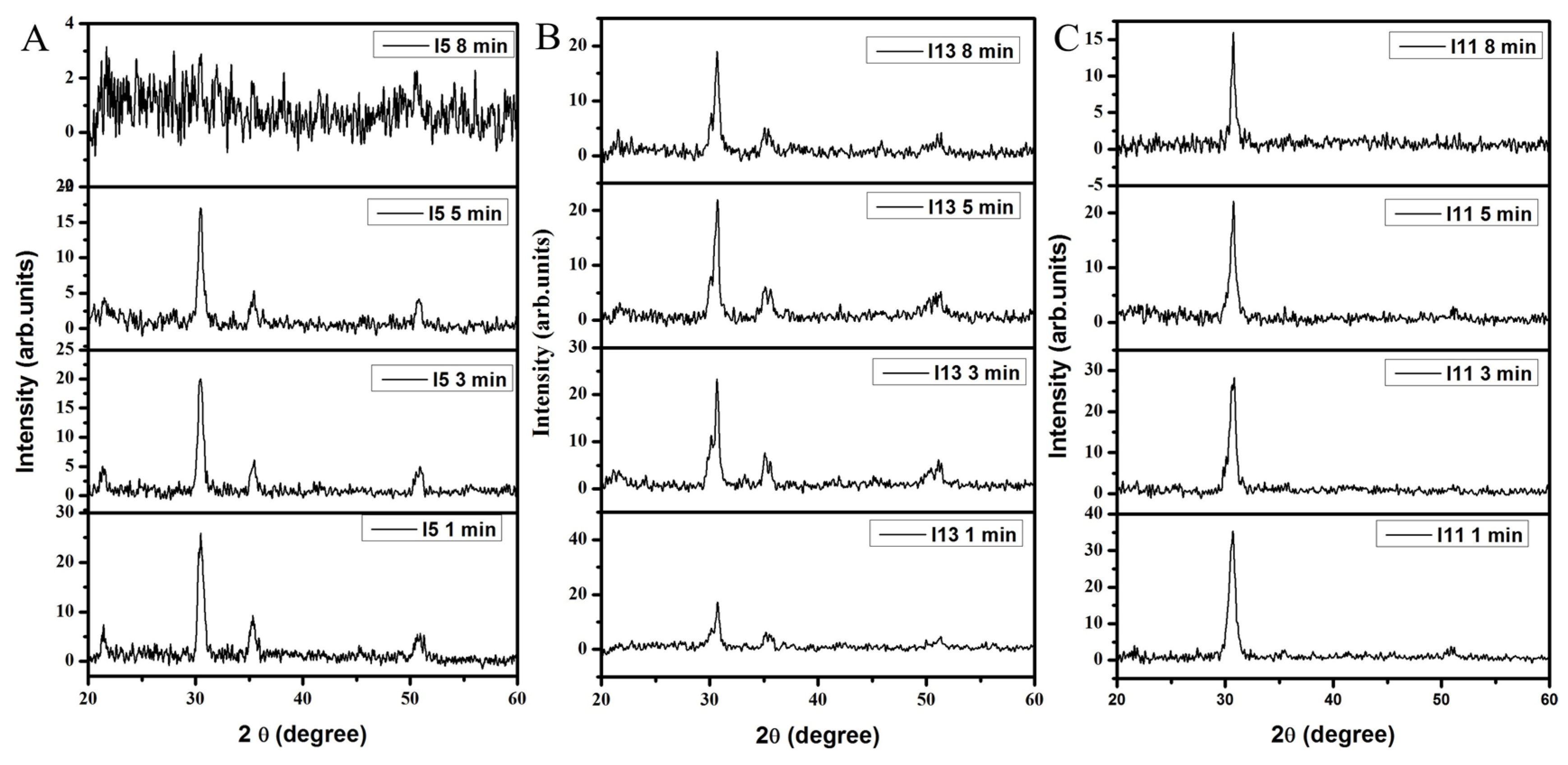
| Oxygen Flow Rate (sccm) | Etching Time (min) | D Spacing (222) (Å) | Lattice Constant (222) (Å) | Net-Lattice Distortion | Grain Size (222) (nm) |
|---|---|---|---|---|---|
| Standard JCPDS for ITO 06-0416 | – | 2.921 | 10.1180 | – | – |
| 0 | 1 | 2.932 | 10.1552 | –0.0036 | 16 |
| 3 | 2.934 | 10.1629 | –0.2970 | 16 | |
| 5 | 2.934 | 10.1629 | –0.2885 | 17 | |
| 8 | – | – | – | – | |
| 0.4 | 1 | 2.908 | 10.0731 | –0.0075 | 31 |
| 3 | 2.912 | 10.0869 | –0.0157 | 25 | |
| 5 | 2.914 | 10.0954 | –0.0153 | 23 | |
| 8 | 2.914 | 10.0954 | –0.0169 | 20 | |
| 1.0 | 1 | 2.917 | 10.1059 | – | 13 |
| 3 | 2.913 | 10.0915 | –0.2828 | 13 | |
| 5 | 2.911 | 10.0845 | – | 14 | |
| 8 | 2.908 | 10.0764 | – | 19 |
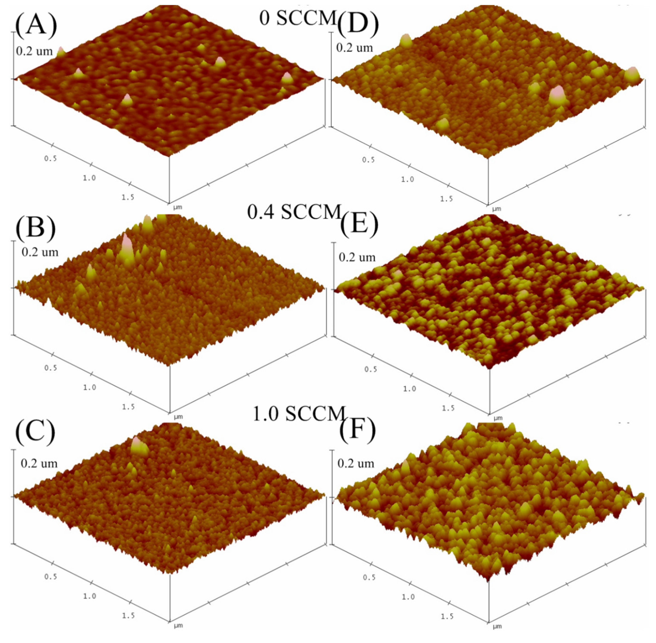
3.1.2. AFM Analysis
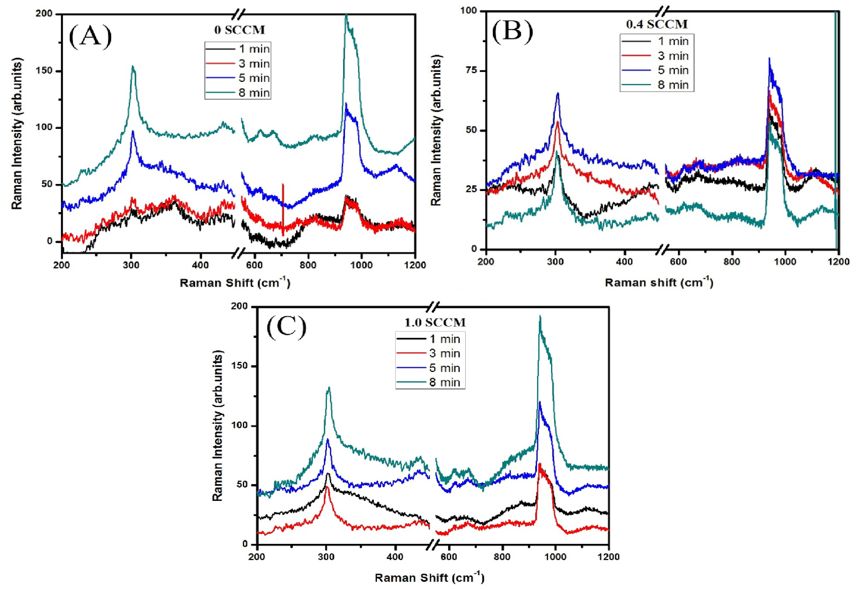
3.1.3. Raman Spectroscopy

3.2. Resistivity
| Oxygen Flow Rate (sccm) | Etching Time (min) | Sheet Resistance (Ω/square) | Thickness (nm) | Resistivity (Ω·cm) | Transmission (%) |
|---|---|---|---|---|---|
| 0 | 1 | 83.28 | 70 | 5.83 × 10⁻⁴ | 76.29 |
| 3 | 103.47 | 59 | 6.11 × 10⁻⁴ | 93.98 | |
| 5 | 209.49 | 44 | 9.22 × 10⁻⁴ | 90.27 | |
| 8 | – | – | – | 100 | |
| 0.4 | 1 | 209.02 | 89 | 1.86 × 10⁻³ | 91.45 |
| 3 | 194.23 | 88 | 1.71 × 10⁻³ | 85.26 | |
| 5 | 240.08 | 85 | 2.04 × 10⁻³ | 84.85 | |
| 8 | 326.9 | 47 | 1.54 × 10⁻³ | 83.71 | |
| 1.0 | 1 | 1000 | 84 | 8.4 × 10⁻³ | 90.96 |
| 3 | 2000 | 62 | 1.24 × 10⁻² | 89.25 | |
| 5 | 2400 | 50 | 1.20 × 10⁻² | 100 | |
| 8 | 7350 | 22 | 1.62 × 10⁻² | 100 |
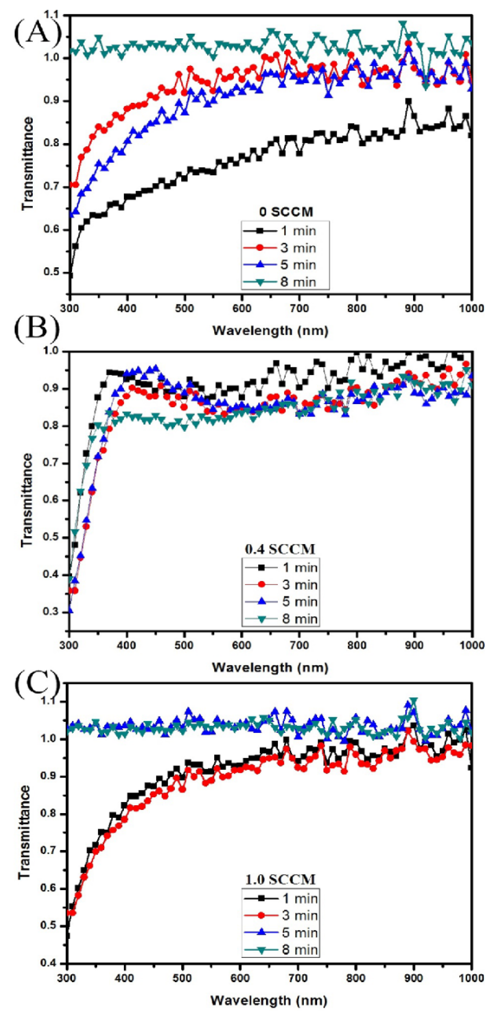
3.3. Transmittance
4. Discussion
5. Conclusions
Acknowledgments
Author Contributions
Conflicts of Interest
Abbreviations
| 4-PP | Four Point Probe |
| AFM | Atomic Force Microscopy |
| a-Si:H | Hydrogenated Amorphous Silicon |
| AZO | Aluminum doped Zinc Oxide |
| c-Si | Crystalline Silicon |
| DC | Direct Current |
| FTO | Fluorine doped-Tin oxide |
| ITO | Indium Tin Oxide |
| PV | Photovoltaic |
| RF | Radio Frequency |
| SCCM | Standard Cubic Centimeters per Minute (flow unit) |
| SLG | Sodaline Glass |
| SnO2 | Tin Oxide |
| TCOs | Transparent Conducting Oxides |
| VASE | Variable Angle Spectroscopic Ellipsometry |
| XRD | X-ray Diffraction |
| ZnO | Zinc Oxide |
References
- Pearce, J.M. Photovoltaics—A path to sustainable futures. Futures 2002, 34, 663–674. [Google Scholar] [CrossRef]
- Pillai, U. Drivers of cost reduction in solar photovoltaic. Energy Econ. 2015, 50, 286–293. [Google Scholar] [CrossRef]
- Honeyman, C.; Kimbis, T. Solar Market. Insight Report 2014 Q2; Solar Energy Industrial Association and GTM research: Washington, DC, USA, 2014. [Google Scholar]
- Candelise, C.; Winskel, M.; Gross, R.J.K. The dynamics of solar PV costs and prices as a challenge for technology forecasting. Renew. Sustain. Energy Rev. 2013, 26, 96–107. [Google Scholar] [CrossRef]
- Rubin, E.S.; Azevedo, I.M.L.; Jaramillo, P.; Yeh, S. A review of learning rates for electricity supply technologies. Energy Policy 2015, 86, 198–218. [Google Scholar] [CrossRef]
- Branker, K.; Pathak, M.J.M.; Pearce, J.M. A Review of Solar Photovoltaic Levelized Cost of Electricity. Renew. Sustain. Energy Rev. 2011, 15, 4470–4482. [Google Scholar] [CrossRef]
- Shah, A.; Torres, P.; Tscharner, R.; Wyrsch, N.; Keppner, H. Photovoltaic technology: The case for thin-film solar cells. Science 1999, 285, 692–698. [Google Scholar] [CrossRef] [PubMed]
- Carlson, D.E.; Wronski, C.R. Amorphous Silicon Solar Cell. Appl. Phys. Lett. 1976, 28, 671–673. [Google Scholar] [CrossRef]
- Pearce, J.M. Industrial symbiosis of very large-scale photovoltaic manufacturing. Renew. Energy 2008, 33, 1101–1108. [Google Scholar] [CrossRef]
- Wronski, C.R.; Pearce, J.M.; Koval, R.J.; Ferlauto, A.S.; Collins, R.W. Progress in Amorphous Silicon Based Solar Cell Technology. Available online: http://www.rio12.com/rio02/proceedings/pdf/067_Wronski.pdf (accessed on 13 October 2015).
- Collins, R.W.; Ferlauto, A.S.; Ferreira, G.M.; Chen, C.; Koh, J.; Koval, R.J.; Lee, Y.; Pearce, J.M.; Wronski, C.R. Evolution of microstructure and phase in amorphous, protocrystalline, and microcrystalline silicon studied by real time spectroscopic ellipsometry. Solar Energy Mater. Solar Cells 2003, 78, 143–180. [Google Scholar] [CrossRef]
- Deckman, H.W.; Wronski, C.R.; Witzke, H.; Yablonovitch, E. Optically enhanced amorphous silicon solar cells. Appl. Phys. Lett. 1983, 42, 968–970. [Google Scholar] [CrossRef]
- Atwater, H.A.; Polman, A. Plasmonics for improved photovoltaic devices. Nat. Mater. 2010, 9, 205–213. [Google Scholar] [CrossRef] [PubMed]
- Derkacs, D.; Lim, S.H.; Matheu, P.; Mar, W.; Yu, E.T. Improved performance of amorphous silicon solar cells via scattering from surface plasmon polaritons in nearby metallic nanoparticles. Appl. Phys. Lett. 2006, 89, 093103–093105. [Google Scholar] [CrossRef]
- Gwamuri, J.; Güney, D.Ö.; Pearce, J.M. Advances in Plasmonic Light Trapping in Thin-Film Solar Photovoltaic Devices. In Solar Cell. Nanotechnology; Tiwari, A., Boukherroub, R., Maheshwar Sharon, M., Eds.; Wiley: Hoboken, NJ, USA, 2013; pp. 241–269. [Google Scholar]
- Spinelli, P.; Ferry, V.E.; van de Groep, J.; van Lare, M.; Verschuuren, M.A.; Schropp, R.E.I.; Atwater, H.A.; Polman, A. Plasmonic light trapping in thin-film Si solar cells. J. Opt. 2012, 14, 024002–024012. [Google Scholar] [CrossRef]
- Cai, W.; Salaev, V.M. Optical Metamaterials: Fundamentals and Applications, 1st ed.; Springer: New York, NY, USA, 2010; p. 278. [Google Scholar]
- Maier, S.A.; Atwater, H.A. Plasmonics: Localization and guiding of electromagnetic energy in metal/dielectric structures. J. Appl. Phys. 2005, 98, 011101–011110. [Google Scholar] [CrossRef]
- Aydin, K.; Ferry, V.E.; Briggs, R.M.; Atwater, H.A. Broadband polarization-independent resonant light absorption using ultrathin plasmonic super absorbers. Nat. Commun. 2011, 2, 517. [Google Scholar] [CrossRef] [PubMed]
- Wu, C.; Avitzour, Y.; Shvets, G. Ultra-thin wide-angle perfect absorber for infrared frequencies. Proc. SPIE 2008, 7029. [Google Scholar] [CrossRef]
- Ferry, V.E.; Verschuuren, M.A.; van Lare, C.; Ruud, E.I.; Atwater, H.A.; Polman, A. Optimized spatial correlations for broadband light trapping nano patterns in high efficiency ultrathin film a-Si:H solar cells. Nano Lett. 2011, 11, 4239–4245. [Google Scholar] [CrossRef] [PubMed]
- Trevino, J.; Forestiere, C.; Di Martino, G.; Yerci, S.; Priolo, F.; Dal Negro, L. Plasmonic-photonic arrays with aperiodic spiral order for ultra-thin film solar cells. Opt. Express 2012, 20, A418–A430. [Google Scholar] [CrossRef] [PubMed]
- Massiot, I.; Colin, C.; Pere-Laperne, N.; Roca i Cabarrocas, P.; Sauvan, C.; Lalanne, P.; Pelouard, J.-L.; Collin, S. Nanopatterned front contact for broadband absorption in ultra-thin amorphous silicon solar cells. Appl. Phys. Lett. 2012, 101, 163901–163903. [Google Scholar] [CrossRef]
- Vora, A.; Gwamuri, J.; Pala, N.; Kulkarni, A.; Pearce, J.M.; Güney, D.Ö. Exchanging Ohmic losses in metamaterial absorbers with useful optical absorption for photovoltaics. Sci. Rep. 2014, 4, 1–13. [Google Scholar] [CrossRef] [PubMed]
- Sato, K.; Gotoh, Y.; Wakayama, Y.; Hayashi, Y.; Adachi, K.; Nishimura, H. Highly textured SnO2:F TCO films for a-Si solar cells. Rep. Res. Lab. Asahi Glass Co. Ltd. 1992, 42, 129–137. [Google Scholar]
- Dixit, A.; Sudakar, C.; Naik, R.; Naik, V.M.; Lawes, G. Undoped vacuum annealed In2O3 thin films as a transparent conducting oxide. Appl. Phys. Lett. 2009, 95, 192105–192107. [Google Scholar] [CrossRef]
- Lan, J.H.; Kanicki, J. ITO surface ball formation induced by atomic hydrogen in PECVD and HW-CVD tools. Thin Solid Films 1997, 304, 123–129. [Google Scholar] [CrossRef]
- Thøgersen, A.; Rein, M.; Monakhov, E.; Mayandi, J.; Diplas, S. Elemental distribution and oxygen deficiency of magnetron sputtered indium tin oxide films. J. Appl. Phys. 2011, 109, 113532. [Google Scholar] [CrossRef]
- Park, H.K.; Yoon, S.W.; Chung, W.W.; Min, B.K.; Do, Y.R. Fabrication and characterization of large-scale Multifunctional transparent ITO nanorod films. J. Mater. Chem. A 2013, 1, 5860–5867. [Google Scholar] [CrossRef]
- Castaneda, S.I.; Rueda, F.; Diaz, R.; Ripalda, J.M.; Montero, I. Whiskers in Indium tin oxide films obtained by electron beam evaporation. J. Appl. Phys. 1998, 83, 1–8. [Google Scholar] [CrossRef]
- Yao, J.L.; Hao, S.; Wilkinson, J.S. Indium Tin Oxide Films by Sequential Evaporation. Thin Solid Films 1990, 189, 221–233. [Google Scholar] [CrossRef]
- Kobayashi, H.; Kogetsu, Y.; Ishida, T.; Nakato, Y. Increase in photovoltage of “indium tin oxide/Silicon oxide/ mat-textured n–silicon” junction solar cells by silicon peroxidation and annealing processes. J. Appl. Phys. 1993, 74, 4756–4761. [Google Scholar] [CrossRef]
- Lee, J.; Lee, S.; Li, G.; Petruska, M.A.; Paine, D.C.; Sun, S. A Facile Solution-Phase Approach to Transparent and Conducting ITO Nanocrystal Assemblies. J. Am. Chem. Soc. 2012, 134, 13410–13414. [Google Scholar] [CrossRef] [PubMed]
- Chen, Z.; Li, W.; Li, R.; Zhang, Y.; Xu, G.; Cheng, H. Fabrication of Highly Transparent and Conductive Indium-Tin Oxide Thin films with a high figure of merit via solution processing. Langmuir 2013, 29, 13836–13842. [Google Scholar] [CrossRef] [PubMed]
- Wan, D.; Chen, P.; Liang, J.; Li, S.; Huang, F. (211)-Orientation Preference of Transparent Conducting In2O3:Sn Films and Its Formation Mechanism. ACS. Appl. Mater. Interfaces 2011, 3, 4751–4755. [Google Scholar] [CrossRef] [PubMed]
- Vora, A.; Gwamuri, J.; Pearce, J.M.; Bergstrom, P.L.; Guney, D.O. Multi-resonant silver nano-disk patterned thin film hydrogenated amorphous silicon solar cells for Staebler-Wronski effect compensation. J. Appl. Phys. 2014, 116, 093103. [Google Scholar] [CrossRef]
- Gwamuri, J.; Vora, A.; Khanal, R.R.; Phillips, A.B.; Heben, M.J.; Guney, D.O.; Bergstrom, P.; Kulkarni, A.; Pearce, J.M. Limitations of ultra-thin transparent conducting oxides for integration into plasmonic-enhanced thin-film solar photovoltaic devices. Mater. Renew. Sustain. Energy 2015, 4, 1–12. [Google Scholar] [CrossRef]
- Gwamuri, J.; Vora, A.; Mayandi, J.; Guney, D.O.; Bergstrom, P.; Pearce, J.M. A New Method of Preparing Highly Conductive Ultra-Thin Indium Tin Oxide for Plasmonic-Enhanced Thin Film Solar Photovoltaic Devices. 2016. to be published. [Google Scholar]
- Hang, C.J.; Su, Y.K.; Wu, S.L. The effect of solvent on the etching of ITO electrode. Mater. Chem. Phys. 2004, 84, 146–150. [Google Scholar] [CrossRef]
- Marikkannan, M.; Subramanian, M.; Mayandi, J.; Tanemura, M.; Vishnukanthan, V.; Pearce, J.M. Effect of ambient combinations of argon, oxygen, and hydrogen on the properties of DC magnetron sputtered indium tin oxide films. AIP Adv. 2015, 5, 017128–017138. [Google Scholar] [CrossRef]
- Luo, S.; Kohiki, S.; Okada, K.; Shoji, F.; Shishido, T. Hydrogen effects on crystallinity, photoluminescence, and magnetization of indium tin oxide thin films sputter-deposited on glass substrate without heat treatment. Phys. Status Solidi A 2010, 207, 386–390. [Google Scholar] [CrossRef]
- Kato, K.; Omoto, H.; Tomioka, T.; Takamatsu, A. Changes in electrical and structural properties of indium oxide thin films through post-deposition annealing. Thin Solid Films 2011, 520, 110–116. [Google Scholar] [CrossRef]
- Liu, D.; Lei, W.W.; Zou, B. High pressure X-ray diffraction and Raman spectra study of indium oxide. J. Appl. Phys. 2008, 104, 083506–083511. [Google Scholar] [CrossRef]
- Berengue, O.M.; Rodrigues, A.D.; Dalmaschio, C.J.; Lanfredi, A.J.C.; Leite, E.R.; Chiquito, A.J. Structural characterization of indium oxide nanostructures: A Raman analysis. J. Phys. D Appl. Phys. 2010, 43, 045401–045404. [Google Scholar] [CrossRef]
- Chandrasekhar, R.; Choy, K.L. Innovative and cost-effective synthesis of indium tin oxide films. Thin Solid Films 2001, 398–399, 59–64. [Google Scholar] [CrossRef]
- Luo, S.N.; Kono, A.; Nouchi, N.; Shoji, F. Effective creation of oxygen vacancies as an electron carrier source in tin-doped indium oxide films by plasma sputtering. J. Appl. Phys. 2006, 100, 113701–113709. [Google Scholar] [CrossRef]
- Okada, K.; Kohiki, S.; Luo, S.; Sekiba, D.; Ishii, S.; Mitome, M.; Kohno, A.; Tajiri, T.; Shoji, F. Correlation between resistivity and oxygen vacancy of hydrogen-doped indium tin oxide thin films. Thin Solid Films 2011, 519, 3557–3561. [Google Scholar] [CrossRef]
- Ashida, T.; Miyamuru, A.; Oka, N.; Sato, Y.; Yagi, T.; Taketoshi, N.; Baba, T.; Shigesato, Y. Thermal transport properties of polycrystalline tin-doped indium oxide films. J. Appl. Phys. 2009, 105, 073709–073712. [Google Scholar] [CrossRef]
- Van den Meerakker, J.E.A.M.; Baarslag, P.C.; Walrave, W.; Vink, T.J.; Daams, J.L.C. On the homogeneity of sputter-deposited ITO films Part II. Etching behavior. Thin Solid Films 1995, 266, 152–156. [Google Scholar] [CrossRef]
© 2016 by the authors; licensee MDPI, Basel, Switzerland. This article is an open access article distributed under the terms and conditions of the Creative Commons by Attribution (CC-BY) license (http://creativecommons.org/licenses/by/4.0/).
Share and Cite
Gwamuri, J.; Marikkannan, M.; Mayandi, J.; Bowen, P.K.; Pearce, J.M. Influence of Oxygen Concentration on the Performance of Ultra-Thin RF Magnetron Sputter Deposited Indium Tin Oxide Films as a Top Electrode for Photovoltaic Devices. Materials 2016, 9, 63. https://doi.org/10.3390/ma9010063
Gwamuri J, Marikkannan M, Mayandi J, Bowen PK, Pearce JM. Influence of Oxygen Concentration on the Performance of Ultra-Thin RF Magnetron Sputter Deposited Indium Tin Oxide Films as a Top Electrode for Photovoltaic Devices. Materials. 2016; 9(1):63. https://doi.org/10.3390/ma9010063
Chicago/Turabian StyleGwamuri, Jephias, Murugesan Marikkannan, Jeyanthinath Mayandi, Patrick K. Bowen, and Joshua M. Pearce. 2016. "Influence of Oxygen Concentration on the Performance of Ultra-Thin RF Magnetron Sputter Deposited Indium Tin Oxide Films as a Top Electrode for Photovoltaic Devices" Materials 9, no. 1: 63. https://doi.org/10.3390/ma9010063
APA StyleGwamuri, J., Marikkannan, M., Mayandi, J., Bowen, P. K., & Pearce, J. M. (2016). Influence of Oxygen Concentration on the Performance of Ultra-Thin RF Magnetron Sputter Deposited Indium Tin Oxide Films as a Top Electrode for Photovoltaic Devices. Materials, 9(1), 63. https://doi.org/10.3390/ma9010063