
Enhanced Structural, Optical, Electrical, and Dielectric Properties of PVA/Cu Nanocomposites for Potential Applications in Flexible Electronics


 , ,
, ,  , ,
, ,  and
and
Abstract

1. Introduction
2. Materials and Methods
2.1. Reagents
2.2. Synthesis of Copper Nanoparticles
2.3. Preparation of Polymeric Composite
2.4. Synthesis of PVA/Cu Nanocomposite Films
2.5. Instruments and Methods
3. Results and Discussion
3.1. FTIR and UV-Vis of PVA Solution
3.2. Copper Nanoparticles
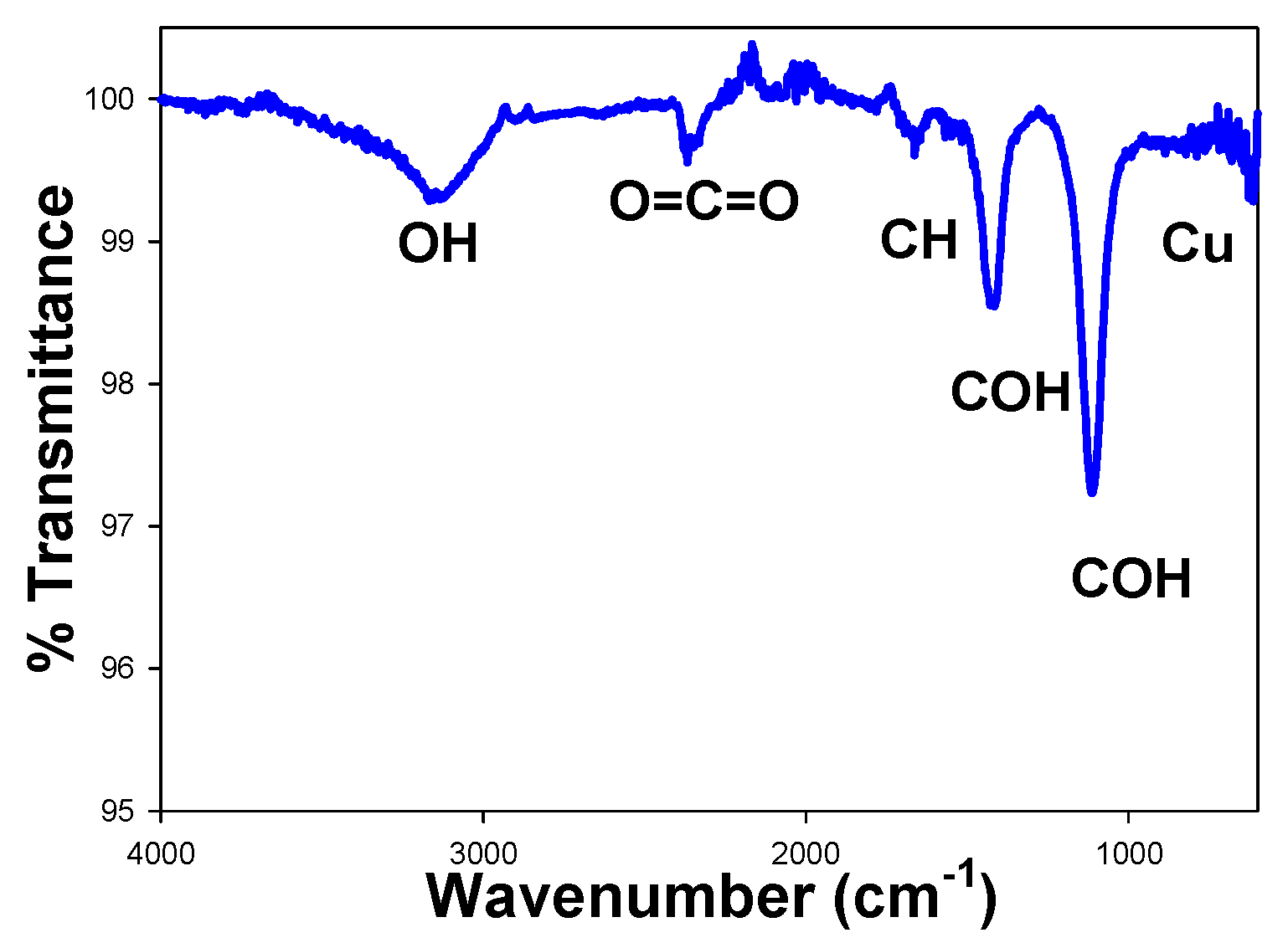
3.2.1. FTIR and UV-Vis for Cu NPs
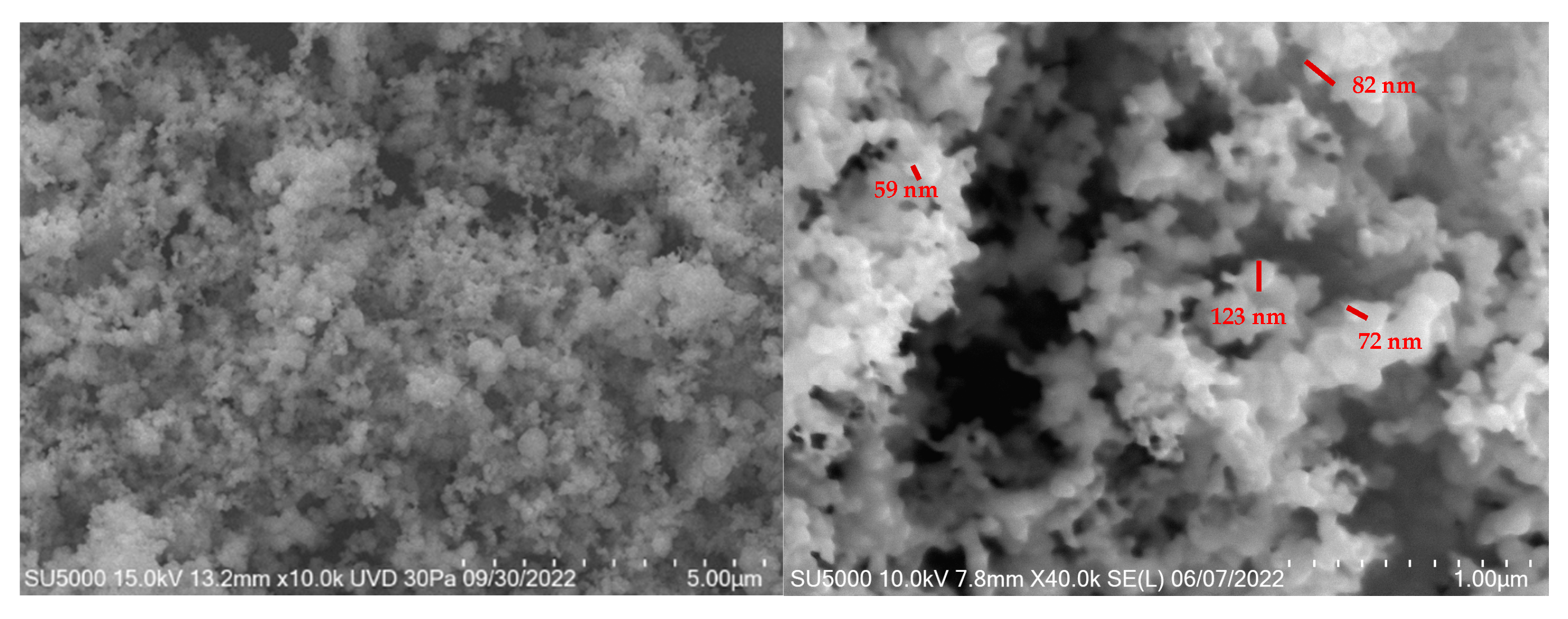
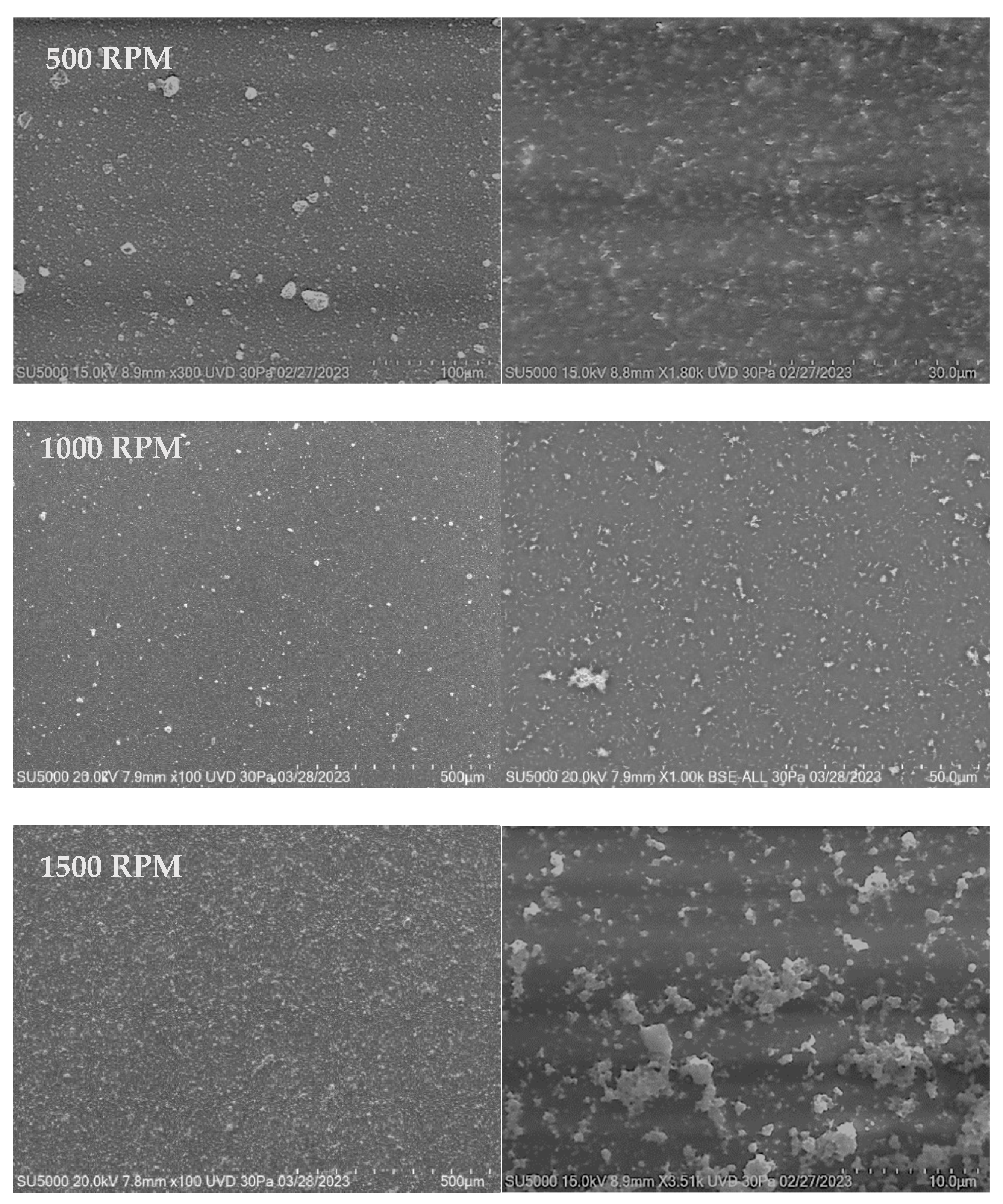
3.2.2. SEM
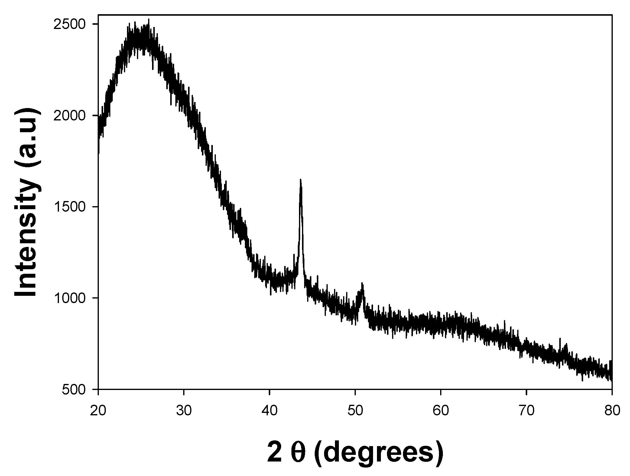
3.2.3. XRD
3.3. PVA-Cu Nanocomposite Films
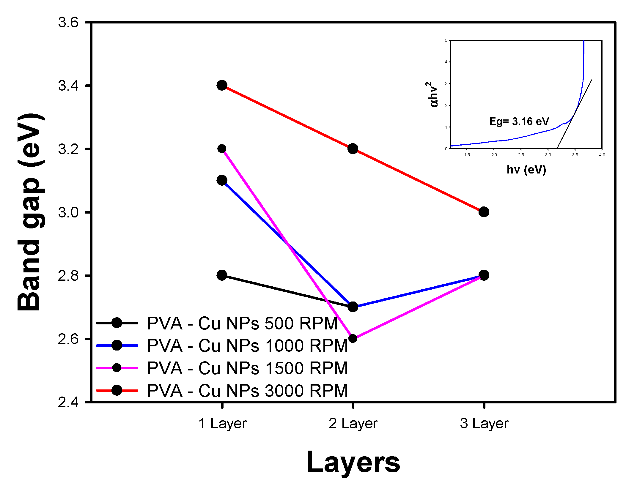
3.3.1. UV-Vis
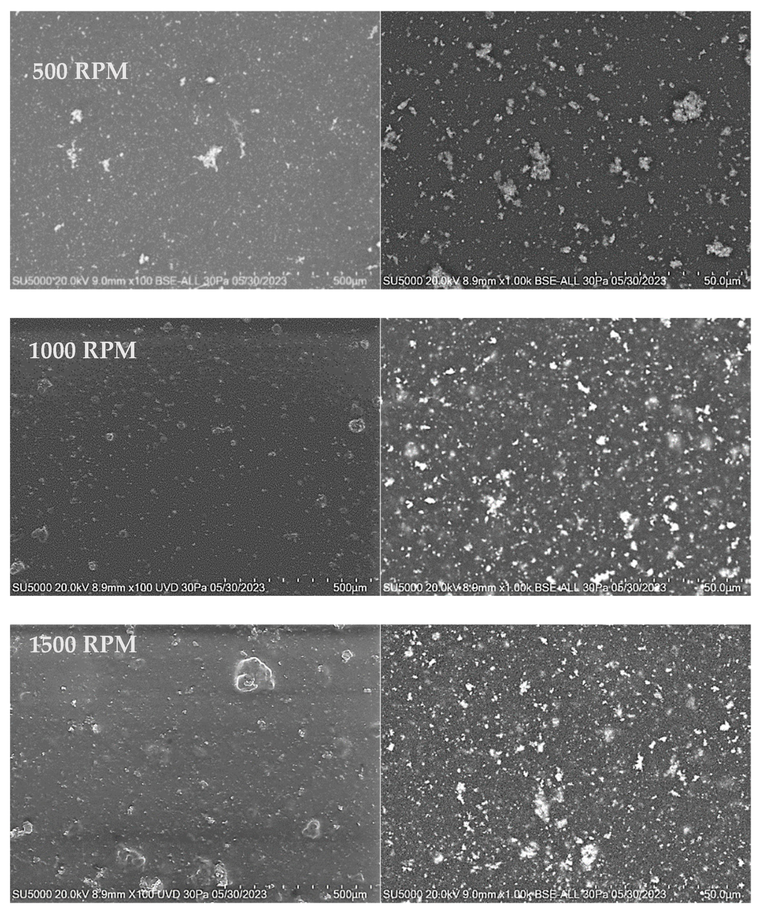
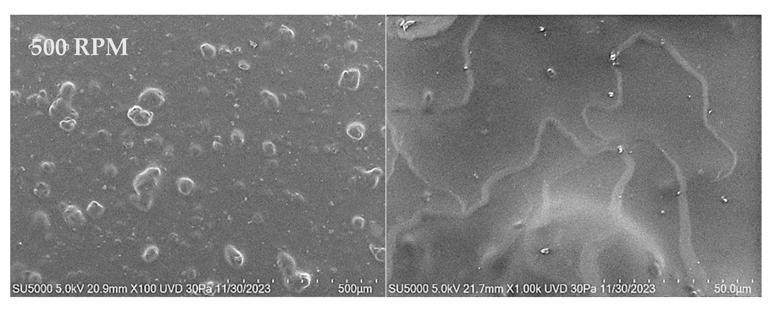
3.3.2. SEM
3.3.3. XRD
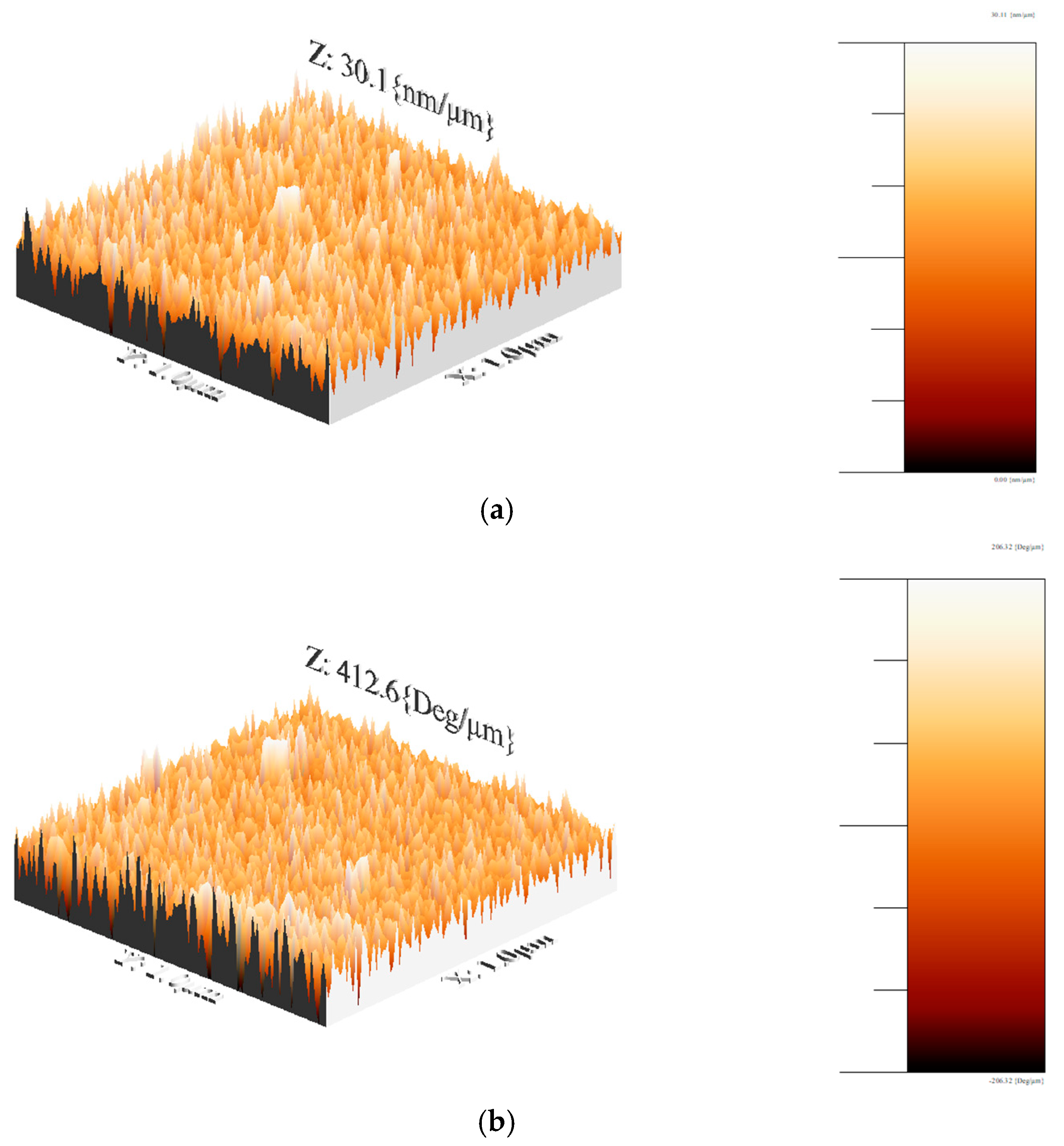
3.3.4. AFM
3.3.5. I–V Curves
4. Conclusions
Author Contributions
Funding
Institutional Review Board Statement
Informed Consent Statement
Data Availability Statement
Conflicts of Interest
References
- Parveen, F.; Sannakki, B.; Mandke, M.V.; Pathan, H.M. Copper nanoparticles: Synthesis methods and its light harvesting performance. Sol. Energy Mater. Sol. Cells 2016, 144, 371–382. [Google Scholar] [CrossRef]
- Rydosz, A. The use of copper oxide thin films in gas-sensing applications. Coatings 2018, 8, 425. [Google Scholar] [CrossRef]
- Zhong, J.; Xiang, W.; Zhao, H.; Zhao, W.; Chen, G.; Liang, X. Synthesis, characterization, and third-order nonlinear optical properties of copper quantum dots embedded in sodium borosilicate glass. J. Alloys Comp. 2012, 537, 269–274. [Google Scholar] [CrossRef]
- Ali, M.K.A.; Xianjun, H. Colloidal stability mechanism of copper nanomaterials modified by ionic liquid dispersed in polyalphaolefin oil as green nanolubricants. J. Colloid. Interface Sci. 2020, 578, 24–36. [Google Scholar] [CrossRef]
- Maji, N.C.; Krishna, H.P.; Chakraborty, J. Low-cost and high-throughput synthesis of copper nanopowder for nanofluid applications. Chem. Eng. J. 2018, 353, 34–45. [Google Scholar] [CrossRef]
- Yong, Y.; Yonezawa, T.; Matsubara, M.; Tsukamoto, H. The mechanism of alkylamine-stabilized copper fine particles towards improving the electrical conductivity of copper films at low sintering temperature. J. Mater. Chem. C Mater. 2015, 3, 5890–5895. [Google Scholar] [CrossRef]
- Di Bernardo, I.; Bradford, J.; Fusco, Z.; Mendoza, J.; Tran-Phu, T.; Bo, R.; Motta, N.; Tricoli, A. Self-assembly of noble metal-free graphene-copper plasmonic metasurfaces. J. Mater. Chem. C Mater. 2020, 8, 11896–11905. [Google Scholar] [CrossRef]
- Qing, X.; Shi, J.; Ma, C.; Fan, M.; Bai, Z.; Chen, Z.; Qiao, J.; Zhang, J. Simultaneous formation of nitrogen and sulfur-doped transition metal catalysts for oxygen reduction reaction through pyrolyzing carbon-supported copper phthalocyanine tetrasulfonic acid tetrasodium salt. J. Power Sour. 2014, 266, 88–98. [Google Scholar] [CrossRef]
- Nasrollahzadeh, M.; Babaei, F.; Fakhri, P.; Jaleh, B. Synthesis, characterization, structural, optical properties and catalytic activity of reduced graphene oxide/copper nanocomposites. RSC Adv. 2015, 5, 10782–10789. [Google Scholar] [CrossRef]
- Hejazy, M.; Koohi, M.K.; Pour, A.B.M.; Najafi, D. Toxicity of manufactured copper nanoparticles—A review. Nanomed. Res. J. 2018, 3, 1–9. [Google Scholar] [CrossRef]
- Hishimone, P.N.; Nagai, H.; Morita, M.; Sakamoto, T.; Sato, M. Highly-conductive and well-adhered Cu thin film fabricated on quartz glass by heat treatment of a precursor film obtained via spray-coating of an aqueous solution involving Cu(II) complexes. Coatings 2018, 8, 352. [Google Scholar] [CrossRef]
- De la Pena, E.M.; Roy, S. Electrodeposited copper using direct and pulse currents from electrolytes containing low concentration of additives. Surf. Coat. Technol. 2018, 339, 101–110. [Google Scholar] [CrossRef]
- Ealia, S.A.M.; Saravanakumar, M.P. A review on the classification, characterization, synthesis of nanoparticles and their application. IOP Conf. Ser. Mater. Sci. Eng. 2017, 263, 032019. [Google Scholar] [CrossRef]
- Umer, A.; Naveed, S.; Ramzan, N.; Rafique, M.S. Selection of a suitable method for the synthesis of copper nanoparticles. Nano 2012, 7, 1230005. [Google Scholar] [CrossRef]
- Ou, H.; Shi, X.; Lu, Y.; Kollmuss, M.; Steiner, J.; Tabouret, V.; Syvajarvi, M.; Wellmann, P.; Chaussende, D. Novel Photonica Applications of Silicon Carbide. Materials 2023, 16, 1014. [Google Scholar] [CrossRef]
- Kaloyeros, A.E.; Goff, J.; Arkles, B. Defect-and H-free stoichiometric silicon carbide by thermal CVD from the single source precursor trisilacyclohexane. Electron. Mater. 2022, 3, 27–40. [Google Scholar] [CrossRef]
- Rozra, J.; Saini, I.; Sharma, A.; Chandak, N.; Aggarwal, S.; Dhiman, R.; Sharma, P.K. Cu nanoparticles induced structural, optical and electrical modification in PVA. Mater. Chem. Phys. 2012, 134, 1121–1126. [Google Scholar] [CrossRef]
- Fahmy, T.; Habib, A.; Sarhan, A.; Fahmy, T.; Habib, A.; Sarhan, A. Reparation and Investigation of PVA/Cu Nanoparticles by Eco-friendly Electrochemical Method. Res. Sq. 2022. [Google Scholar] [CrossRef]
- Kaloyeros, A.E.; Pan, Y.; Goff, J.; Arkles, B. Editors’ choice-review-cobalt thin films: Trends in processing technologies and emerging applications. ECS J. Solid. State Sci. Tecnol. 2019, 8, 119. [Google Scholar] [CrossRef]
- Al-Hakimi, A.N.; Asnag, G.M.; Alminderej, F.; Alhagri, I.A.; Al-Hazmy, S.M.; Qahtan, T.F. Enhancing the Structural, Optical, Thermal, and Electrical Properties of PVA Filled with Mixed Nanoparticles (TiO2/Cu). Crystals 2023, 13, 135. [Google Scholar] [CrossRef]
- Soliman, T.S.; Vshivkov, S.A. Effect of Fe nanoparticles on the structure and optical properties of polyvinyl alcohol nanocomposite films. J. Non-Cryst. Solids 2019, 519, 119452. [Google Scholar] [CrossRef]
- Joshi, A.; Mukherjee, G.S.; Banerjee, M.; Gupta, M. Effect of Ag underlayer on structural and optical properties of PVA/Ag/Co film. AIP Conf. Proc. 2020, 2220, 020073. [Google Scholar] [CrossRef]
- De Alba-Montero, I.; Guajardo-Pacheco, J.; Morales-Sánchez, E.; Araujo-Martínez, R.; Loredo-Becerra, G.M.; Martínez-Castañón, G.A.; Ruiz, F.; Compeán Jasso, M.E. Antimicrobial properties of copper nanoparticles and amino acid chelated copper nanoparticles produced by using a soya extract. Bioinorg. Chem. Appl. 2017. [Google Scholar] [CrossRef] [PubMed]
- Makula, P.; Pacia, M.; Macyk, W. How to correctly determine the band gap energy of modified semiconductor photocatalysts based on UV-Vis spectra. J. Phys. Chem. Lett. 2018, 9, 6814–6817. [Google Scholar] [CrossRef]
- Sabanci, S.; Kaya, K.; Goksu, A. Modeling the electrical conductivity value of the model solution. An. Acad. Bras. Cienc. 2023, 95, e20210062. [Google Scholar] [CrossRef]
- Aziz, S.B.; Ahmed, H.M.; Hussein, A.M.; Fathulla, A.B.; Wsw, R.M.; Hussein, R.T. Tuning the absorption of ultraviolet spectra and optical parameters of aluminum doped PVA based solid polymer composites. J. Mater. Sci. Mater. Electron. 2015, 26, 8022–8028. [Google Scholar] [CrossRef]
- Nimrodh Ananth, A.; Umapathy, S.; Sophia, J.; Mathavan, T.; Mangalaraj, D. On the optical and thermal properties of in situ/ex situ reduced Ag NP’s/PVA composites and its role as a simple SPR-based protein sensor. Appl. Nanosci. 2011, 1, 87–96. [Google Scholar] [CrossRef]
- Jubu, P.R.; Danladi, E.; Ndeze, U.I.; Adedokun, O.; Landi Jr, S.; Haider, A.J.; Adepoju, A.T.; Yusof, Y.; Obaseki, O.S.; Yam, F.K. Comment about the use of unconventional Tauc plots for bandgap energy determination of semiconductors using UV-Vis spectroscopy. Res. Opt. 2024, 14, 100606. [Google Scholar] [CrossRef]
- Thiruvengadam, M.; Chung, I.M.; Gomathi, T.; Ansari, M.A.; Gopiesh Khanna, V.; Babu, V.; Rajakumar, G. Synthesis, characterization and pharmacological potential of green synthesized copper nanoparticles. Bioprocess Biosyst. Eng. 2019, 42, 1769–1777. [Google Scholar] [CrossRef]
- Joseph, A.T.; Prakash, P.; Narvi, S.S. Phytofabrication and characterization of copper nanoparticles using allium sativum and its antibacterial activity. Int. J. Sci. Eng. Technol. 2016, 4, 2348–4098. [Google Scholar]
- Hasanin, M.; Al Abboud, M.A.; Alawlaqi, M.M.; Abdelghany, T.M.; Hashem, A.H. Ecofriendly Synthesis of Biosynthesized Copper Nanoparticles with Starch-Based Nanocomposite: Antimicrobial, Antioxidant, and Anticancer Activities. Biol. Trace Elem. Res. 2022, 200, 2099–2112. [Google Scholar] [CrossRef] [PubMed]
- Rodrigues, E.P.; Oliveira, L.C.; Silva, M.L.F.; Moreira, C.S.; Lima, A.M.N. Surface plasmon resonance sensing characteristics of thin copper and gold films in aqueous and gaseous interfaces. IEEE Sens. J. 2020, 20, 7701–7710. [Google Scholar] [CrossRef]
- Pérez-de León, A.; Plasencia, J.; Vázquez-Durán, A.; Méndez-Albores, A. Comparison of the in vitro antifungal and anti-fumonigenic activities of copper and silver nanoparticles against Fusilarium verticillioides. J. Clust. Sci. 2020, 31, 213–220. [Google Scholar] [CrossRef]
- Madhloom, S.D.; Mohsin, A.K.; Adem, K.A. Influence of Cu nanoparticles concentration on the electronic transition of pulsed laser deposited TiO2/ZnO: Cu nanocomposite film. Mater. Today Proc. 2021, 45, 5823–5828. [Google Scholar] [CrossRef]
- Priya, S.C.; Vijayalakshmi, S.; Raghavendra, S.G.; Yildizhan, S.; Ranjitha, J. A critical review on efficient photocatalytic degradation of organic compounds using copper-based nanoparticles. Mater. Today Proc. 2023, 80, 3075–3081. [Google Scholar] [CrossRef]
- Song, X.; Sun, S.; Zhang, W.; Yin, Z. A method for the synthesis of spherical copper nanoparticles in the organic phase. J. Colloid Interface Sci. 2004, 273, 463–469. [Google Scholar] [CrossRef]
- Gawande, M.B.; Goswami, A.; Felpin, F.X.; Asefa, T.; Huang, X.; Silva, R.; Zou, X.; Zboril, R.; Varma, R.S. Cu and Cu-based nanoparticles: Synthesis and applications in catalysis. Chem. Rev. 2016, 116, 3722–3811. [Google Scholar] [CrossRef]
- Amjad, R.; Mubeen, B.; Ali, S.S.; Imam, S.S.; Alshehri, S.; Ghoneim, M.M.; Alzarea, S.I.; Rasool, R.; Ullah, I.; Nadeem, M.S.; et al. Green synthesis and characterization of copper nanoparticles using Fortunella margarita leaves. Polymers 2021, 13, 4364. [Google Scholar] [CrossRef]
- Antonio-Pérez, A.; Durán-Armenta, L.F.; Pérez-Loredo, M.G.; Torres-Huerta, A.L. Biosynthesis of copper nanoparticles with medicinal plant extracts: From extraction methods to applications. Micromachines 2023, 14, 1882. [Google Scholar] [CrossRef]
- Aguilar, M.S.; Esparza, R.; Rosas, G. Synthesis of Cu nanoparticles by chemical reduction method. Trans. Nonfer. Met. Soc. China 2019, 29, 1510–1515. [Google Scholar] [CrossRef]
- Darwesh, A.H.A.; Aziz, S.B.; Hussen, S.A. Insights into optical band gap identification in polymer composite films based on PVA with enhanced optical properties: Structural and optical characteristics. Opt. Mater. 2022, 133, 113007. [Google Scholar] [CrossRef]
- Powar, N.S.; Patel, V.J.; Pagare, P.K.; Pandav, R.S. Chemical Methodologies Cu Nanoparticle: Synthesis, Characterization and Application Graphical Abstract. Chem. Meth. 2019, 3, 457–480. [Google Scholar] [CrossRef]
- Devi, S.R.; Saikia, P.J.; Hussain, M.A. Studies on optical and electrical properties of PVA capped nanocrystalline CdSe thin film prepared by chemical bath deposition method. Chalc. Lett. 2022, 19, 901–908. [Google Scholar] [CrossRef]
- El-Shamy, A.G. Composite (PVA/Cu nano) films: Two yield points, embedding mechanism and thermal properties. Prog. Org. Coat. 2019, 127, 252–259. [Google Scholar] [CrossRef]
- Aziz, S.B.; Abdulwahid, R.T.; Rasheed, M.A.; Abdullah, O.G.; Ahmed, H.M. Polymer blending as a novel approach for tuning the SPR peaks of silver nanoparticles. Polymers 2017, 9, 486. [Google Scholar] [CrossRef] [PubMed]
- Diani, J.; Gall, K. Properties of linear polylactic acid)/polyethylene glycol blends. Polym. Eng. Sci. 2012, 51, 108–116. [Google Scholar] [CrossRef]
- Mahendia, S.; Goyal, P.K.; Tomar, K.; Chahal, R.P.; Kumar, S. Study of Dielectric Behavior and Charge Conduction Mechanism of Poly(Vinyl Alcohol) (PVA)-Copper (Cu) and Gold (Au) Nanocomposites as a Bio-resorbable Material for Organic Electronics. J. Electron. Materials. 2016, 45, 5418–5426. [Google Scholar] [CrossRef]
- Ishaq, S.; Kanwala, F.; Atiqc, S.; Moussab, M.; Azharb, U.; Guld, I.; Losic, D. Dielectric and impedance spectroscopic studies of three phase graphene/titania/poly(vinyl alcohol) nanocomposite films. Res. Phys. 2018, 11, 540–548. [Google Scholar] [CrossRef]
- Mohammed, M.I.; Yahia, I.S.; El-Sayed, F. Study the microstructure, optical, mechanical, and dielectric characteristics of Cu2+/Zn2+-codoped PVA for CUT-OFF laser filters. Polym. Bullet. 2023, 80, 8377–8405. [Google Scholar] [CrossRef]
- Sanjay, V.; Rajashekara, K.M.; Johns, J.; Pattar, V. The dielectric and impedance spectroscopy of poly vinyl alcohol doped with carbon (PVA-C). Phys. B 2023, 650, 414561. [Google Scholar] [CrossRef]


| Sample | DC Conductivity (S/cm) | Reference |
|---|---|---|
| Pure PVA | 1.38 × 10⁻¹¹ | [46] |
| Pure PVA | 3.70 × 10⁻⁷ | [47] |
| PVA/Cu (0.09% wt.) | 5.80 × 10⁻¹⁰ | [48] |
| PVA/Cu (5% wt.) | 1.27 × 10⁻² | [49] |
| PVA-ZnS/Cu (5%) | 2.60 × 10⁻⁹ | [50] |
| PVA/Cu (5%), 500 RPM | 1.04 | This work |
| PVA/Cu (5%), 500 RPM | 9.40 × 10⁻¹ | This work |
| PVA/Cu (5%), 1000 RPM | 1.20 | This work |
| Sample | Dielectric Constant (ε) | Reference | |||
|---|---|---|---|---|---|
| 100 Hz | 1 kHz | 10 kHz | 100 kHz | ||
| Pure PVA | 5 | 2 | - | - | [46] |
| Pure PVA | -- | -- | -- | 2.38 | [47] |
| Pure PVA | 9.1 | 8.0 | 7.4 | -- | [48] |
| Pure PVA | 19.66 | 17.8 | -- | -- | [49] |
| Pure PVA | -- | 14.73 | -- | -- | [50] |
| PVA/Cu (0.09% wt.) | -- | -- | -- | 1.19 | [47] |
| PVA/Cu (4% wt.) | 34.37 | 31.3 | -- | -- | [49] |
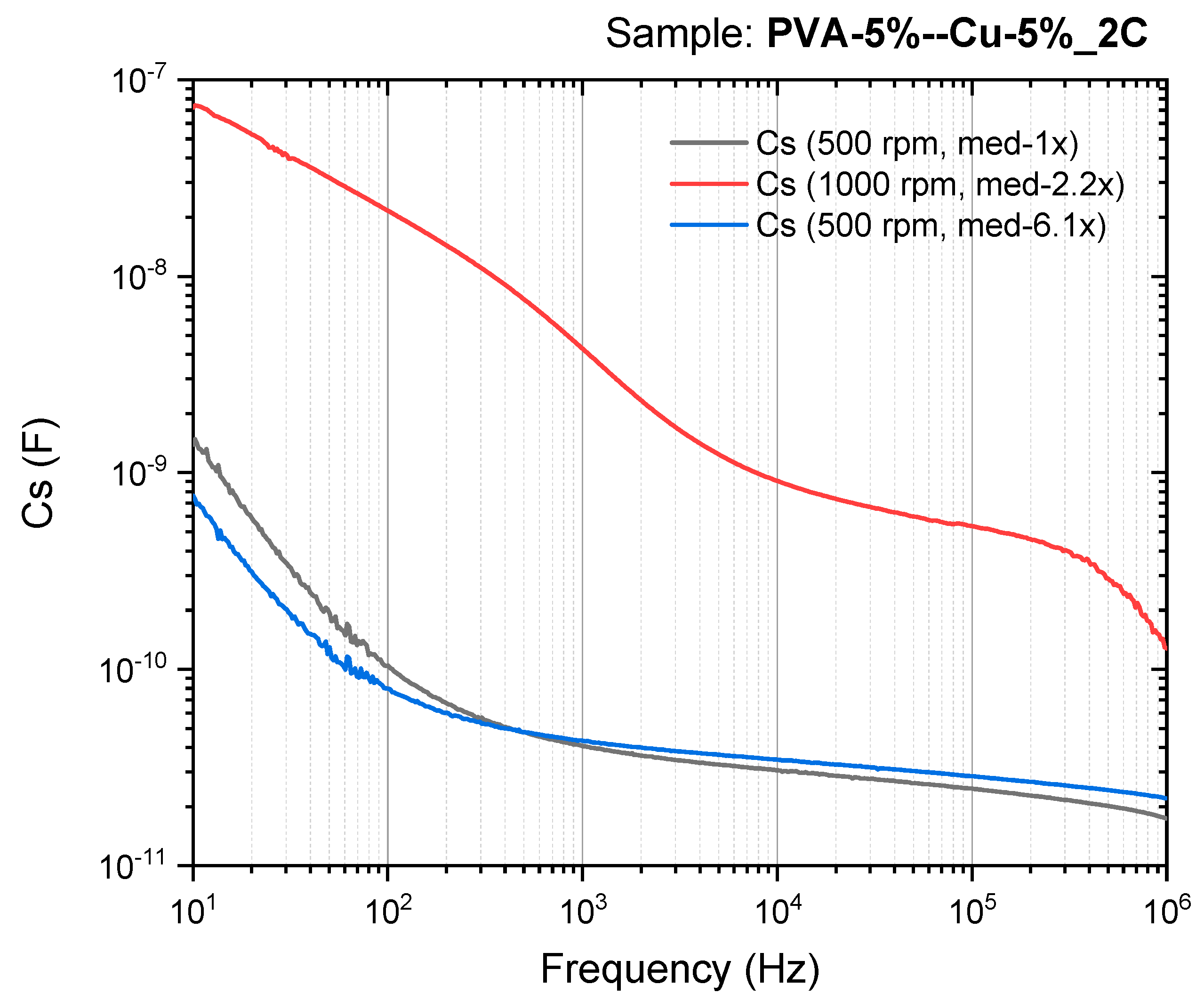
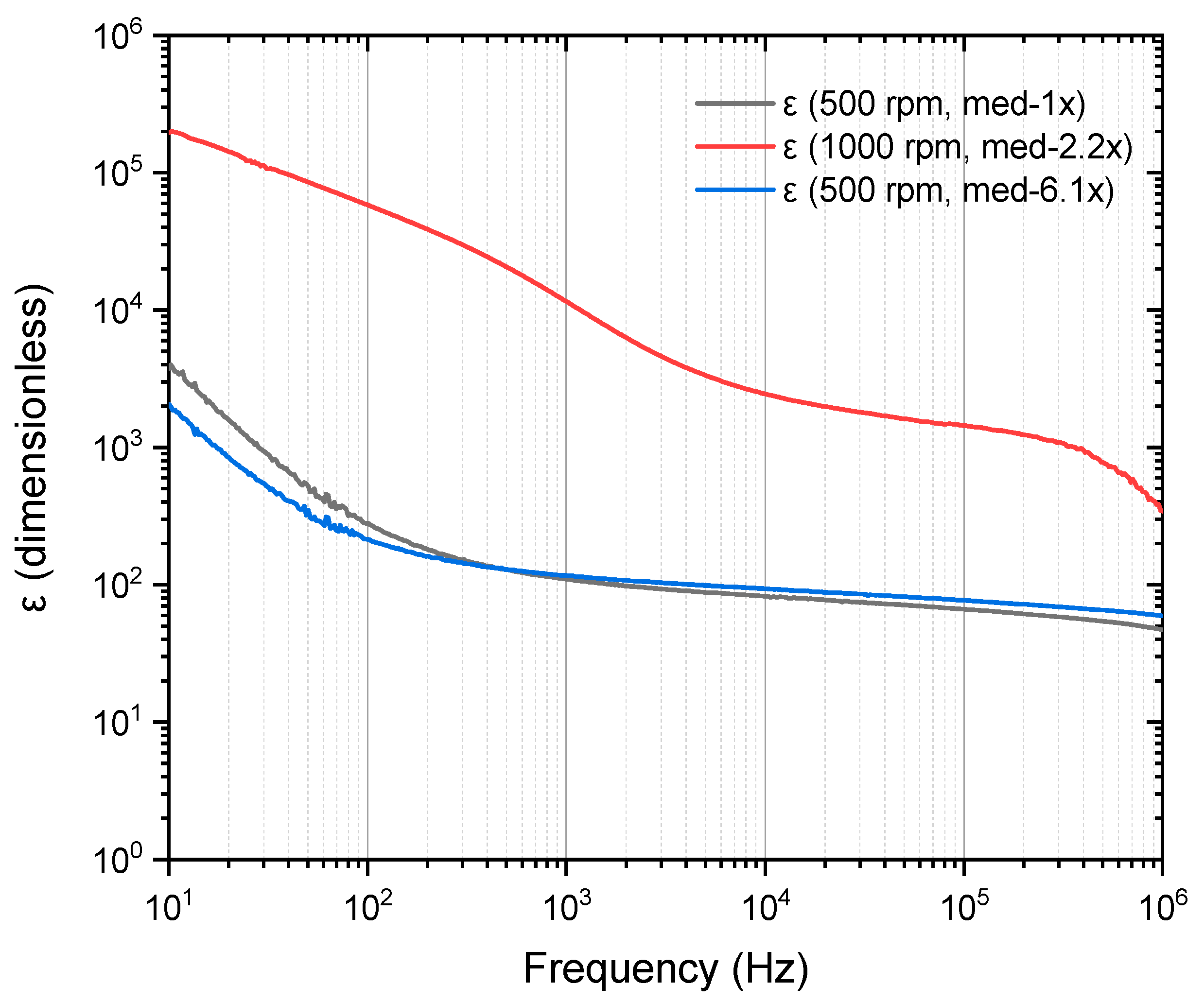
| PVA/Cu (5%), 500 RPM | 280.38 | 109.27 | 82.50 | 66.21 | This work |
| PVA/Cu (5%), 500 RPM | 214.73 | 116.46 | 93.52 | 76.82 | This work |
| PVA/Cu (5%), 1000 RPM | 58,004.1 | 11,453.4 | 2441.01 | 1438.43 | This work |
Disclaimer/Publisher’s Note: The statements, opinions and data contained in all publications are solely those of the individual author(s) and contributor(s) and not of MDPI and/or the editor(s). MDPI and/or the editor(s) disclaim responsibility for any injury to people or property resulting from any ideas, methods, instructions or products referred to in the content. |
© 2025 by the authors. Licensee MDPI, Basel, Switzerland. This article is an open access article distributed under the terms and conditions of the Creative Commons Attribution (CC BY) license (https://creativecommons.org/licenses/by/4.0/).
Share and Cite
Hernández, M.A.A.; Ascencio Hurtado, C.; Garcia, F.C.; Lázaro, R.C.A.; Ortega, M.A.C.; Arriaga, C.A.A.; Castillo, A.C. Enhanced Structural, Optical, Electrical, and Dielectric Properties of PVA/Cu Nanocomposites for Potential Applications in Flexible Electronics. Materials 2025, 18, 2087. https://doi.org/10.3390/ma18092087
Hernández MAA, Ascencio Hurtado C, Garcia FC, Lázaro RCA, Ortega MAC, Arriaga CAA, Castillo AC. Enhanced Structural, Optical, Electrical, and Dielectric Properties of PVA/Cu Nanocomposites for Potential Applications in Flexible Electronics. Materials. 2025; 18(9):2087. https://doi.org/10.3390/ma18092087
Chicago/Turabian StyleHernández, Marco A. Alaniz, Carlos Ascencio Hurtado, Filiberto Candia Garcia, Roberto C. Ambrosio Lázaro, Manuel A. Chairez Ortega, Cesar A. Arriaga Arriaga, and Amanda Carrillo Castillo. 2025. "Enhanced Structural, Optical, Electrical, and Dielectric Properties of PVA/Cu Nanocomposites for Potential Applications in Flexible Electronics" Materials 18, no. 9: 2087. https://doi.org/10.3390/ma18092087
APA StyleHernández, M. A. A., Ascencio Hurtado, C., Garcia, F. C., Lázaro, R. C. A., Ortega, M. A. C., Arriaga, C. A. A., & Castillo, A. C. (2025). Enhanced Structural, Optical, Electrical, and Dielectric Properties of PVA/Cu Nanocomposites for Potential Applications in Flexible Electronics. Materials, 18(9), 2087. https://doi.org/10.3390/ma18092087