
Oxygen Deficiency Modulated La-Doped BaSnO3 Films Showing Improved Light Transmittance


Abstract
1. Introduction
2. Materials and Methods
3. Results
3.1. XRD and RSM
3.2. STEM
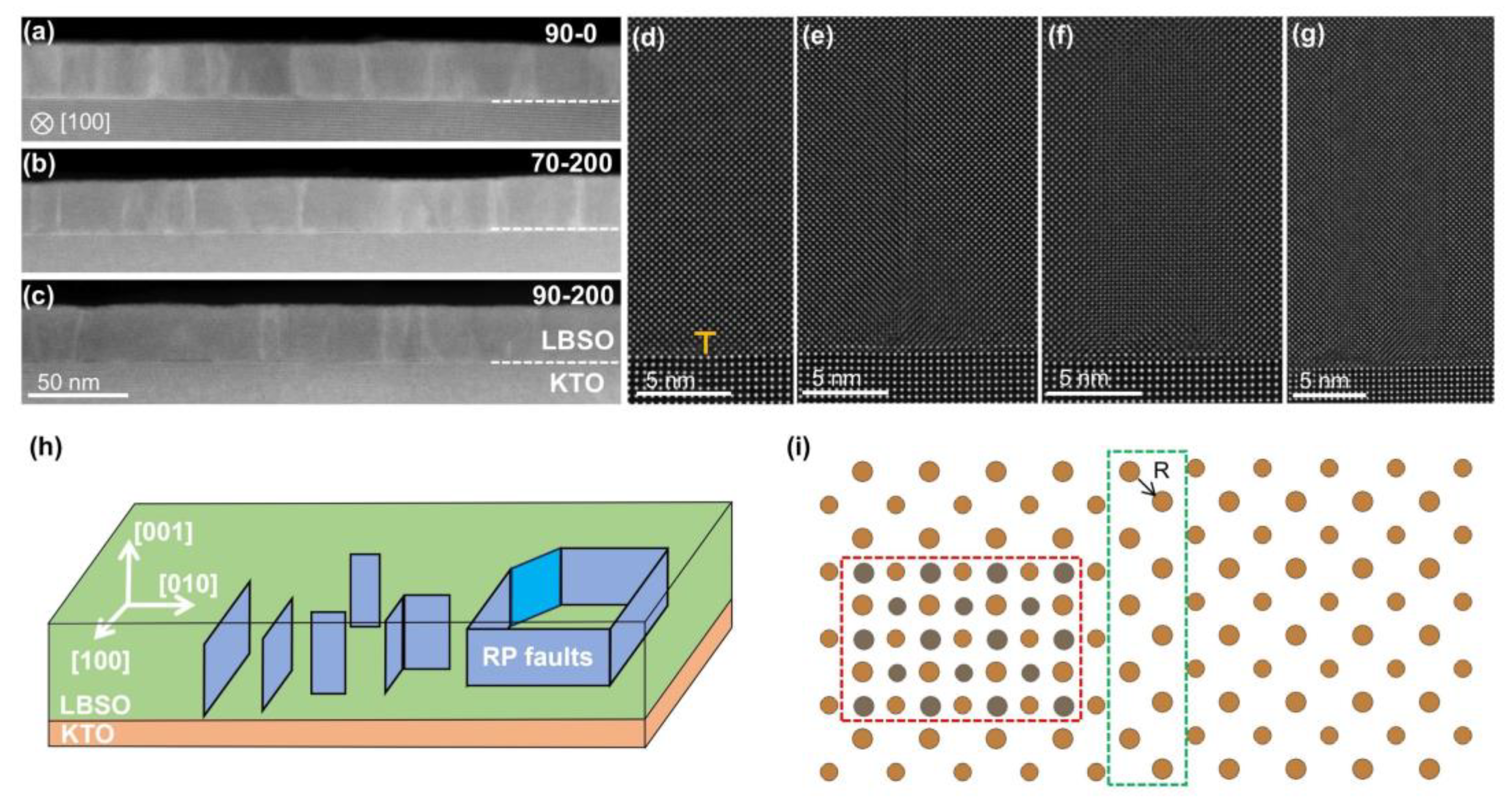
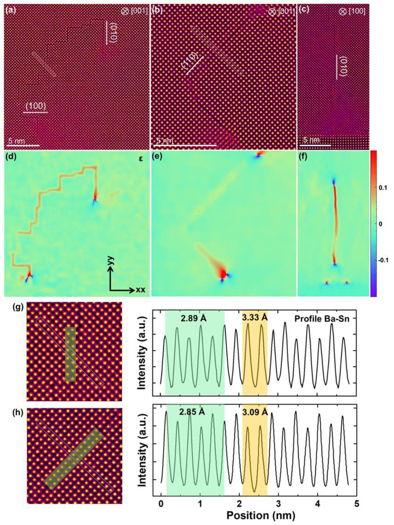
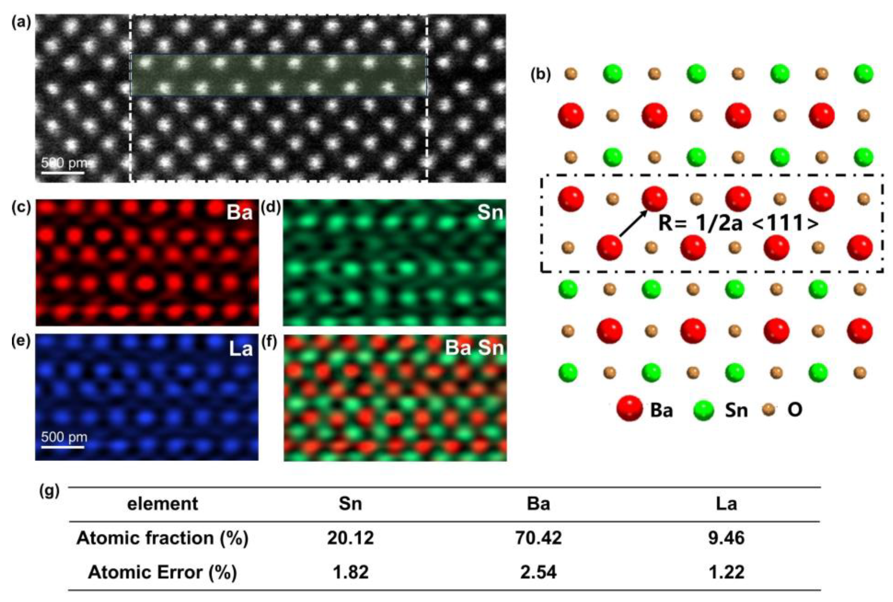
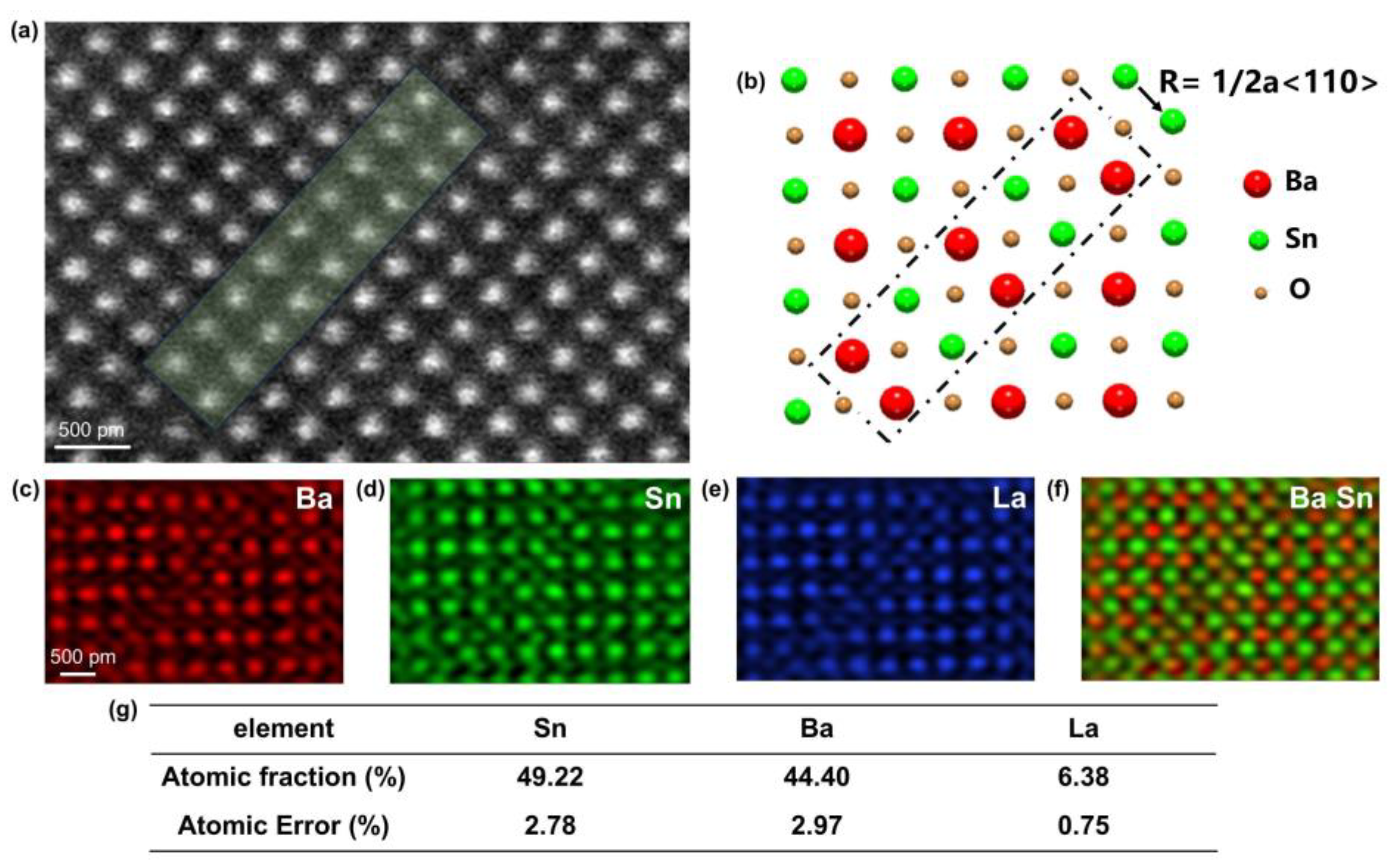
3.2.1. Cross-Section HAADF-STEM Images
3.2.2. In-Plane HAADF-STEM Images
3.3. EDS
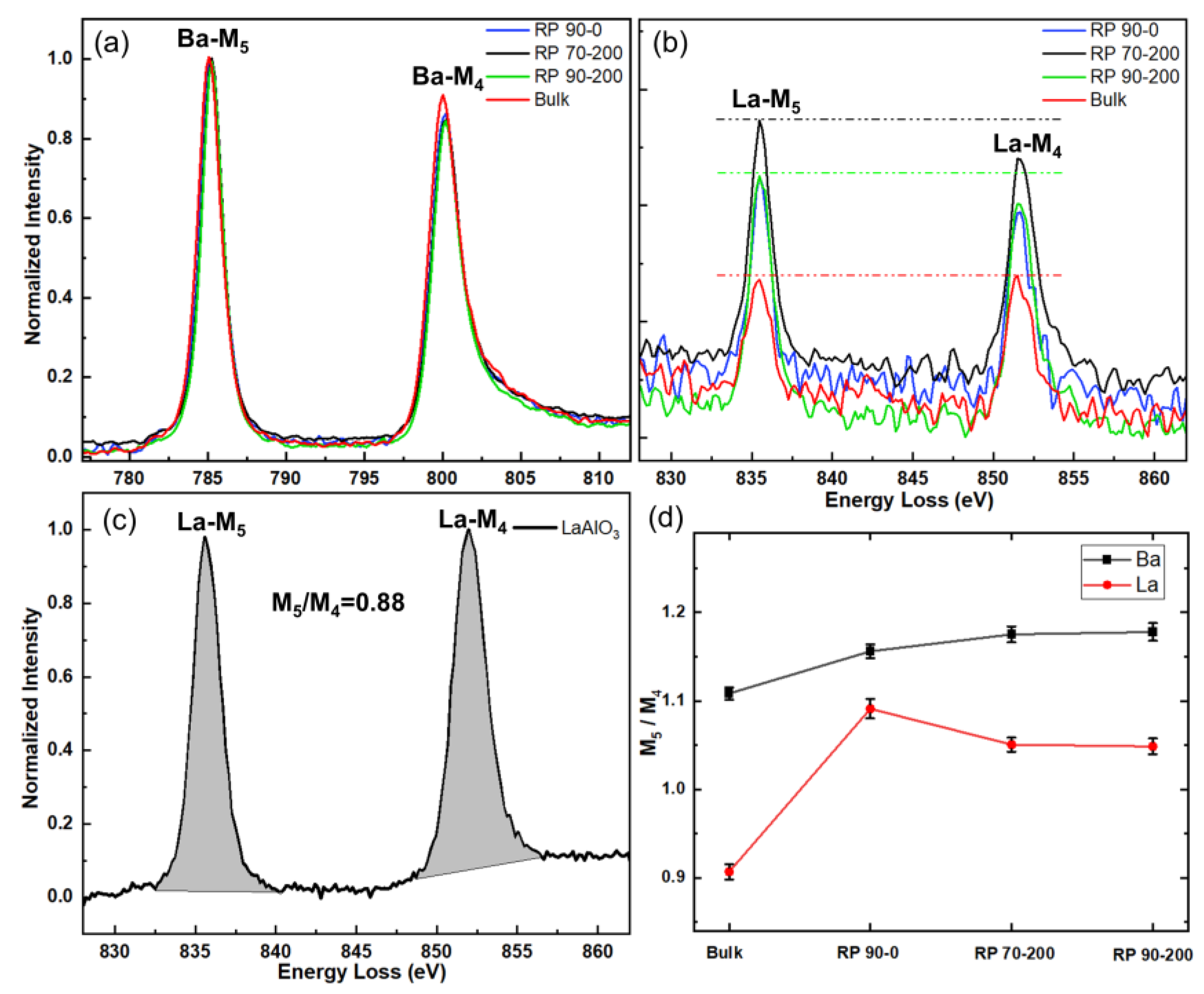
3.4. EELS
3.5. Optical Transmission
4. Discussion
5. Conclusions
Supplementary Materials
Author Contributions
Funding
Institutional Review Board Statement
Informed Consent Statement
Data Availability Statement
Conflicts of Interest
References
- Wang, Z.; Nayak, P.K.; Caraveo-Frescas, J.A.; Alshareef, H.N. Recent Developments in P-Type Oxide Semiconductor Materials and Devices. Adv. Mater. 2016, 28, 3831–3892. [Google Scholar] [CrossRef] [PubMed]
- Krishnaswamy, K.; Bjaalie, L.; Himmetoglu, B.; Janotti, A.; Gordon, L.; Van de Walle, C.G. BaSnO3 as a Channel Material in Perovskite Oxide Heterostructures. Appl. Phys. Lett. 2016, 108, 083501. [Google Scholar] [CrossRef]
- Das, S.; Jayaraman, V. SnO2: A Comprehensive Review on Structures and Gas Sensors. Prog. Mater. Sci. 2014, 66, 112–255. [Google Scholar] [CrossRef]
- Preissler, N.; Bierwagen, O.; Ramu, A.T.; Speck, J.S. Electrical Transport, Electrothermal Transport, and Effective Electron Mass in Single-Crystalline In2O3 Films. Phys. Rev. B 2013, 88, 085305. [Google Scholar] [CrossRef]
- Agashe, C.; Kluth, O.; Hüpkes, J.; Zastrow, U.; Rech, B.; Wuttig, M. Efforts to Improve Carrier Mobility in Radio Frequency Sputtered Aluminum Doped Zinc Oxide Films. J. Appl. Phys. 2004, 95, 1911–1917. [Google Scholar] [CrossRef]
- Nian, Q.; Zhang, M.Y.; Schwartz, B.D.; Cheng, G.J. Ultraviolet Laser Crystallized ZnO:Al Films on Sapphire with High Hall Mobility for Simultaneous Enhancement of Conductivity and Transparency. Appl. Phys. Lett. 2014, 104, 201907. [Google Scholar] [CrossRef]
- Kumar, A.; Zhou, C. The Race To Replace Tin-Doped Indium Oxide: Which Material Will Win? ACS Nano 2010, 4, 11–14. [Google Scholar] [CrossRef]
- Tu, G.; Wang, H.; Tu, B.; Xu, P.; Ren, L.; Huang, Q.; Yang, R.; Wang, W.; Fu, Z. Achieving Near-Theoretical Transmittance in MgAl2O4 Ceramic at Reduced Sintering Temperature via Solution Substitution. J. Eur. Ceram. Soc. 2025, 45, 117382. [Google Scholar] [CrossRef]
- Tu, G.; Xu, P.; Chen, B.; Yang, M.; Jing, Z.; Gao, P.; Tu, B.; Wang, H.; Wang, W.; Fu, Z. Reaction-Sintered Highly Transparent MgGa2O4 Ceramics with Enhanced Dielectric Properties. J. Eur. Ceram. Soc. 2025, 45, 117024. [Google Scholar] [CrossRef]
- Ferrara, M.C.; Montecchi, M.; Mittiga, A.; Schioppa, M.; Mazzarelli, S.; Tapfer, L.; Lovergine, N.; Prete, P. Synthesis and Annealing Effects on Microstructure and Optical Properties of Wide-Bandgap Polycrystalline Ferro-Pseudobrookite FeTi2O5 Sol-Gel Layers. Ceram. Int. 2025, 51, 9669–9676. [Google Scholar] [CrossRef]
- Theanmozhi, M.; Sasikumar, K.; Michael, R.J.V. Influence of Blocking Layer on Hf and V Doped Perovskite Structured SrSnO3 for Highly Efficient Dye-Sensitized Solar Cells. Ceram. Int. 2025, 51, 10383–10394. [Google Scholar] [CrossRef]
- Ngabonziza, P.; Nono Tchiomo, A.P. Epitaxial Films and Devices of Transparent Conducting Oxides: La:BaSnO3. APL Mater. 2024, 12, 120601. [Google Scholar] [CrossRef]
- Prakash, A.; Xu, P.; Faghaninia, A.; Shukla, S.; Ager, J.W.; Lo, C.S.; Jalan, B. Wide Bandgap BaSnO3 Films with Room Temperature Conductivity Exceeding 104 S cm−1. Nat. Commun. 2017, 8, 15167. [Google Scholar] [CrossRef] [PubMed]
- Raghavan, S.; Schumann, T.; Kim, H.; Zhang, J.Y.; Cain, T.A.; Stemmer, S. High-Mobility BaSnO3 Grown by Oxide Molecular Beam Epitaxy. APL Mater. 2016, 4, 016106. [Google Scholar] [CrossRef]
- Lee, W.-J.; Kim, H.J.; Sohn, E.; Kim, T.H.; Park, J.-Y.; Park, W.; Jeong, H.; Lee, T.; Kim, J.H.; Choi, K.-Y.; et al. Enhanced Electron Mobility in Epitaxial (Ba,La)SnO3 Films on BaSnO3 (001) Substrates. Appl. Phys. Lett. 2016, 108, 082105. [Google Scholar] [CrossRef]
- Kim, H.J.; Kim, U.; Kim, H.M.; Kim, T.H.; Mun, H.S.; Jeon, B.-G.; Hong, K.T.; Lee, W.-J.; Ju, C.; Kim, K.H.; et al. High Mobility in a Stable Transparent Perovskite Oxide. Appl. Phys. Express 2012, 5, 061102. [Google Scholar] [CrossRef]
- Nomura, K.; Ohta, H.; Ueda, K.; Kamiya, T.; Hirano, M.; Hosono, H. Thin-Film Transistor Fabricated in Single-Crystalline Transparent Oxide Semiconductor. Science 2003, 300, 1269–1272. [Google Scholar] [CrossRef]
- Kim, H.M.; Kim, U.; Park, C.; Kwon, H.; Char, K. Thermally Stable Pn-Junctions Based on a Single Transparent Perovskite Semiconductor BaSnO3. APL Mater. 2016, 4, 056105. [Google Scholar] [CrossRef]
- Zhu, L.; Shao, Z.; Ye, J.; Zhang, X.; Pan, X.; Dai, S. Mesoporous BaSnO3 Layer Based Perovskite Solar Cells. Chem. Commun. 2016, 52, 970–973. [Google Scholar] [CrossRef]
- Gurusinghe, M.N.; Andersson, T.G. Mobility in Epitaxial GaN: Limitations of Free-Electron Concentration Due to Dislocations and Compensation. Phys. Rev. B 2003, 67, 235208. [Google Scholar] [CrossRef]
- You, J.H.; Lu, J.-Q.; Johnson, H.T. Electron Scattering Due to Threading Edge Dislocations in N-Type Wurtzite GaN. J. Appl. Phys. 2006, 99, 033706. [Google Scholar] [CrossRef]
- Cho, H.J.; Onozato, T.; Wei, M.; Sanchela, A.; Ohta, H. Effects of Vacuum Annealing on the Electron Mobility of Epitaxial La-Doped BaSnO3 Films. APL Mater. 2019, 7, 022507. [Google Scholar] [CrossRef]
- Yoon, D.; Yu, S.; Son, J. Oxygen Vacancy-Assisted Recovery Process for Increasing Electron Mobility in n-Type BaSnO3 Epitaxial Thin Films. NPG Asia Mater. 2018, 10, 363–371. [Google Scholar] [CrossRef]
- Cui, J.; Zhang, Y.; Wang, J.; Zhao, Z.; Huang, H.; Zou, W.; Yang, M.; Peng, R.; Yan, W.; Huang, Q.; et al. Oxygen Deficiency Induced Strong Electron Localization in Lanthanum Doped Transparent Perovskite Oxide BaSnO3. Phys. Rev. B 2019, 100, 165312. [Google Scholar] [CrossRef]
- Luo, B.; Hu, J. Unraveling the Oxygen Effect on the Properties of Sputtered BaSnO3 Thin Films. ACS Appl. Electron. Mater. 2019, 1, 51–57. [Google Scholar] [CrossRef]
- Ganguly, K.; Prakash, A.; Jalan, B.; Leighton, C. Mobility-Electron Density Relation Probed via Controlled Oxygen Vacancy Doping in Epitaxial BaSnO3. APL Mater. 2017, 5, 056102. [Google Scholar] [CrossRef]
- Shi, S.; Xi, H.; Cao, T.; Lin, W.; Liu, Z.; Niu, J.; Lan, D.; Zhou, C.; Cao, J.; Su, H.; et al. Interface-Engineered Ferroelectricity of Epitaxial Hf0.5Zr0.5O2 Thin Films. Nat. Commun. 2023, 14, 1780. [Google Scholar] [CrossRef]
- Li, C.; Wang, L.; Xu, L.; Ren, X.; Yao, F.; Lu, J.; Wang, D.; Liang, Z.; Huang, P.; Wu, S.; et al. Mn-Inlaid Antiphase Boundaries in Perovskite Structure. Nat. Commun. 2024, 15, 6735. [Google Scholar] [CrossRef]
- Bae, I.-T.; Lingley, Z.R.; Foran, B.J.; Adams, P.M.; Paik, H. Large Bi-Axial Tensile Strain Effect in Epitaxial BiFeO3 Film Grown on Single Crystal PrScO3. Sci. Rep. 2023, 13, 19018. [Google Scholar] [CrossRef]
- Li, C.; Wang, L.; Wang, Z.; Yang, Y.; Ren, W.; Yang, G. Atomic Resolution Interfacial Structure of Lead-Free Ferroelectric K0.5Na0.5NbO3 Thin Films Deposited on SrTiO3. Sci. Rep. 2016, 6, 37788. [Google Scholar] [CrossRef]
- Paik, H.; Chen, Z.; Lochocki, E.; Seidner, A.H.; Verma, A.; Tanen, N.; Park, J.; Uchida, M.; Shang, S.; Zhou, B.-C.; et al. Adsorption-Controlled Growth of La-Doped BaSnO3 by Molecular-Beam Epitaxy. APL Mater. 2017, 5, 116107. [Google Scholar] [CrossRef]
- Yun, H.; Ganguly, K.; Postiglione, W.; Jalan, B.; Leighton, C.; Mkhoyan, K.A.; Jeong, J.S. Microstructure Characterization of BaSnO3 Thin Films on LaAlO3 and PrScO3 Substrates from Transmission Electron Microscopy. Sci. Rep. 2018, 8, 10245. [Google Scholar] [CrossRef]
- Yun, H.; Topsakal, M.; Prakash, A.; Jalan, B.; Jeong, J.S.; Birol, T.; Mkhoyan, K.A. Metallic Line Defect in Wide-Bandgap Transparent Perovskite BaSnO3. Sci. Adv. 2021, 7, eabd4449. [Google Scholar] [CrossRef] [PubMed]
- Wang, W.Y.; Tang, Y.L.; Zhu, Y.L.; Suriyaprakash, J.; Xu, Y.B.; Liu, Y.; Gao, B.; Cheong, S.-W.; Ma, X.L. Atomic Mapping of Ruddlesden-Popper Faults in Transparent Conducting BaSnO3-Based Thin Films. Sci. Rep. 2015, 5, 16097. [Google Scholar] [CrossRef]
- Lu, Y.; Yang, C.; Wang, H.; Ma, L.; Xu, M.; Xi, L. Structure, Principle, and Application of Magnetic Field-Assisted Pulsed Laser Deposition: An Overview. Vacuum 2023, 211, 111912. [Google Scholar] [CrossRef]
- Pennycook, S.J.; Rafferty, B.; Nellist, P.D. Z-Contrast Imaging in an Aberration-Corrected Scanning Transmission Electron Microscope. Microsc. Microanal. 2000, 6, 343–352. [Google Scholar] [CrossRef]
- Gázquez, J.; Sánchez-Santolino, G.; Biškup, N.; Roldán, M.A.; Cabero, M.; Pennycook, S.J.; Varela, M. Applications of STEM-EELS to Complex Oxides. Mater. Sci. Semicond. Process. 2017, 65, 49–63. [Google Scholar] [CrossRef]
- Sheeraz, M.; Ahn, C.W.; Duong, N.X.; Hwang, S.-Y.; Jang, J.-S.; Kim, E.-Y.; Kim, Y.K.; Lee, J.; Jin, J.S.; Bae, J.-S.; et al. Protonation-Driven Polarization Retention Failure in Nano-Columnar Lead-Free Ferroelectric Thin Films. Adv. Sci. 2024, 11, 2408784. [Google Scholar] [CrossRef]
- Hÿtch, M.J.; Snoeck, E.; Kilaas, R. Quantitative Measurement of Displacement and Strain Fields from HREM Micrographs. Ultramicroscopy 1998, 74, 131–146. [Google Scholar] [CrossRef]
- Bartels, W.J.; Hornstra, J.; Lobeek, D.J.W. X-Ray Diffraction of Multilayers and Superlattices. Acta Crystallogr. Sect. A 1986, 42, 539–545. [Google Scholar] [CrossRef]
- Kim, T.H.; Paudel, T.R.; Green, R.J.; Song, K.; Lee, H.-S.; Choi, S.-Y.; Irwin, J.; Noesges, B.; Brillson, L.J.; Rzchowski, M.S.; et al. Strain-Driven Disproportionation at a Correlated Oxide Metal-Insulator Transition. Phys. Rev. B 2020, 101, 121105. [Google Scholar] [CrossRef]
- Jaim, H.M.I.; Lee, S.; Zhang, X.; Takeuchi, I. Stability of the Oxygen Vacancy Induced Conductivity in BaSnO3 Thin Films on SrTiO3. Appl. Phys. Lett. 2017, 111, 172102. [Google Scholar] [CrossRef]
- Bak, J.; Chung, S.-Y. Observation of Fault-Free Coherent Layer during Ruddlesden–Popper Faults Generation in LaNiO3 Thin Films. J. Korean Ceram. Soc. 2021, 58, 169–177. [Google Scholar] [CrossRef]
- Lu, C.J.; Bendersky, L.A.; Chang, K.; Takeuchi, I. High-Resolution Identification of ½⟨110⟩ Stacking Faults in Epitaxial Ba0.3Sr0.7TiO3 Thin Films. Philos. Mag. 2003, 83, 1565–1595. [Google Scholar] [CrossRef]
- Fleck, E.E.; Barone, M.R.; Nair, H.P.; Schreiber, N.J.; Dawley, N.M.; Schlom, D.G.; Goodge, B.H.; Kourkoutis, L.F. Atomic-Scale Mapping and Quantification of Local Ruddlesden–Popper Phase Variations. Nano Lett. 2022, 22, 10095–10101. [Google Scholar] [CrossRef]
- Kaminaga, K.; Oka, D.; Hasegawa, T.; Fukumura, T. Superconductivity of Rock-Salt Structure LaO Epitaxial Thin Film. J. Am. Chem. Soc. 2018, 140, 6754–6757. [Google Scholar] [CrossRef]
- Sun, P.-H.; Zhang, J.-F.; Liu, K.; Han, Q.; Lu, Z.-Y. First-Principles Study of the Superconductivity in LaO. Phys. Rev. B 2021, 104, 045121. [Google Scholar] [CrossRef]
- Vattuone, L.; Savio, L.; Rocca, M. High Resolution Electron Energy Loss Spectroscopy (HREELS): A Sensitive and Versatile Surface Tool. In Surface Science Techniques; Bracco, G., Holst, B., Eds.; Springer: Berlin/Heidelberg, Germany, 2013; pp. 499–529. ISBN 978-3-642-34243-1. [Google Scholar]
- Zhang, Y.; Chen, J.; Li, K.; Wu, H.; Hu, Z.; Wang, J.; Wu, Y.; Yu, H. LaMg6Ga6S16: A Chemical Stable Divalent Lanthanide Chalcogenide. Nat. Commun. 2024, 15, 2959. [Google Scholar] [CrossRef]
- Tang, Y.L.; Zhu, Y.L.; Liu, Y.; Wang, Y.J.; Ma, X.L. Giant Linear Strain Gradient with Extremely Low Elastic Energy in a Perovskite Nanostructure Array. Nat. Commun. 2017, 8, 15994. [Google Scholar] [CrossRef]
- Sankaralingam, S.; Jaya, S.M.; Pari, G.; Asokamani, R. The Electronic Structure and Superconductivity of the Lanthanum Monochalcogenides LaX (X = S, Se, Te). Phys. Status Solidi 1992, 174, 435–447. [Google Scholar] [CrossRef]
- Qian, J.; Shen, Z.; Wei, X.; Li, W. Z_2 Nontrivial Topology of Rare-Earth Binary Oxide Superconductor LaO. Phys. Rev. B 2022, 105, L020508. [Google Scholar] [CrossRef]


| 90 mT-200 T | 70 mT-200 T | 90 mT-0 T | |
|---|---|---|---|
| out-of-plane | 4.14 Å | 4.14 Å | 4.13 Å |
| in-plane | 4.09 Å | 4.09 Å | 4.10 Å |
Disclaimer/Publisher’s Note: The statements, opinions and data contained in all publications are solely those of the individual author(s) and contributor(s) and not of MDPI and/or the editor(s). MDPI and/or the editor(s) disclaim responsibility for any injury to people or property resulting from any ideas, methods, instructions or products referred to in the content. |
© 2025 by the authors. Licensee MDPI, Basel, Switzerland. This article is an open access article distributed under the terms and conditions of the Creative Commons Attribution (CC BY) license (https://creativecommons.org/licenses/by/4.0/).
Share and Cite
Wu, K.; Geng, W.-R.; Zhu, Y.-L.; Ma, X.-L. Oxygen Deficiency Modulated La-Doped BaSnO3 Films Showing Improved Light Transmittance. Materials 2025, 18, 1696. https://doi.org/10.3390/ma18081696
Wu K, Geng W-R, Zhu Y-L, Ma X-L. Oxygen Deficiency Modulated La-Doped BaSnO3 Films Showing Improved Light Transmittance. Materials. 2025; 18(8):1696. https://doi.org/10.3390/ma18081696
Chicago/Turabian StyleWu, Kai, Wan-Rong Geng, Yin-Lian Zhu, and Xiu-Liang Ma. 2025. "Oxygen Deficiency Modulated La-Doped BaSnO3 Films Showing Improved Light Transmittance" Materials 18, no. 8: 1696. https://doi.org/10.3390/ma18081696
APA StyleWu, K., Geng, W.-R., Zhu, Y.-L., & Ma, X.-L. (2025). Oxygen Deficiency Modulated La-Doped BaSnO3 Films Showing Improved Light Transmittance. Materials, 18(8), 1696. https://doi.org/10.3390/ma18081696