Article

Improving Reliability of 1 Selector-1 ReRAM Crossbar Arrays Through Hybrid Switching Methods

Department of Artificial Intelligence Convergence, Sahmyook University, Seoul 01795, Republic of Korea
*
Author to whom correspondence should be addressed.
Materials 2025, 18(4), 761; https://doi.org/10.3390/ma18040761
Submission received: 31 December 2024 / Revised: 30 January 2025 / Accepted: 8 February 2025 / Published: 9 February 2025

Abstract

:
In this study, an innovative switching approach is explored to improve the reliability of 1 Selector-1 ReRAM (1S1R) devices, integrated into a 4K crossbar array (CBA). The key innovation is the use of DC sweeping for set operations and AC single-pulse resetting to minimize device stress and prevent breakdown. The selector, based on a GeSeTe ovonic threshold switching (OTS) element, demonstrated excellent endurance (>1012 cycles), fast switching (<100 ns), and high device-to-device uniformity (<5% variability). The ReRAM, constructed with Pt/LiNbOx/W, exhibited robust bipolar resistive switching, multi-bit capability, and endurance exceeding 1012 cycles. The integrated 1S1R CBA demonstrated reliable retention and low variability in operation, showing potential for high-performance, high-density memory applications.

1. Introduction

The increasing demand for high-density and energy-efficient memory solutions has positioned crossbar arrays (CBAs) as a promising architecture for next-generation memory devices. CBAs offer high integration density and scalability; however, challenges such as sneak currents and device reliability continue to hinder their widespread adoption. Sneak currents, which occur due to unintended current paths in unselected cells, degrade read/write accuracy and increase power consumption. Device reliability is also a significant concern, as repeated switching cycles can lead to material degradation and performance variability [1,2,3].
To address these challenges, the integration of a selector with resistive random-access memory (ReRAM) in a 1 Selector-1 ReRAM (1S1R) configuration has emerged as an effective solution. This configuration enhances read/write accuracy and minimizes sneak path currents by providing an inherent non-linearity in the current-voltage characteristics of the device. A typical 1S1R structure consists of an ovonic threshold switching (OTS) selector and a ReRAM cell. The OTS selector functions as a threshold-dependent switch that remains in a high-resistance state until a critical voltage is applied, effectively blocking leakage currents in unselected cells and preserving data integrity [4,5,6,7,8,9,10,11,12,13,14,15]. Meanwhile, the ReRAM cell provides reliable resistive switching behavior, enabling non-volatile data storage through controlled filament formation and rupture mechanisms [16,17,18,19,20,21,22,23,24,25,26,27,28,29,30,31]. Recent advances in material engineering and device structuring have further improved the scalability and performance of 1S1R arrays, making them more suitable for commercial applications [32,33,34].
Despite these advances, conventional 1S1R devices still face challenges, primarily due to the repeated application of high voltages during both set and reset operations. This continuous stress can accelerate material degradation, leading to potential breakdown and increased variability in device performance [35,36,37]. These reliability concerns become more pronounced in large-scale arrays, where consistent and uniform operation across multiple cells is critical [38,39,40,41,42]. Recent studies have proposed hybrid switching techniques to mitigate these issues, incorporating optimized pulse schemes to balance performance and endurance.
In this study, we propose a novel hybrid switching approach that employs DC sweeping for the set operation and an AC single-pulse for the reset process. The proposed method significantly reduces electrical stress during the reset phase, improving the device’s endurance and reliability. The effectiveness of this approach is validated using a GeSeTe-based OTS selector and a LiNbOx-based ReRAM, integrated into a 4K CBA. Our results demonstrate the potential of this hybrid switching technique for achieving high-performance and scalable memory applications, contributing to the advancement of next-generation non-volatile memory technologies.

2. Materials and Methods

2.1. Device Fabrication

The fabrication of the OTS device began with the deposition of a 30 nm tungsten (W) layer onto a Si/SiO2 substrate using physical vapor deposition (PVD). The bottom electrode (BE) pattern of the two-terminal unit cell was defined through photolithography and dry etching. Dry etching was performed using inductively coupled plasma reactive-ion etching (ICP-RIE) with an ICP source power of 300 W and a substrate bias power of 50 W. The etching gases included 4 sccm of argon (Ar) and 30 sccm of chlorine (Cl2), maintained at a process pressure of 5 mTorr. The etching rate was approximately 1 nm/min. After etching, residual photoresist (PR) was cleaned using acetone, isopropyl alcohol, and deionized (DI) water. A GeSeTe layer was then deposited using sputtering at 40 W radio frequency (RF) power, with a base pressure of 5 × 10⁻⁷ Torr and a working pressure of 2.8 mTorr. The sputtering process employed an Ar gas flow rate of 15 sccm. Finally, a 50 nm W top electrode (TE) was deposited through direct current (DC) magnetron sputtering after defining the TE pattern using photolithography and lift-off techniques. The DC sputtering process was performed at a base pressure of 1 × 10⁻⁶ Torr, a working pressure of 2.8 mTorr, and a DC power of 80 W with an Ar flow rate of 15 sccm. For the ReRAM device, a 100 nm platinum (Pt) layer was deposited on a Si/SiO2 substrate via PVD. The Pt bottom electrode patterning and etching processes followed the same procedure used for the OTS device with ICP source power of 350 W and a substrate bias power of 150 W. The etching gases included 4 sccm of Ar and 30 sccm of Cl2, maintained at a process of 3 mTorr. The etching rate was approximately 1 nm/min. After etching, residual PR was cleaned using acetone, isopropyl alcohol, and DI water. Subsequently, a TaOx switching layer was deposited by sputtering at 80 W RF power, with a base pressure of 5 × 10⁻⁷ Torr, a working pressure of 5 mTorr, an Ar flow rate of 20 sccm, and an oxygen (O2) flow rate of 15 sccm. Finally, a 50 nm W TE was deposited using the same method as employed for the OTS device. The 1S-1R structure was fabricated using a mask pattern different from the single-structure mask pattern described above, with the W TE of the fabricated ReRAM device simultaneously serving as the BE for the OTS selector. The OTS selector and the TE were deposited using the same methods as described above. This stepwise integration process ensured strong electrical contact and precise alignment between the OTS selector and the ReRAM device. The combined structure leveraged the OTS selector’s threshold switching capabilities and the ReRAM’s resistive switching characteristics, enabling efficient performance and scalability for high-density memory applications.

2.2. Electrical Measurements

Electrical characteristics of individual devices and the integrated 1S1R were assessed using a semiconductor parameter analyzer (SPA, Keithley 4200 SCS; Beaverton, OR, USA). During AC-based pulse operation, an arbitrary function generator (AFG, Agilent 81110A; Beaverton, OR, USA) and an RF electric-circuit switch box were used. The electrical pulses were generated by the AFG, and the conductance states were verified by the SPA. Most electrical measurements were executed at room temperature (25 °C), but the retention measurement was conducted at both room temperature and 85 °C. A hot stage using a temperature controller was employed to regulate the measurement temperature. During the synaptic operation of the ReRAM, the incremental step pulse programming (ISPP) method was adopted, in which incrementally increasing electrical pulses were applied to the device. Using this method, the ReRAM was potentiated or depressed to mimic the neuronal synaptic operation of the human brain. After applying the electrical pulse, a verifying step followed to obtain the conductance states of the device using SPA. All electrical measurements were performed using a LabVIEW™-based control program.

3. Results and Discussion

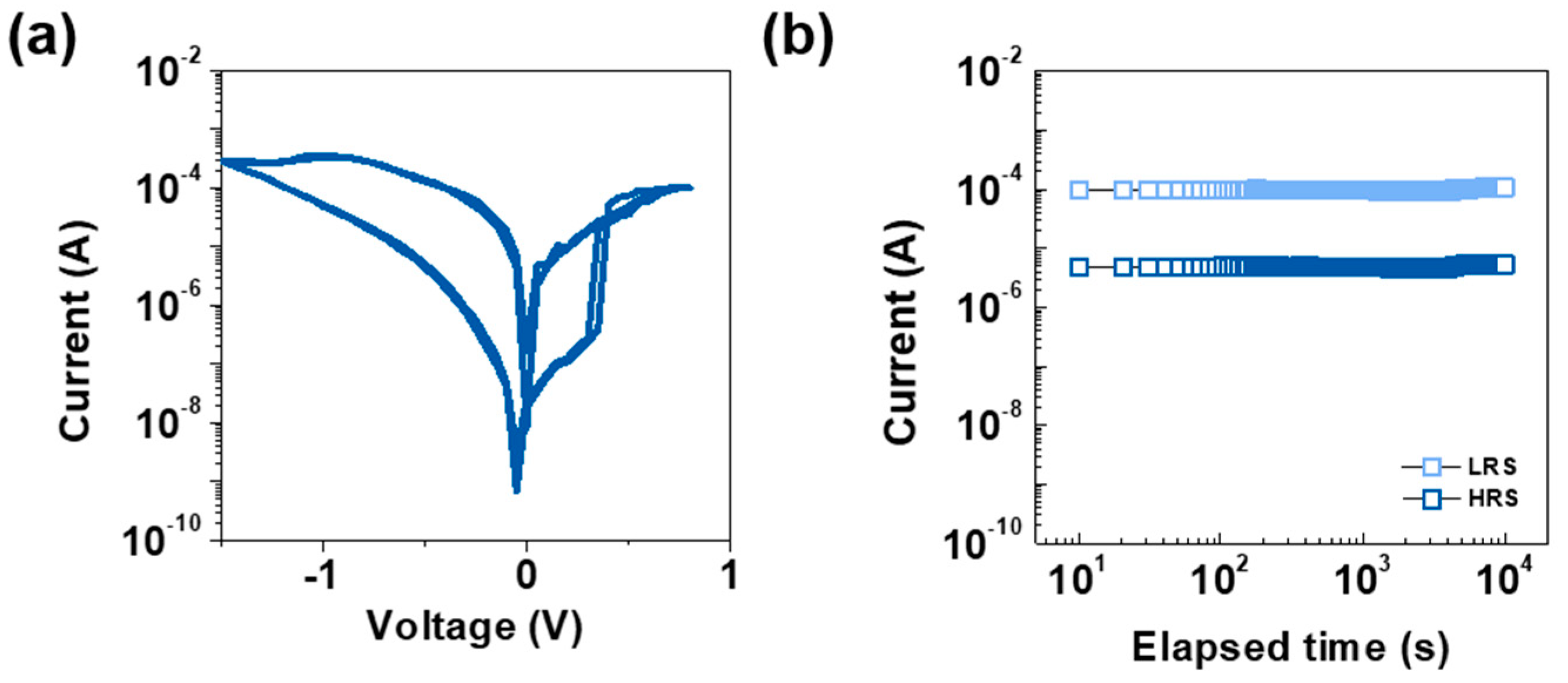
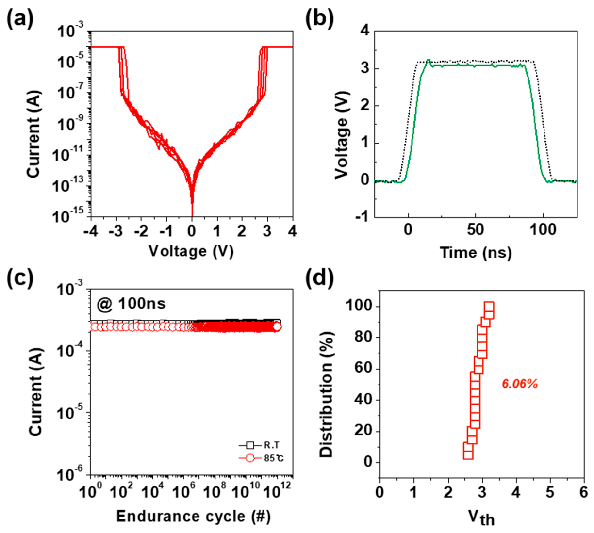
3.1. Characteristics of the ReRAM and OTS Devices

Figure 1 illustrates the electrical characteristics and retention properties of the Pt/LiNbOx/W-based ReRAM device. Figure 1a shows the DC I-V characteristics, demonstrating the bidirectional resistive switching behavior. The device transitions from the high-resistance state (HRS) to the low-resistance state (LRS) at a threshold voltage (Vth) of approximately ±0.3 V within a sweep voltage range of +0.8 V to −1.5 V. The sharp switching and low off-current observed confirm reliable resistive switching with minimal leakage. Figure 1b presents the retention characteristics of the device, measured at a read voltage (Vread) of −0.5 V. The current remains stable for both HRS and LRS over 104 s, indicating excellent data retention performance. These results confirm the Pt/LiNbOx/W-based ReRAM device’s suitability for non-volatile memory applications, with robust switching and reliable data storage capability. Figure 2 demonstrates the electrical performance and reliability of the Pt/LiNbOx/W-based ReRAM device.
In Figure 2a, the set switching behavior is shown with the device transitioning from the HRS to the LRS at approximately 1.8 V within 1 µs at a Vread of 0.02 V. Figure 2b highlights the reset switching, where the device returns from LRS to HRS at approximately −3 V within 1 µs. The endurance characteristics presented in Figure 2c show stable current levels for both HRS and LRS over 1012 cycles, confirming the device’s excellent reliability and robust cycling performance. Figure 2d shows the cumulative current distribution of 20 cells measured at −0.5 V, with a distribution ratio of 3.32% for HRS and 4.36% for LRS, indicating consistent and uniform switching behavior across the cells. Lastly, Figure 2e highlights the long-term potentiation (LTP) and long-term depression (LTD) characteristics under incremental step pulse programming (ISPP), where stable conductance modulation is observed over 200 pulses with pulse widths of 500 ns for LTP and 1 µs for LTD. These results demonstrate the high endurance, reliable switching characteristics, and synaptic behavior of the Pt/LiNbOx/W-based ReRAM device, making it a promising candidate for high-performance non-volatile memory and neuromorphic computing applications.
Figure 3a illustrates the DC I-V characteristics of the W/GeSeTe/W device, measured over an operating voltage of −4 V to 4 V. The graph demonstrates the bidirectional threshold switching behavior, with the Vth observed at approximately ±2.7 V. The current remains in the off-state (Ioff) with a leakage current of approximately 400 pA until the applied voltage reaches Vth, beyond which a rapid increase in current occurs, indicating the transition from HRS to LRS. Upon reducing the voltage, the device returns to its HRS, confirming the reversible switching behavior. Figure 3b presents the time-resolved voltage waveform applied to the OTS device during the switching operation. The applied waveform consists of a voltage pulse with a specific amplitude and duration, designed to induce the threshold switching behavior of the device. The graph demonstrates the voltage increase, stabilization at the peak level, and subsequent decrease over the course of the measurement. The application of this voltage pulse is crucial for analyzing the switching dynamics of the OTS device, as it provides insights into key performance parameters such as response time, threshold voltage stability, and write latency. The flat region at the peak voltage indicates the duration for which the applied voltage exceeds the Vth, allowing precise measurement of the time required for the device to transition from the HRS to the LRS. This transition time is a critical metric for evaluating the device’s suitability for high-speed memory applications. Moreover, the voltage waveform enables the assessment of switching consistency across multiple cycles, helping to identify potential variability and drift over prolonged operation. The ability to precisely control and optimize the switching time is essential for ensuring reliable and energy-efficient operation of selector devices in CBAs. Achieving minimal switching delay not only enhances the overall memory performance but also reduces power consumption, making the device suitable for high-density applications [43,44,45]. Additionally, understanding the temporal characteristics of the OTS device is critical for mitigating potential crosstalk or interference with neighboring memory cells, which is a common challenge in densely integrated memory arrays. By optimizing the applied waveform parameters, it is possible to improve the scalability and operational reliability of next-generation non-volatile memory technologies. These improvements and insights provided by the applied voltage waveform, as illustrated in Figure 3b, offer valuable guidance for optimizing the OTS device’s performance under various operating conditions and ensuring its practical application in advanced memory architectures. Figure 3c shows the endurance performance of the OTS device under 100 ns pulse operation at room temperature (RT) and elevated temperature (85 °C). The current remains stable over 1012 switching cycles, demonstrating excellent endurance and thermal stability. The minimal deviation in the current under high-temperature conditions indicates the robustness of the OTS device for operation in challenging environments. High endurance and thermal stability are essential for selector devices in high-density memory applications, as they ensure long-term reliability and performance under continuous stress. Furthermore, prolonged operation at high temperatures can induce atomic rearrangement within the OTS material, potentially affecting the stability of conduction pathways and the repeatability of switching characteristics. In particular, GeSeTe-based OTS materials are susceptible to phase transitions at elevated temperatures, which may lead to performance degradation. Therefore, the high-temperature endurance performance demonstrated in Figure 3c is significant, as it confirms the stability and reliability of the OTS device under conditions that could otherwise pose challenges to its operation [46,47]. These results confirm that the OTS device can withstand prolonged cycling without significant degradation, making it a strong candidate for use in next-generation memory technologies. Figure 3d presents the statistical distribution of the Vth for the OTS device, measured across 20 individual cells. The x-axis represents the Vth, while the y-axis shows the cumulative percentage distribution of the Vth values. The narrow spread of the Vth values, quantified by the standard deviation (6.06%), demonstrates the excellent uniformity and reliability of the device’s switching characteristics across multiple cells. This analysis is critical in the context of selector devices for high-density memory arrays, where consistent and predictable switching behavior across a large number of cells is essential for ensuring robust device operation. A narrow distribution of Vth values minimizes the variability, reducing the risk of unwanted interference or misoperation in crossbar architectures. Furthermore, the small variation in Vth indicates the stable material properties and device performance over repeated operations, even when measured across multiple cells. This consistency ensures long-term reliability in non-volatile memory applications. The observed uniformity in Vth distribution across the 20 cells highlights the suitability of the OTS device for use as a selector in memory arrays. Such uniformity enables the precise control of memory cell activation while suppressing sneak current paths, making it a strong candidate for achieving high yield and scalability in next-generation memory technologies.

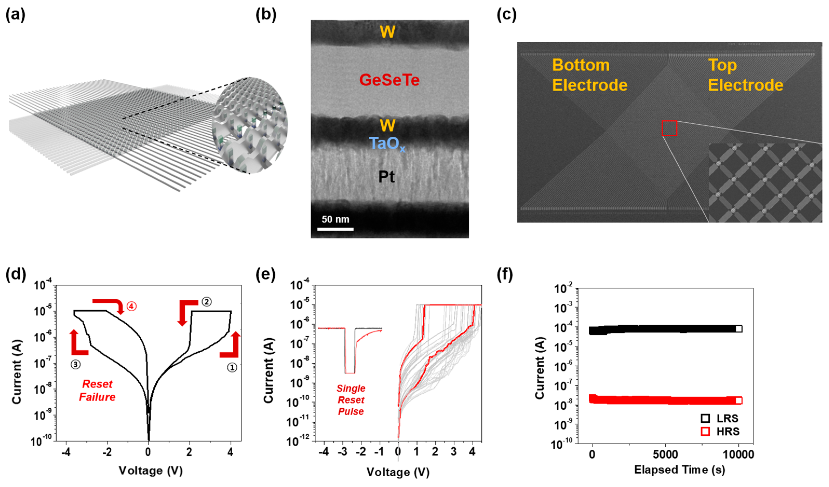
3.2. Integration and Performance of the 1S1R Device

Figure 4 illustrates the design, structural characterization, and electrical performance of the integrated 1S1R device implemented in a 4K CBA to enhance reliability through hybrid switching methods. Figure 4a presents a schematic of the 1S1R CBA, demonstrating its potential for high-density memory integration. Figure 4b shows the TEM (JEOL, Akishima, Japan) image of the 1S1R device structure, consisting of W/GeSeTe/W as the selector and Pt/TaOx/W as the memory element. The SEM (ZEISS, Jena, Germany) top-view image of the fabricated 4K CBA, displayed in Figure 4c, confirms the successful integration of the 1S1R architecture. Figure 4d shows the DC I-V characteristics of the 1S1R device with a compliance current (CC) of 1E-5 A. When operating under a bipolar DC sweep, the device transitions from HRS to LRS at point 1, and successfully returns to HRS at point 2 near 1.5 V. However, in the negative voltage region, although the device transitions to LRS at point 3, it fails to return to HRS at point 4, leading to performance degradation in subsequent cycles. This reset failure in the negative region hinders reliable device operation. To address this issue, a single reset pulse with a width of 1 µs and an amplitude of −5 V was applied, as shown in Figure 4e, successfully mitigating the reset failure and ensuring stable operation. This transition to single-pulse resetting represents a critical improvement in device reliability by enabling consistent switching performance. The hybrid switching approach, where the positive region sweep is maintained while employing a negative pulse for reset, prevents incomplete transitions and enhances device endurance. The negative pulse ensures that the device fully resets from LRS to HRS, thus improving overall reliability and preventing cumulative degradation. Finally, Figure 4f demonstrates the retention characteristics of the 1S1R device, measured at a read voltage of 2 V, where stable current levels for both LRS and HRS are maintained over 10,000 s. These results highlight the effectiveness of the hybrid switching method in improving the reliability of 1S1R CBAs, aligning with the focus in this study on optimizing reset operations through the integration of DC sweeps and single-pulse techniques.

4. Conclusions

In this work, a reliable 1S1R memory device integrated into a 4K CBA is demonstrated. The proposed novel switching scheme (DC sweep for setting and AC pulse for resetting) effectively reduces the device stress and prevents breakdown compared to conventional DC-only methods. By minimizing cumulative electrical stress during reset operations, this approach extends device endurance and operational lifespan, which is a critical improvement for large-scale memory applications. The integration of a GeSeTe-based selector and LiNbOx-based ReRAM provides a synergistic effect, achieving robust endurance, excellent retention, and low variability. Compared to traditional 1S1R architectures, the proposed hybrid switching method enables faster switching speeds and reduced power consumption, making it more suitable for next-generation high-density memory solutions. Furthermore, the reduction in reset failure rates and the improved uniformity across large memory arrays highlight the effectiveness of the hybrid switching scheme in addressing scalability challenges. These findings underscore the potential of 1S1R architectures with hybrid switching methods for next-generation memory technologies, offering a promising path toward efficient, reliable, and high-performance data storage solutions. Future works will focus on further optimizing the switching conditions and exploring the applicability of the proposed technique to even larger memory arrays and different material systems.

Author Contributions

Writing—original draft preparation, data curation, visualization, H.K.S.; writing—review and editing, supervision, funding acquisition, M.K.Y. All authors have read and agreed to the published version of the manuscript.

Funding

This work was supported by Institute of Information & communications Technology Planning & Evaluation (IITP) grant funded by the Korea government (MSIT) (RS-2024-00399394, Development of PDK and process integration platform for new memory-CMOS co-integrated PIM system).

Institutional Review Board Statement

Not applicable.

Informed Consent Statement

Not applicable.

Data Availability Statement

The original contributions presented in this study are included in the article. Further inquiries can be directed to the corresponding author.

Conflicts of Interest

The authors declare no conflicts of interest.

References

  1. Zhou, J.; Kim, K.H.; Lu, W. Crossbar RRAM arrays: Selector device requirements during read operation. IEEE Trans. Electron. Devices 2014, 61, 1369–1376. [Google Scholar] [CrossRef]
  2. Kim, K.-H.; Gaba, S.; Wheeler, D.; Cruz-Albrecht, J.M.; Hussain, T.; Srinivasa, N.; Lu, W. A Functional Hybrid Memristor Crossbar-Array/CMOS System for Data Storage and Neuromorphic Applications. Nano Lett. 2011, 12, 389–395. [Google Scholar] [CrossRef]
  3. Shi, L.; Zheng, G.; Tian, B.; Dkhil, B.; Duan, C. Research progress on solutions to the sneak path issue in memristor crossbar arrays. Nanoscale Adv. 2020, 2, 1811–1827. [Google Scholar] [CrossRef] [PubMed]
  4. Chen, Z.; Tong, H.; Li, X.; Wang, L.; Zhao, R.; Gu, W.; Miao, X. Experimental evidence for non-purely electric field induced threshold switching and modified thermal assisted model in GeTe phase change material. Appl. Phys. Lett. 2021, 118, 203502. [Google Scholar] [CrossRef]
  5. Anbarasu, M.; Wimmer, M.; Bruns, G.; Salinga, M.; Wuttig, M. Low power ovonic threshold switching characteristics of thin GeTe6 films using conductive atomic force microscopy. Appl. Phys. Lett. 2014, 105, 243501. [Google Scholar]
  6. Chien, W.-C.; Yeh, C.-W.; Bruce, R.L.; Cheng, H.-Y.; Kuo, I.T.; Yang, C.-H.; Ray, A.; Miyazoe, H.; Kim, W.; Carta, F.; et al. Toward ultimate nonvolatile resistive memories: The mechanism behind ovonic threshold switching revealed. Sci. Adv. 2020, 6, eaay2830. [Google Scholar]
  7. Jia, S.; Li, H.; Gotoh, T.; Longeaud, C.; Zhang, B.; Lyu, J.; Lv, S.; Zhu, M.; Song, Z.; Liu, Q.; et al. Ultrahigh drive current and large selectivity in GeS selector. Nat. Commun. 2020, 11, 4636. [Google Scholar] [CrossRef] [PubMed]
  8. Lelmini, D.; Zhang, Y. Analytical model for subthreshold conduction and threshold switching in chalcogenide-based memory devices. J. Appl. Phys. 2007, 102, 054517. [Google Scholar] [CrossRef]
  9. Adler, D.; Shur, M.S.; Silver, M.; Ovshinsky, S.R. Threshold switching in chalcogenide-glass thin films. J. Appl. Phys. 1980, 51, 3289–3309. [Google Scholar] [CrossRef]
  10. Velea, A.; Opsomer, K.; Devulder, W.; Dumortier, J.; Fan, J.; Detavernier, C.; Jurczak, M.; Govoreanu, B. Te-based chalcogenide materials for selector applications. Sci. Rep. 2017, 7, 8103. [Google Scholar] [CrossRef] [PubMed]
  11. Seo, H.K.; Ryu, J.J.; Lee, S.Y.; Park, M.; Park, S.-G.; Song, W.; Kim, G.H.; Yang, M.K. Material and Structural Engineering of Ovonic Threhold Switch for Highly Reliable Performance. Adv. Electron. Mater. 2022, 8, 2200161. [Google Scholar] [CrossRef]
  12. Seo, M.S.; Lee, S.W. Arsenic-free ovonic threshold switch for next-generation selectors in 3-dimensional cross-point memories. Mater. Commun. 2021, 29, 102849. [Google Scholar] [CrossRef]
  13. Seong, D.; Lee, S.Y.; Seo, H.K.; Kim, J.-W.; Park, M.; Yang, M.K. Highly Reliable Ovonic Threshold Switch with TiN/GeTe/TiN Structure. Materials 2023, 16, 2066. [Google Scholar] [CrossRef] [PubMed]
  14. Wang, L.; Cai, W.; He, D.; Lin, Q.; Wan, D.; Tong, H.; Miao, X. Performance Improvement of GeTex-Based Ovonic Threshold Switching Selector by C Doping. IEEE Electron Device Lett. 2021, 42, 688–691. [Google Scholar] [CrossRef]
  15. Lee, S.Y.; Seo, H.K.; Jeong, S.Y.; Yang, M.K. Improved Electrical Characteristics of Field Effect Transistors with GeSeTe-Based Ovonic Threshold Switching Devices. Materials 2023, 16, 4315. [Google Scholar] [CrossRef]
  16. Zhou, Y.X.; Li, Y.; Su, Y.T.; Wang, Z.R.; Shih, L.Y.; Chang, T.C.; Chang, K.C.; Long, S.B.; Sze, S.M.; Miao, X.S. Nonvolatile reconfgurable sequential logic in a HfO2 resistive random access memory array. Nanoscale 2017, 9, 6649–6657. [Google Scholar] [CrossRef] [PubMed]
  17. Lee, H.Y.; Lee, S.Y.; Lee, S.; Lee, S.; Kim, S.; Lee, D.; Cho, D.H.; Im, S. Filamentary resistive switching in ultra-thin amorphous carbon flm. Appl. Phys. Lett. 2009, 94, 232107. [Google Scholar]
  18. Lin, C.H.; Tsai, M.J.; Tsai, M.J.; Liao, M.J.; Wu, Y.H.; Chueh, Y.L.; King, Y.C. Filamentary and interface-type resistive switching in TiO -based resistive switching devices. Nanotechnology 2014, 25, 495201. [Google Scholar]
  19. Zhang, S.; Chen, S.; Huang, Y.; Chen, H. Filamentary resistive switching behavior in an interface-type ZnO resistive memory. J. Appl. Phys. 2011, 109, 124512. [Google Scholar]
  20. Ebadati, T.; Rahmanian, R.H.; Liu, Y.; Xia, Z.; Yang, J.J.; Xia, Q. Memristive synapses for efcient spiking neural networks: Flamentary versus homogene- ous resistive switching. IEEE Trans. Electron Devices 2021, 68, 4207–4214. [Google Scholar]
  21. Gao, F.; Wu, Y.; Liu, X.; Zhang, Z.; Li, L.; Huang, C.; Tan, C.; Chen, Y.; Song, L. Electroforming-free, low-power and high-reliability flamentary-based RRAM with improved endurance and retention. Microelectron. Eng. 2021, 247, 111437. [Google Scholar]
  22. Ullah, A.R.; Uddin, M.N.; Alim, A.; Hong, S.H.; Kim, S.J. Enhancement of bipolar flamentary resistive switching in Al/AlO/ITO RRAM devices by tuning the interface quality. J. Mater. Sci. Mater. Electron. 2021, 32, 7138–7145. [Google Scholar]
  23. Zhang, Z.; Luo, Y.; Liu, S.; Zhang, X.; Lu, W. Non-volatile resistive switching with flamentary mechanism in 3D-printed metal-organic framework devices. J. Mater. Chem. C 2021, 9, 3749–3755. [Google Scholar]
  24. Lu, M.; Huang, Y.; Zhang, X.; Wang, Y.; Chen, H. Filamentary resistive switching in nanocrystalline TiO films for resistive random access memory. J. Mater. Sci. Mater. Electron. 2021, 32, 18310–18317. [Google Scholar]
  25. Yao, J.; Liu, H.; Zhang, J.; Guo, H.; Zhu, X.; Hu, C.; Huang, R. Interface-type resistive switching memories. Adv. Mater. 2017, 29, 1606405. [Google Scholar]
  26. Jeong, J.; Lee, S.H.; Seo, D.H.; Lee, S.Y.; Kim, M.; Kim, K.M.; Jeon, J.H.; Lee, H.J.; Park, S.H. Interface-type resistive switching memory with nanoscale conductive flament. Adv. Mater. 2011, 23, 2060–2064. [Google Scholar]
  27. Han, T.; Liu, Y.; Xie, L.; Sun, H.; Wang, X.; Wang, X.; Liu, M. Intrinsic physical mechanism of interface-type resistive switching. Appl. Phys. Lett. 2021, 118, 193506. [Google Scholar]
  28. Liu, S.; Liu, H.; Zhang, Y.; Shi, S.; Du, L.; Chen, C.; Chen, Z.; Zhang, H. Highly uniform and stable resistive switching in interface-type HfO -based RRAM with novel electrode engineering. Appl. Phys. A 2021, 127, 850. [Google Scholar]
  29. Kim, W.; Park, S.; Kwon, Y.; Lee, H. Engineering the TiO2/Pt interface for improving the performance of interface-type RRAM devices. J. Electron. Mater. 2021, 50, 3359–3365. [Google Scholar]
  30. Kim, S.S.; Kim, S.J.; Seo, D.H.; Lee, J.W.; Park, J.; Jeong, Y.H.; Jang, J.; Lee, H.J. Enhanced memory performance of interface-type RRAM by surface modifcation of metal electrodes. IEEE Electron. Device Lett. 2021, 42, 163–166. [Google Scholar]
  31. Zhao, Z.; Zhang, Z.; Wu, X.; Li, L.; Liu, J.; Li, J.; Lu, Y. Highly uniform and stable interface-type resistive switching in HfO based RRAM with NiO embedded layer. Appl. Phys. Lett. 2021, 119, 193503. [Google Scholar]
  32. Lopez, J.M.; Rafhay, Q.; Dampfhoffer, M.; Reganaz, L.; Castellani, N.; Meli, V.; Martin, S.; Grenouillet, L.; Navarro, G.; Magis, T.; et al. 1S1R Optimization for High-Frequency Inference on Binarized Spiking Neural Networks. Adv. Electron. Mater. 2022, 8, 2200323. [Google Scholar] [CrossRef]
  33. Ambrosi, E.; Wu, C.H.; Song, M.; Lee, H.Y.; Li, K.S.; Lin, C.C.; Hsu, C.; Kuo, C.; Chang, W.N.; Chen, Y.J.; et al. Low voltage (<1.8 V) and high endurance (>1M) 1-Selector/1-STT-MRAM with ultra-low (1 ppb) read disturb for high-density embedded memory arrays. IEEE Int. Electron. Devices Meet. 2023, 1, 10413809. [Google Scholar]
  34. Hosseinzadeh, S.; Klemm, M.; Fischer, G.; Fey, D. Optimizing multi-level ReRAM memory for low latency and low energy consumption. Inf. Technol. 2023, 65, 52–64. [Google Scholar] [CrossRef]
  35. Tanaka, M.; Okayasu, S.; Shimizu, T.; Ito, T.; Shingubara, S. Conductance change property of the ReRAM with Au-doped HfOx switching layer under DC voltage pulses. In Proceedings of the IEEE Electron Devices Technology & Manufacturing Conference (EDTM), Bangalore, India, 3–6 March 2024; pp. 1–3. [Google Scholar]
  36. So, H.; Lee, J.; Mahata, C.; Kim, S.; Kim, S. Synaptic properties and short-term memory dynamics of TiO2/WOx heterojunction memristor for reservoir computing. Adv. Mater. Technol. 2024, 9, 2301390. [Google Scholar] [CrossRef]
  37. Al-Mamun, M.; Chakraborty, A.; Orlowski, M. Analysis of the electrical ReRAM device degradation induced by thermal cross-talk. Adv. Electron. Mater. 2023, 9, 2201081. [Google Scholar] [CrossRef]
  38. Cagli, C.; Sandrini, J.; Sassine, G.; Robayo, D.; Hammad, I.; Molas, G.; Gaillard, F. Reliability and scaling perspectives of HfO2-based OxRAM. ECS Meet. Abstr. 2020, 97, 9. [Google Scholar]
  39. Zhao, M.; Gao, B.; Yao, P.; Zhang, Q.; Zhou, Y.; Tang, J.; Qian, H.; Wu, H. Crossbar-level retention characterization in analog RRAM array-based computation-in-memory system. IEEE Trans. Electron Devices 2021, 68, 3813–3818. [Google Scholar] [CrossRef]
  40. Wiefels, S.; Kopperberg, N.; Hofmann, K.; Otterstedt, J.; Wouters, D.; Waser, R.; Menzel, S. Reliability aspects of 28 nm BEOL integrated ReRAM. Phys. Status Solidi A 2023, 221, 2300401. [Google Scholar] [CrossRef]
  41. Mao, M.; Chen, P.Y.; Yu, S.; Chakrabarti, C. A multilayer approach to designing energy-efficient and reliable ReRAM cross-point array system. IEEE Trans. VLSI Syst. 2017, 25, 1611–1621. [Google Scholar] [CrossRef]
  42. Mao, M.; Yu, C.; Chakrabarti, C. Optimizing latency, energy, and reliability of 1T1R ReRAM through cross-layer techniques. IEEE J. Emerg. Sel. Top. Circuits Syst. 2016, 6, 352–363. [Google Scholar] [CrossRef]
  43. Wang, X.; Qiao, R.; Lu, H.; He, W.; Liu, Y.; Zhou, T.; Wan, D.; Wang, Q.; Liu, Y.; Guo, W. 2D Memory Selectors with Giant Nonlinearity Enabled by Van der Waals Heterostructures. Small 2024, 20, e2310158. [Google Scholar] [CrossRef] [PubMed]
  44. Kim, K.H.; Seo, M.J.; Jang, B.C. Amorphous ITZO-Based Selector Device for Memristor Crossbar Array. Micromachines 2023, 14, 506. [Google Scholar] [CrossRef]
  45. Chen, P.H.; Lin, C.Y.; Chang, T.; Eshraghian, J.; Chao, Y.T.; Lu, W.; Sze, S. Investigating Selectorless Property within Niobium Devices for Storage Applications. ACS Appl. Mater. Interfaces 2022, 14, 2343–2350. [Google Scholar] [CrossRef] [PubMed]
  46. Wang, L.; Wen, J.; Liu, Z.; Chen, J.; Tong, H.; Miao, X. Thermally stable and high-speed Ge-Te based ovonic threshold switching selector with a Ge intercalated structure. IEEE Electron Device Lett. 2023, 44, 1096–1099. [Google Scholar] [CrossRef]
  47. Chen, J.; Wang, L.; Liu, Z.; Wen, J.; Tong, H.; Miao, X. Boron doping: Unlocking arsenic-mimicking performance in GeSe-based OTS selectors. IEEE Electron Device Lett. 2024, 45, 44–47. [Google Scholar] [CrossRef]
Figure 1. (a) DC I−V characteristics showing bidirectional resistive switching device behavior. (b) Retention performance demonstrating stable current levels for both HRS and LRS.
Materials 18 00761 g001
Figure 2. (a) Set operation characteristics and (b) reset operation characteristics of the Pt/LiNbOx/W device. (c) Endurance performance over multiple cycles. (d) Cumulative current distribution across multiple cells. (e) Synaptic behavior with stable conductance modulation.
Materials 18 00761 g002
Figure 3. (a) DC I−V characteristics showing bidirectional threshold switching behavior. (b) Voltage waveform used to evaluate switching dynamics. (c) Endurance performance over multiple cycles. (d) Statistical distribution of threshold voltage.
Materials 18 00761 g003
Figure 4. (a) Schematic of the 1S1R CBA. (b) TEM image of the 1S1R structure. (c) SEM top−view image of the fabricated 4k CBA. (d) DC I−V characteristics showing reset failure. (e) Stable operation achieved through single reset pulse. (f) Retention performance of the 1S1R device.
Materials 18 00761 g004
Disclaimer/Publisher’s Note: The statements, opinions and data contained in all publications are solely those of the individual author(s) and contributor(s) and not of MDPI and/or the editor(s). MDPI and/or the editor(s) disclaim responsibility for any injury to people or property resulting from any ideas, methods, instructions or products referred to in the content.

