Laser-Micro-Annealing of Microcrystalline Ni-Rich NCM Oxide: Towards Micro-Cathodes Integrated on Polyethylene Terephthalate Flexible Substrates

 , ,
, ,
Abstract
1. Introduction
2. Materials and Methods
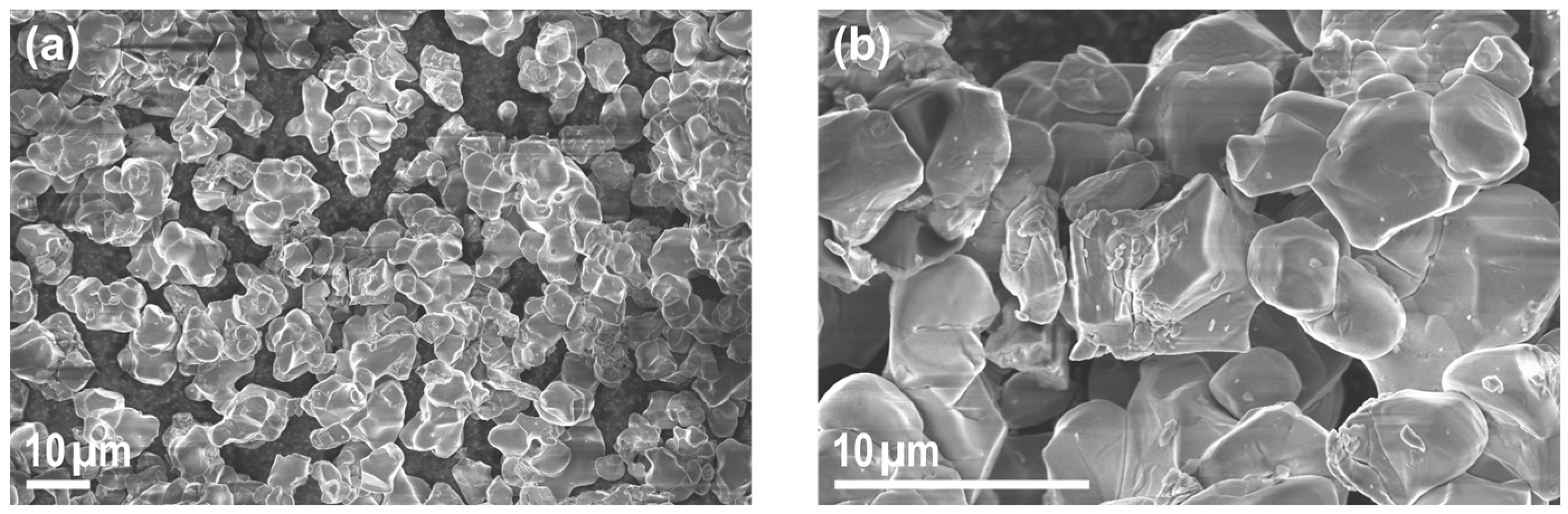
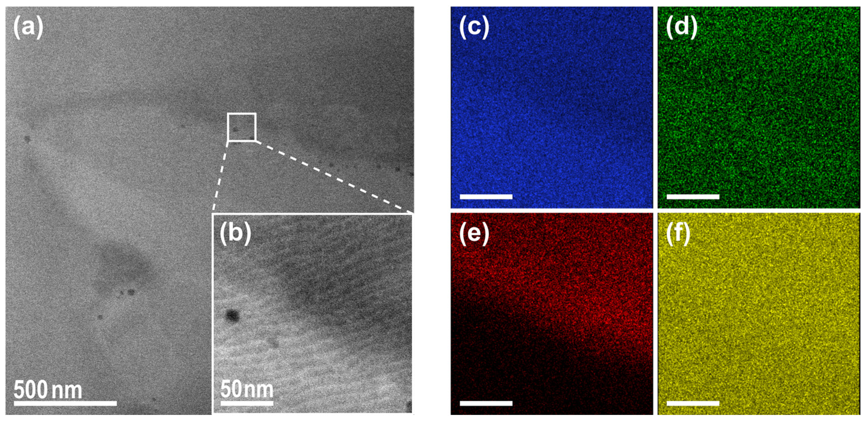
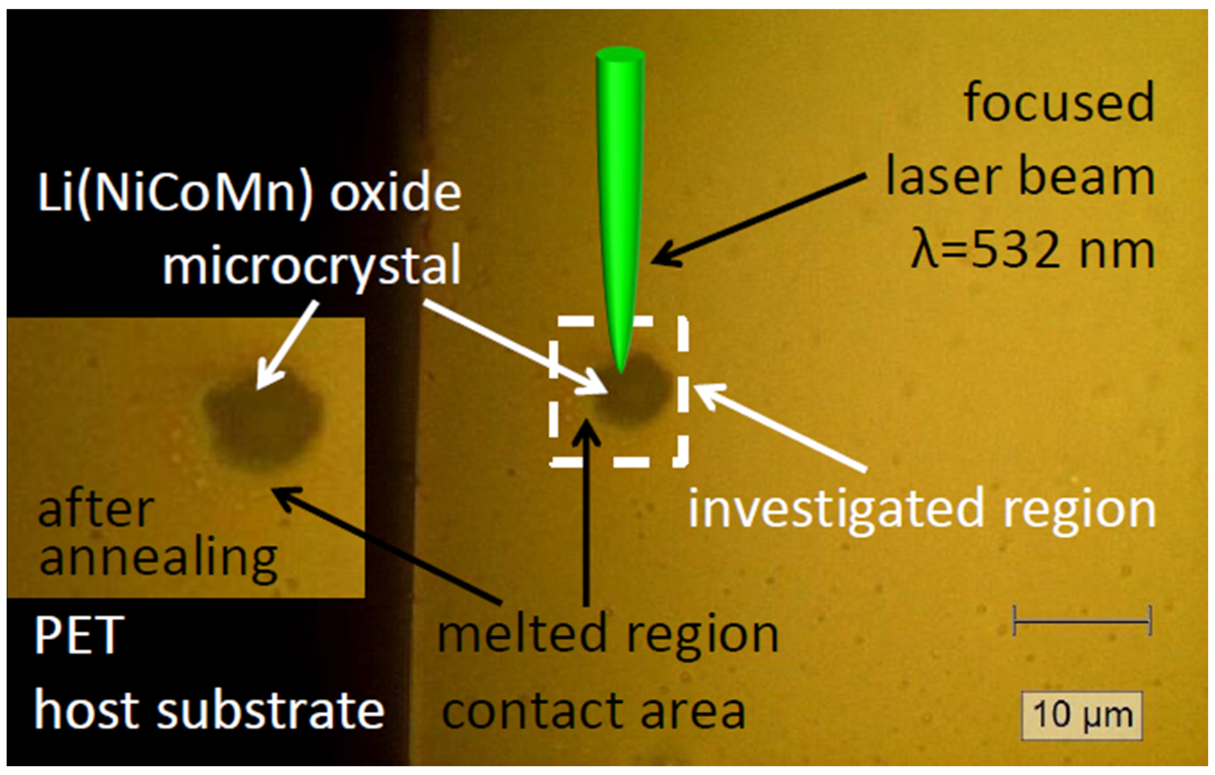
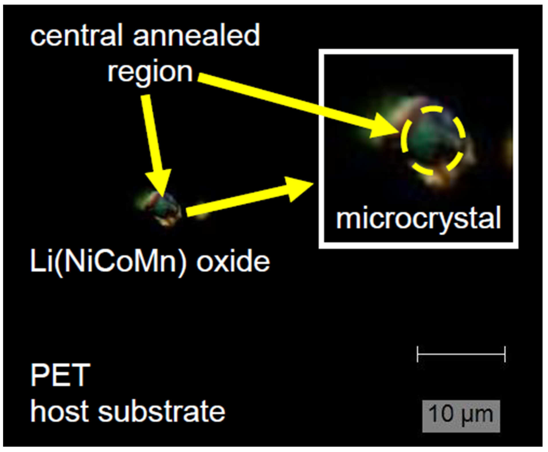
3. Results
4. Conclusions
Author Contributions
Funding
Institutional Review Board Statement
Informed Consent Statement
Data Availability Statement
Conflicts of Interest
References
- Jiang, L.Z.; Zhou, M.F.; Liu, X.N.; Qin, Q.Z. CeO2 thin film as a lithium ion-storage material fabricated by pulsed laser deposition. Acta Phys.-Chim. Sin. 1999, 15, 752–756. [Google Scholar]
- Kohler, R.; Smyrek, P.; Ulrich, S.; Bruns, M.; Trouillet, V.; Pfleging, W. Patterning and annealing of nanocrystalline LiCoO2 thin films. J. Optoelectron. Adv. Mater. 2010, 12, 547–552. [Google Scholar]
- Pröll, J.; Kohler, R.; Torge, M.; Ulrich, S.; Ziebert, C.; Bruns, M.; Seifert, H.J.; Pfleging, W. Laser microstructuring and annealing processes for lithium manganese oxide cathodes. Appl. Surf. Sci. 2011, 257, 9968–9976. [Google Scholar] [CrossRef]
- Kohler, R.; Besser, H.; Hagen, M.; Ye, J.; Ziebert, C.; Ulrich, S.; Proell, J.; Pfleging, W. Laser micro-structuring of magnetron-sputtered SnOx thin films as anode material for lithium ion batteries. Microsyst. Technol. 2011, 17, 225–232. [Google Scholar] [CrossRef]
- Kim, H. Laser-Printed and Processed LiCoO2 CathodeThick Films for Li-Ion Microbatteries. J. Laser Micro/Nanoeng. 2012, 7, 320–325. [Google Scholar] [CrossRef]
- Pröll, J.; Weidler, P.G.; Kohler, R.; Mangang, A.; Heißler, S.; Seifert, H.J.; Pfleging, W. Comparative studies of laser annealing technique and furnace annealing by X-ray diffraction and Raman analysis of lithium manganese oxide thin films for lithium-ion batteries. Thin Solid Film. 2013, 531, 160–171. [Google Scholar] [CrossRef]
- Kirchhoff, M. Laser applications in battery production—From cutting foils to welding the case 2013. In Proceedings of the 2013, 3rd International Electric Drives Production Conference (EDPC) (IEEE), Nuremberg, Germany, 29–30 October 2013; pp. 1–3. [Google Scholar]
- Pröll, J.; Kim, H.; Piqué, A.; Seifert, H.J.; Pfleging, W. Laser-printing and femtosecond-laser structuring of LiMn2O4 composite cathodes for Li-ion microbatteries. J. Power Source 2014, 255, 116–124. [Google Scholar] [CrossRef]
- Schmidt, P.A.; Schmitz, P.; Zaeh, M.F. Laser beam welding of electrical contacts for the application in stationary energy storage devices. J. Laser Appl. 2016, 28, 022423. [Google Scholar] [CrossRef]
- Lutey AH, A.; Fortunato, A.; Carmignato, S.; Fiorini, M. High speed pulsed laser cutting of LiCoO2 Li-ion battery electrodes. Opt. Laser Technol. 2017, 94, 90–96. [Google Scholar] [CrossRef]
- Habedank, J.B.; Endres, J.; Schmitz, P.; Zaeh, M.F.; Huber, H.P. Femtosecond laser structuring of graphite anodes for improved lithium-ion batteries: Ablation characteristics and process design. J. Laser Appl. 2018, 30, 032205. [Google Scholar] [CrossRef]
- Lee, D.; Oh, B.; Suk, J. The Effect of Compactness on Laser Cutting of Cathode for Lithium-Ion Batteries Using Continuous Fiber Laser. Appl. Sci. 2019, 9, 205. [Google Scholar] [CrossRef]
- Lee, D.; Suk, J. Laser cutting characteristics on uncompressed anode for lithium-ion batteries. Energies 2020, 13, 2630. [Google Scholar] [CrossRef]
- Gebrekiros Berhe, M.; Oh, H.G.; Park, S.-K.; Mondal, M.; Lee, D. Effect of laser-induced groove morphology on the wettability and performance of Lithium-ion batteries. Mater. Des. 2023, 231, 112020. [Google Scholar] [CrossRef]
- Khosla, N.; Narayan, J.; Narayan, R.; Sun, X.-G.; Paranthaman, M.P. Nanosecond Laser Annealing of NMC 811 Cathodes for Enhanced Performance. J. Electrochem. Soc. 2023, 170, 030520. [Google Scholar] [CrossRef]
- Ravesio, E.; Lutey AH, A.; Versaci, D.; Romoli, L.; Bodoardo, S. Nanosecond pulsed laser texturing of Li-ion battery electrode current collectors: Electrochemical characterisation of cathode half-cells. Sustain. Mater. Technol. 2023, 38, e00751. [Google Scholar] [CrossRef]
- Berhe, M.G.; Musse, D.; Oh, H.G.; Park, S.K.; Lee, D. Development of laser structured three-dimensional patterns for improved wettability and performance of electrodes for lithium-ion batteries. Colloids Surf. A Physicochem. Eng. Asp. 2024, 697, 134393. [Google Scholar] [CrossRef]
- Pfleging, W. A review of laser electrode processing for development and manufacturing of lithium-ion batteries. Nanophotonics 2018, 7, 549–573. [Google Scholar] [CrossRef]
- Pfleging, W. Recent progress in laser texturing of battery materials: A review of tuning electrochemical performances, related material development, and prospects for large-scale manufacturing. Int. J. Extrem. Manuf. 2021, 3, 012002. [Google Scholar] [CrossRef]
- Hausbrand, R.; Cherkashinin, G.; Ehrenberg, H.; Gröting, M.; Albe, K.; Hess, C.; Jaegermann, W. Fundamental degradation mechanisms of layered oxide Li-ion battery cathode materials: Methodology, insights and novel approaches. Mater. Sci. Eng. B 2015, 192, 3–25. [Google Scholar] [CrossRef]
- Song, Y.; Cui, Y.; Li, B.; Geng, L.; Yan, J.; Zhu, D.; Zhou, P.; Zhou, J.; Yan, Z.; Xue, Q.; et al. Revealing the origin of high-thermal-stability of single-crystal Ni-rich cathodes toward higher-safety batteries. Nano Energy 2023, 116, 108846. [Google Scholar] [CrossRef]
- Finegan, D.P.; Scheel, M.; Robinson, J.B.; Tjaden, B.; Hunt, I.; Mason, T.J.; Millichamp, J.; Di Michiel, M.; Offer, G.J.; Hinds, G.; et al. In-operando high-speed tomography of lithium-ion batteries during thermal runaway. Nat. Commun. 2015, 6, 6924. [Google Scholar] [CrossRef] [PubMed]
- Smyrek, P.; Pfleging, W. Laser materials processing in manufacturing of lithium-ion batteries. In Processing and Manufacturing of Electrodes for Lithium-Ion Batteries; Institution of Engineering and Technology: Stevenage, UK, 2023; pp. 101–127. [Google Scholar]
- Ehrhart, P. Investigation of radiation damage by X-ray diffraction. J. Nucl. Mater. 1994, 216, 170–198. [Google Scholar] [CrossRef]
- Wood, K.N.; Teeter, G. XPS on Li-Battery-Related Compounds: Analysis of Inorganic SEI Phases and a Methodology for Charge Correction. ACS Appl. Energy Mater. 2018, 1, 4493–4504. [Google Scholar] [CrossRef]
- Huang, R.; Ikuhara, Y. STEM characterization for lithium-ion battery cathode materials. Curr. Opin. Solid State Mater. Sci. 2012, 16, 31–38. [Google Scholar] [CrossRef]
- Meddings, N.; Heinrich, M.; Overney, F.; Lee, J.-S.; Ruiz, V.; Napolitano, E.; Seitz, S.; Hinds, G.; Raccichini, R.; Gaberšček, M.; et al. Application of electrochemical impedance spectroscopy to commercial Li-ion cells: A review. J. Power Source 2020, 480, 228742. [Google Scholar] [CrossRef]
- Yamakawa, N.; Jiang, M.; Key, B.; Grey, C.P. Identifying the Local Structures Formed during Lithiation of the Conversion Material, Iron Fluoride, in a Li Ion Battery: A Solid-State NMR, X-ray Diffraction, and Pair Distribution Function Analysis Study. J. Am. Chem. Soc. 2009, 131, 10525–10536. [Google Scholar] [CrossRef]
- Lanz, M.; Lehmann, E.; Imhof, R.; Exnar, I.; Novák, P. In situ neutron radiography of lithium-ion batteries during charge/discharge cycling. J. Power Source 2001, 101, 177–181. [Google Scholar] [CrossRef]
- Heber, M.; Hofmann, K.; Hess, C. Raman Diagnostics of Cathode Materials for Li-Ion Batteries Using Multi-Wavelength Excitation. Batteries 2022, 8, 10. [Google Scholar] [CrossRef]
- Flores, E.; Novák, P.; Aschauer, U.; Berg, E.J. Cation Ordering and Redox Chemistry of Layered Ni-Rich Ni-Rich LixNi1–2yCoyMnO2: An Operando Raman Spectroscopy Study. Chem. Mater. 2020, 32, 186–194. [Google Scholar] [CrossRef]
- Zhang, B.; Tekle, H.; O’Malley, R.J.; Sander, T.; Smith, J.D.; Gerald, R.E.; Huang, J. In Situ and Real-Time Mold Flux Analysis Using a High-Temperature Fiber-Optic Raman Sensor for Steel Manufacturing Applications. J. Light. Technol. 2023, 41, 4419–4429. [Google Scholar] [CrossRef]
- Ferreira, A.N.C.; Ferreira, W.C.; Duarte, A.V.; Santos, C.C.; Freire, P.T.C.; Luz-Lima, C.; Moura, J.V.B. In situ high-temperature Raman scattering study of monoclinic Ag2Mo2O7 microrods. Spectrochim. Acta Part A Mol. Biomol. Spectrosc. 2023, 295, 122632. [Google Scholar] [CrossRef] [PubMed]
- Zhang, B.; Tekle, H.; O’Malley, R.J.; Smith, J.D.; Gerald, R.E.; Huang, J. In Situ High-Temperature Raman Spectroscopy via a Remote Fiber-Optic Raman Probe. IEEE Trans. Instrum. Meas. 2023, 72, 1–8. [Google Scholar] [CrossRef]
- Branch, S.D.; Felmy, H.M.; Schafer Medina, A.; Bryan, S.A.; Lines, A.M. Exploring the Complex Chemistry of Uranium within Molten Chloride Salts. Ind. Eng. Chem. Res. 2023, 62, 14901–14909. [Google Scholar] [CrossRef]
- Templier, F. GaN-based emissive microdisplays: A very promising technology for compact, ultra-high brightness display systems. J. Soc. Inf. Disp. 2016, 24, 669–675. [Google Scholar] [CrossRef]
- Mikulics, M.; Arango, Y.C.; Winden, A.; Adam, R.; Hardtdegen, A.; Grützmacher, D.; Plinski, E.; Gregušová, D.; Novák, J.; Kordoš, P.; et al. Direct electro-optical pumping for hybrid CdSe nanocrystal/III-nitride based nano-light-emitting diodes. Appl. Phys. Lett. 2016, 108, 061107. [Google Scholar] [CrossRef]
- Ra, Y.-H.; Wang, R.; Woo, S.Y.; Djavid, M.; Sadaf, S.M.; Lee, J.; Botton, G.A.; Mi, Z. Full-Color Single Nanowire Pixels for Projection Displays. Nano Lett. 2016, 16, 4608–4615. [Google Scholar] [CrossRef] [PubMed]
- Krause, T.; Hanke, M.; Nicolai, L.; Cheng, Z.; Niehle, M.; Trampert, A.; Kahnt, M.; Falkenberg, G.; Schroer, C.G.; Hartmann, J.; et al. Structure and Composition of Isolated Core-Shell (In,Ga)N/GaN Rods Based on Nanofocus X-Ray Diffraction and Scanning Transmission Electron Microscopy. Phys. Rev. Appl. 2017, 7, 024033. [Google Scholar] [CrossRef]
- Wierer, J.J.; Tansu, N. III-Nitride Micro-LEDs for Efficient Emissive Displays. Laser Photon. Rev. 2019, 13, 1900141. [Google Scholar] [CrossRef]
- Franch, N.; Canals, J.; Moro, V.; Alonso, O.; Moreno, S.; Vilà, A.; Prades, J.D.; Gülink, J.; Wasisto, H.S.; Waag, A.; et al. Towards a super-resolution structured illumination microscope based on an array of nanoLEDs. In Novel Optical Systems, Methods, and Applications XXII; Hahlweg, C.F., Mulley, J.R., Eds.; SPIE: Bellingham, DC, USA, 2019; p. 23. [Google Scholar]
- Ding, K.; Avrutin, V.; Izyumskaya, N.; Özgür, Ü.; Morkoç, H. Micro-LEDs, a Manufacturability Perspective. Appl. Sci. 2019, 9, 1206. [Google Scholar] [CrossRef]
- Mikulics, M.; Hardtdegen, H.H. Fully photon operated transmistor/all-optical switch based on a layered Ge1Sb2Te4 phase change medium. FlatChem 2020, 23, 100186. [Google Scholar] [CrossRef]
- Mikulics, M.; Sofer, Z.; Winden, A.; Trellenkamp, S.; Förster, B.; Mayer, J.; Hardtdegen, H.H. Nano-LED induced chemical reactions for structuring processes. Nanoscale Adv. 2020, 2, 5421–5427. [Google Scholar] [CrossRef]
- Kishino, K.; Sakakibara, N.; Narita, K.; Oto, T. Two-dimensional multicolor (RGBY) integrated nanocolumn micro-LEDs as a fundamental technology of micro-LED display. Appl. Phys. Express 2020, 13, 014003. [Google Scholar] [CrossRef]
- Zhou, G.; Lin, R.; Qian, Z.; Zhou, X.; Shan, X.; Cui, X.; Tian, P. GaN-based micro-LEDs and detectors defined by current spreading layer: Size-dependent characteristics and their multifunctional applications. J. Phys. D. Appl. Phys. 2021, 54, 335104. [Google Scholar] [CrossRef]
- Wu, M.-C.; Chen, I.-T. High-Resolution 960 × 540 and 1920 × 1080 UV Micro Light-Emitting Diode Displays with the Application of Maskless Photolithography. Adv. Photonics Res. 2021, 2, 1–8. [Google Scholar] [CrossRef]
- Mikulics, M.; Mayer, J.; Hardtdegen, H.H. Cutting-edge nano-LED technology. J. Appl. Phys. 2022, 131, 110903. [Google Scholar] [CrossRef]
- Mikulics, M.; Adam, R.; Sobolewski, R.; Heidtfeld, S.; Cao, D.; Bürgler, D.E.; Schneider, C.M.; Mayer, J.; Hardtdegen, H.H. Nano-LED driven phase change evolution of layered chalcogenides for Raman spectroscopy investigations. FlatChem 2022, 36, 100447. [Google Scholar] [CrossRef]
- Chen, D.; Chen, Y.-C.; Zeng, G.; Zhang, D.W.; Lu, H.-L. Integration Technology of Micro-LED for Next-Generation Display. Research 2023, 6, 47. [Google Scholar] [CrossRef]
- Mikulics, M.; Kordoš, P.; Gregušová, D.; Sofer, Z.; Winden, A.; Trellenkamp, S.; Moers, J.; Mayer, J.; Hardtdegen, H. Conditioning nano-LEDs in arrays by laser-micro-annealing: The key to their performance improvement. Appl. Phys. Lett. 2021, 118, 043101. [Google Scholar] [CrossRef]
- Ruess, R.; Ulherr, M.A.; Trevisanello, E.; Schröder, S.; Henss, A.; Janek, J. Transition Metal Oxides and Li2CO3 as Precursors for the Synthesis of Ni-Rich Single-Crystalline NCM for Sustainable Lithium-Ion Battery Production. J. Electrochem. Soc. 2022, 169, 070531. [Google Scholar] [CrossRef]
- Gardner, B.; Matousek, P.; Stone, N. Direct monitoring of light mediated hyperthermia induced within mammalian tissues using surface enhanced spatially offset Raman spectroscopy (T-SESORS). Analyst 2019, 144, 3552–3555. [Google Scholar] [CrossRef]
- Bowie, B.T.; Griffiths, P.R. Determination of the Resolution of a Multichannel Raman Spectrometer Using Fourier Transform Raman Spectra. Appl. Spectrosc. 2003, 57, 190–196. [Google Scholar] [CrossRef] [PubMed]
- Brooker, M.H.; Bates, J.B. Raman and Infrared Spectral Studies of Anhydrous Li2CO3 and Na2CO3. J. Chem. Phys. 1971, 54, 4788–4796. [Google Scholar] [CrossRef]
- Hase, Y.; Yoshida IV, P. Low frequency bands of Li2CO3 crystal. Spectrochim. Acta Part. A Mol. Spectrosc. 1979, 35, 379. [Google Scholar] [CrossRef]
- Brooker, M.H.; Wang, J. Raman and infrared studies of lithium and cesium carbonates. Spectrochim. Acta Part. A Mol. Spectrosc. 1992, 48, 999–1008. [Google Scholar] [CrossRef]
- Pasierb, P.; Komornicki, S.; Rokita, M.; Rȩkas, M. Structural properties of Li2CO3–BaCO3 system derived from IR and Raman spectroscopy. J. Mol. Struct. 2001, 596, 151–156. [Google Scholar] [CrossRef]
- Kerlau, M.; Marcinek, M.; Srinivasan, V.; Kostecki, R.M. Studies of local degradation phenomena in composite cathodes for lithium-ion batteries. Electrochim. Acta 2007, 52, 5422–5429. [Google Scholar] [CrossRef]
- Zhang, X.; Mauger, A.; Lu, Q.; Groult, H.; Perrigaud, L.; Gendron, F.; Julien, C.M. Synthesis and characterization of LiNi1/3Mn1/3Co1/3O2 by wet-chemical method. Electrochim. Acta 2010, 55, 6440–6449. [Google Scholar] [CrossRef]
- Zhao, H.; Bai, Y.; Jin, H.; Zhou, J.; Wang, X.; Wu, C. Unveiling thermal decomposition kinetics of Single-Crystalline Ni-Rich LiNi0.88Co0.07Mn0.05O2 cathode for safe Lithium-Ion batteries. Chem. Eng. J. 2022, 435, 134927. [Google Scholar] [CrossRef]
- Ruther, R.E.; Callender, A.F.; Zhou, H.; Martha, S.K.; Nanda, J. Raman Microscopy of Lithium-Manganese-Rich Transition Metal Oxide Cathodes. J. Electrochem. Soc. 2015, 162, A98–A102. [Google Scholar] [CrossRef]
- Kim, A.-Y.; Strauss, F.; Bartsch, T.; Teo, J.H.; Hatsukade, T.; Mazilkin, A.; Janek, J.; Hartmann, P.; Brezesinski, T. Stabilizing Effect of a Hybrid Surface Coating on a Ni-Rich NCM Cathode Material in All-Solid-State Batteries. Chem. Mater. 2019, 31, 9664–9672. [Google Scholar] [CrossRef]
- Mikulics, M.; Hardtdegen, H.; Adam, R.; Grützmacher, D.; Gregušová, D.; Novák, J.; Kordoš, P.; Sofer, Z.; Serafini, J.; Zhang, J.; et al. Impact of thermal annealing on nonequilibrium carrier dynamics in single-crystal, freestanding GaAs mesostructures. Semicond. Sci. Technol. 2014, 29, 045022. [Google Scholar] [CrossRef]
- Mikulics, M.; Lu, J.G.; Huang, L.; Tse, P.L.; Zhang, J.Z.; Mayer, J.; Hardtdegen, H. Laser micro annealing conditioning for the suppression of statistical scatter in freestanding Sb2Te3 nanowire resistance. FlatChem 2020, 21, 100164. [Google Scholar] [CrossRef]
- Conde, J.P.; Alpuim, P.; Chu, V. Thin-Film Transistors on PET at 100 °C. MRS Proc. 2002, 715, A3.1. [Google Scholar] [CrossRef]
- Paetzold, R.; Heuser, K.; Henseler, D.; Roeger, S.; Wittmann, G.; Winnacker, A. Performance of flexible polymeric light-emitting diodes under bending conditions. Appl. Phys. Lett. 2003, 82, 3342–3344. [Google Scholar] [CrossRef]
- Chwang, A.B.; Rothman, M.A.; Mao, S.Y.; Hewitt, R.H.; Weaver, M.S.; Silvernail, J.A.; Rajan, K.; Hack, M.; Brown, J.J.; Chu, X.; et al. Thin film encapsulated flexible organic electroluminescent displays. Appl. Phys. Lett. 2003, 83, 413–415. [Google Scholar] [CrossRef]
- Ichikawa, Y.; Yoshida, T.; Hama, T.; Sakai, H.; Harashima, K. Production technology for amorphous silicon-based flexible solar cells. Sol. Energy Mater. Sol. Cells 2001, 66, 107–115. [Google Scholar] [CrossRef]
- Jinhua, L.; Ningyi, Y.; Chan HL, W. Preparation of PCLT/P(VDF-TrFE) pyroelectric sensor based on plastic film substrate. Sens. Actuators A Phys. 2002, 100, 231–235. [Google Scholar] [CrossRef]
- Mikulics, M.; Adam, R.; Marso, M.; Forster, A.; Kordos, P.; Luth, H.; Wu, S.; Zheng, X.; Sobolewski, R. Ultrafast low-temperature-grown epitaxial GaAs photodetectors transferred on flexible plastic substrates. IEEE Photonics Technol. Lett. 2005, 17, 1725–1727. [Google Scholar] [CrossRef]
- Jia, H.; Veldeman, J.; Burgelman, M. Magnetic properties and microstructure of CoCr and CoCrTa thin films sputtered at high pressure on a PET substrate. J. Magn. Magn. Mater. 2001, 223, 73–80. [Google Scholar] [CrossRef]
- Jung, R.; Morasch, R.; Karayaylali, P.; Phillips, K.; Maglia, F.; Stinner, C.; Shao-Horn, Y.; Gasteiger, H.A. Effect of Ambient Storage on the Degradation of Ni-Rich Positive Electrode Materials (NMC811) for Li-Ion Batteries. J. Electrochem. Soc. 2018, 165, A132–A141. [Google Scholar] [CrossRef]
- Terlemezoglu, M.; Surucu, O.; Isik, M.; Gasanly, N.M.; Parlak, M. Temperature-dependent optical characteristics of sputtered NiO thin films. Appl. Phys. A 2022, 128, 50. [Google Scholar] [CrossRef]

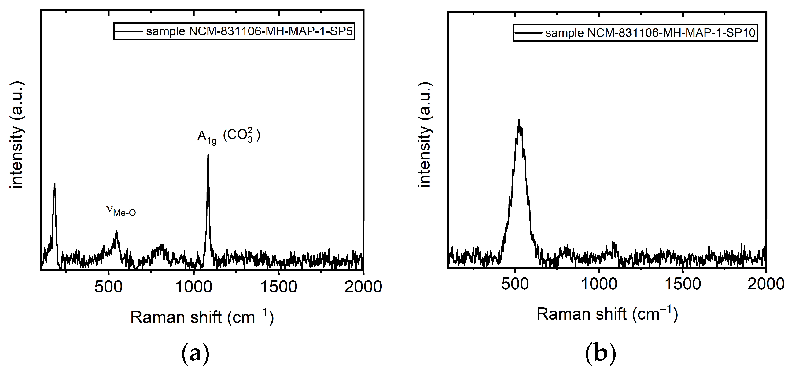
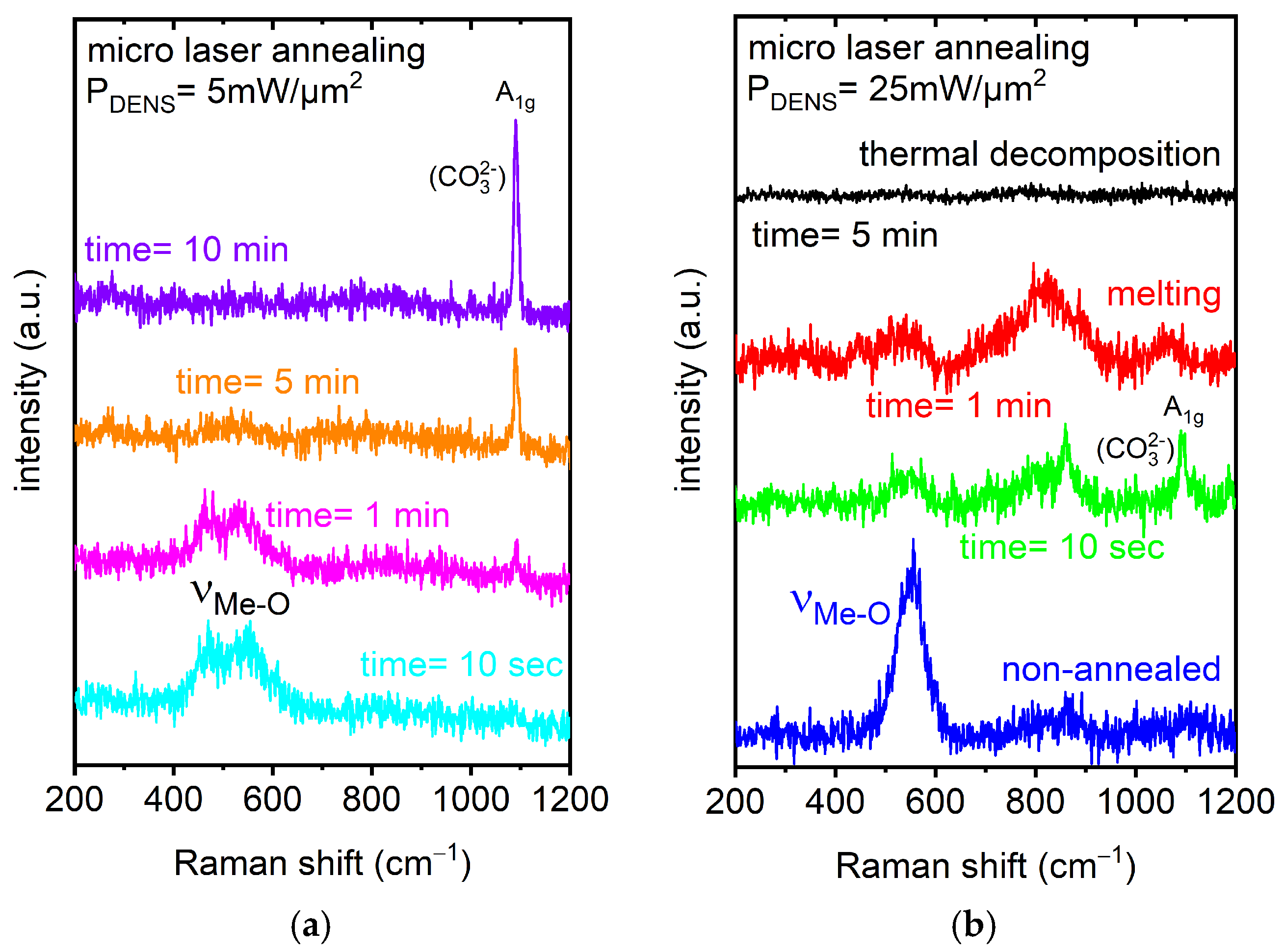
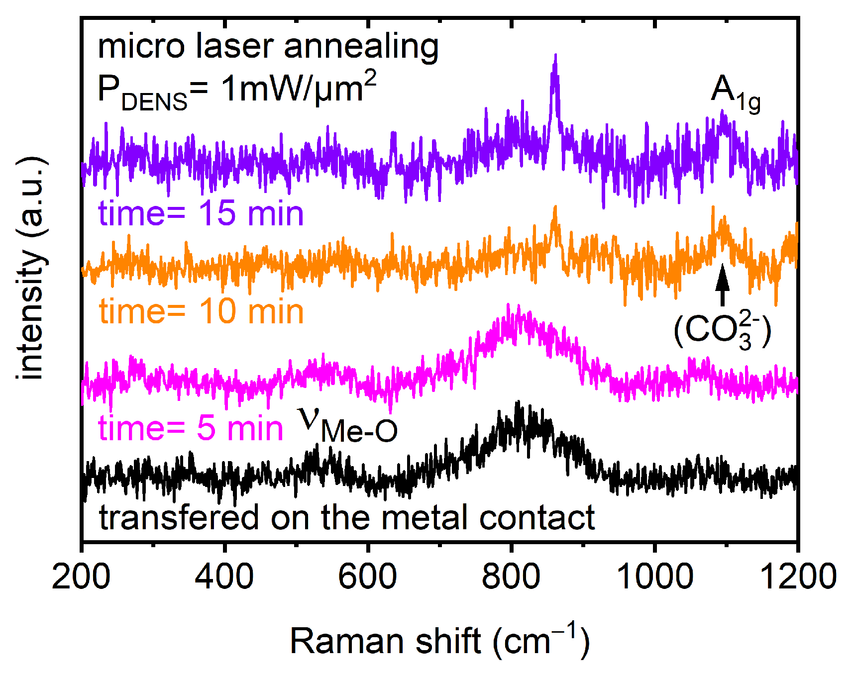
| Optical Power Density (mW/µm2) | Annealing Time | Raman RT Study 200–1200 (cm−1) | Notice | Interpretation | |
|---|---|---|---|---|---|
| Mode | Assignment | ||||
| pristine | pristine | 550 | νMe-O | broad band FWHM ~70cm−1 | overlapping Me-O stretching and bending vibrations related to Ni, Co, and Mn as the metal (Me) [59,60] |
| 5 | 10 s | 470 | Eg | overlapping O-Me-O bending vibrations related to Ni, Co, and Mn as the metal (Me) [59,60] | |
| 550 | A1g | overlapping Me-O symmetric stretching vibrations related to Ni, Co, and Mn as the metal (Me) [59,60] | |||
| 1 min | 470 | Eg | the intensity began to decrease | ||
| 550 | A1g | the intensity began to decrease | |||
| 1085 | A1g | appeared | CO32− symmetric stretching vibrations [55,57,58] | ||
| 5 min | 470, 550 | Eg and A1g | both bands: the intensity dramatically decreased | beginning phase transition | |
| 1085 | A1g | intensity increase | |||
| 10 min | 1085 | A1g | intensity increase | recrystallization | |
| 25 | 10 s | 520–580 | several overlapping modes detected | ||
| 860 | 2TO | intensity increase | Ni oxide-related [74] | ||
| 1085 | A1g | intensity decrease | CO32− symmetric stretching vibrations [55,57,58] | ||
| 1 min | 520–580 | several overlapping modes detected | |||
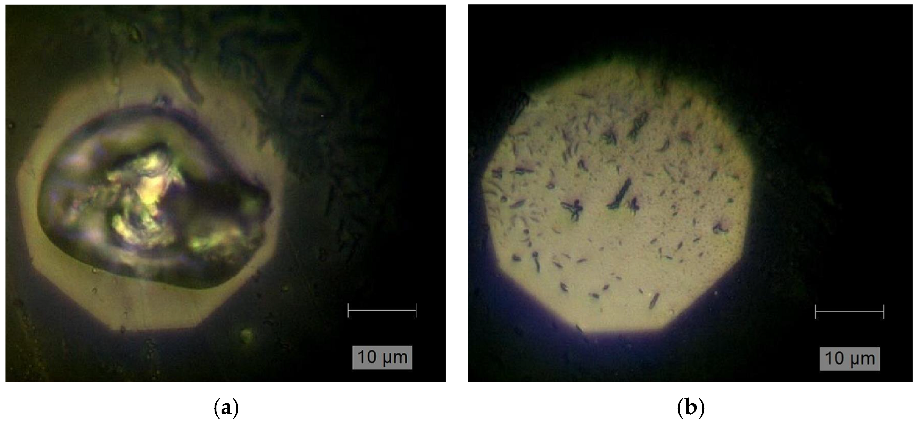
| 770–890 | several overlapping modes detected | Ni oxide-related [74] melting process confirmed by optical inspection | |||
| 1050–1090 | A1g | the intensity began to dramatically decrease | |||
| 5 min | bands not detected anymore | thermal decomposition | |||
Disclaimer/Publisher’s Note: The statements, opinions and data contained in all publications are solely those of the individual author(s) and contributor(s) and not of MDPI and/or the editor(s). MDPI and/or the editor(s) disclaim responsibility for any injury to people or property resulting from any ideas, methods, instructions or products referred to in the content. |
© 2025 by the authors. Licensee MDPI, Basel, Switzerland. This article is an open access article distributed under the terms and conditions of the Creative Commons Attribution (CC BY) license (https://creativecommons.org/licenses/by/4.0/).
Share and Cite
Ahrens, L.; Mikulics, M.; Schröder, S.; Mayer, J.; Hardtdegen, H.H. Laser-Micro-Annealing of Microcrystalline Ni-Rich NCM Oxide: Towards Micro-Cathodes Integrated on Polyethylene Terephthalate Flexible Substrates. Materials 2025, 18, 680. https://doi.org/10.3390/ma18030680
Ahrens L, Mikulics M, Schröder S, Mayer J, Hardtdegen HH. Laser-Micro-Annealing of Microcrystalline Ni-Rich NCM Oxide: Towards Micro-Cathodes Integrated on Polyethylene Terephthalate Flexible Substrates. Materials. 2025; 18(3):680. https://doi.org/10.3390/ma18030680
Chicago/Turabian StyleAhrens, Lara, Martin Mikulics, Steffen Schröder, Joachim Mayer, and Hilde Helen Hardtdegen. 2025. "Laser-Micro-Annealing of Microcrystalline Ni-Rich NCM Oxide: Towards Micro-Cathodes Integrated on Polyethylene Terephthalate Flexible Substrates" Materials 18, no. 3: 680. https://doi.org/10.3390/ma18030680
APA StyleAhrens, L., Mikulics, M., Schröder, S., Mayer, J., & Hardtdegen, H. H. (2025). Laser-Micro-Annealing of Microcrystalline Ni-Rich NCM Oxide: Towards Micro-Cathodes Integrated on Polyethylene Terephthalate Flexible Substrates. Materials, 18(3), 680. https://doi.org/10.3390/ma18030680