Article

First-Principles Understanding of Mono- and Dual-Emissions in AZnOS:Bi3+ (A = Ba, Ca) Phosphors

1
College of Electronic and Optical Engineering & College of Flexible Electronics (Future Technology), Nanjing University of Posts & Telecommunications, Nanjing 210023, China
2
School of Optoelectronic Engineering, Chongqing University of Posts and Telecommunications, Chongqing 400065, China
3
Centre of Excellence for Photoconversion, Vinča Institute of Nuclear Sciences—National Institute of the Republic of Serbia, University of Belgrade, 11000 Belgrade, Serbia
4
Institute of Physics, University of Tartu, W. Ostwald Str. 1, 50411 Tartu, Estonia
5
Faculty of Science and Technology, Jan Długosz University, Armii Krajowej 13/15, PL-42200 Częstochowa, Poland
6
Academy of Romanian Scientists, Ilfov Str. No. 3, 050044 Bucharest, Romania
*
Authors to whom correspondence should be addressed.
Materials 2025, 18(3), 657; https://doi.org/10.3390/ma18030657
Submission received: 18 December 2024 / Revised: 22 January 2025 / Accepted: 24 January 2025 / Published: 2 February 2025
(This article belongs to the Section Materials Simulation and Design)

Abstract

:
The AZnOS:Bi3+ (A = Ba, Ca) phosphors exhibit mono- and dual-emission phenomena based on the different choices of cation, making them an ideal prototype for dual-emission mechanism studies of Bi3+ ions. Here, first-principles calculations were performed to investigate the site occupancy, defect levels, and luminescence properties of the AZnOS:Bi3+ systems. The formation energy calculations show that the bismuth dopants are mainly in the trivalent charge state, with the Bi3+ ions preferring the Ca sites in CaZnOS but the Zn sites in BaZnOS. Such cation-selective occupancy mainly results in the difference between the mono- and dual-emission phenomena in the two hosts. The excitation and emission energies predicted by calculations are in good agreement with the measurements. Our calculations show that the lowest excited state 3P0,1 provides the dominant emission in both CaZnOS:Bi3+ and BaZnOS:Bi3+ phosphors. In light of the experimental and theoretical results, the metastable excited state of Bi2+ + hVBM (hole at the valence band maximum) is the origin of the additional emission bands in BaZnOS:Bi3+. These results provide the basis of emission band tuning and novel material design for Bi3+-doped phosphors.

1. Introduction

In contrast to the general mono-emission phenomenon, some single Bi3+-doped phosphors exhibit dual-emission bands, e.g., Y2O3:Bi3+ [1], MgGa2O4:Bi3+ [2]. They provide an extra red-shifted emission band in addition to the commonly observed green or blue emission band. Recently, such dual-emission character has become attractive due to the potential application in anti-counterfeiting [3], temperature sensing [4], and healthcare lighting [5], where Bi3+ ions, as an important activator, can help to control the trapping and detrapping processes through valence or conduction band engineering, endowing the host matrix with multifunctional phosphorescent performances. Bi3+-activated dual-emission materials with a wide spectral response range can effectively promote the effective dynamic anti-counterfeiting properties. Understanding the dual-emission mechanisms of Bi3+ dopants is crucially important to improve the luminescence performance and expand the application boundaries of the Bi3+-doped phosphors. On the one hand, the spectral assignment and the origin of the emission bands should be clarified. On the other hand, the schemes for tuning mono-emitting phosphors into dual-emitting ones should be explored. However, the complex optical transitions of Bi3+-doped phosphors (except for the 1S03P0,1 transition between two electron configurations of a Bi3+ ion, in which there are excitation and emission processes involving charge transfer between a Bi3+ ion and the host, such as the valence band to Bi3+ charge transfer, usually denoted as CT, and the ionization of an electron from Bi3+ to the condition band, usually denoted as metal–metal charge transfer (MMCT)) always bring challenges in the spectral assignment and the luminescence studies. Several potential dual-emission mechanisms have been proposed, including the site-selective occupancy of dopants [6], influence of bismuth ions with lower valence states [7], formation of Bi pairs or clusters [8], and Jahn–Teller distortion of the local environment [9]. It is difficult to obtain an explicit understanding of dual-emission mechanisms using experimental methods alone.
The AZnOS (A = Ca, Ba) crystals are promising hosts that exhibit excellent piezoelectric and luminescent properties, and the different cations at the A site are responsible for the mono- and dual-emission phenomena. Under 366 nm excitation, Bi-doped CaZnOS and BaZnOS show strong broad emission bands with their peaks at about 485 and 507 nm, respectively, but an extra broad emission band with the peak at 627 nm was only observed in BaZnOS:Bi under 297 nm excitation [10]. The experimental studies indicated that the A sites are the most suitable and stable sites for the Bi ions to occupy according to the Rietveld refinement, and the dopant Bi ions were found to be in the trivalent state in CaZnOS. For the Bi dopants in BaZnOS, the divalent and trivalent charge states coexist. The dual-emission was attributed to bismuth dopants with different charge states. However, such an explanation faced inconsistencies with the excitation spectra and the decay time properties, e.g., the decay time of 627 nm emission (884 ns) in BaZnOS:Bi3+ is close to the emission peak at 485 nm (773 ns) in CaZnOS:Bi3+ [10]. And similar dual-emissions were observed in Sb3+-doped CaZnOS [11]. In addition to the luminescence properties, the piezoelectric properties of Bi3+-doped AZnOS have also attracted great interest. It exhibits intense mechanoluminescence in the visible light region with potential applications in pressure sensing [12,13] and stress-based anti-counterfeiting technologies [14]. A systematic investigation of the electronic structures and luminescence mechanisms of Bi3+-doped AZnOS phosphors will provide insights into potential strategies for enhancing performance, as well as the design of novel phosphors with exceptional piezoelectric and luminescent properties. First-principles calculations have been widely used as a powerful tool to investigate and elucidate the excitation, relaxation, and emission processes of a large number of bismuth-doped phosphors [15]. Previous theoretical studies on AZnOS:Bi3+ (A = Ca, Ba) systems focused on the ground-state properties of hosts and dopants, e.g., Zhang et al. studied the elastic and tensile properties [16] and Pan et al. studied the site occupancy of bismuth by the binding energy comparison [10]. However, these studies lack the excited-state properties that are essential for the investigation of the dynamic emission processes.
Herein, first-principles calculations were employed to study the luminescence properties of bismuth in the oxysulfide AZnOS (A = Ca, Ba), in particular, the dual-emission mechanism of BaZnOS:Bi3+. The local environments of the dopants and the formation energies of the defects in AZnOS:Bi3+ systems were studied to clarify the site occupancy and the valence state of the bismuth dopants. The defect levels and the electronic structures were studied to obtain the optical luminescence properties of the Bi3+ ions in the two hosts and to reveal the origin of the dual-emission bands. The emission properties of the lower-charge-state bismuth ions (Bi2+ and Bi+) were also discussed in order to clarify the hypothesis. Our studies on the mono- and dual-emission mechanisms of AZnOS:Bi3+ systems can assist in the novel material design and the emission adjustment, thereby expanding the potential applications of Bi3+-doped phosphors, such as achieving high-quality white light by controlling the relative intensities of the mono- and dual-emission peaks.

2. Materials and Methods

In our calculation, the geometric structure relaxations were performed in the Strongly Constrained and Appropriately Normed (SCAN) functional [17] within the VASP code [18]. Semicore electrons were explicitly treated with the recommended projector augment wave pseudopotentials [19]. Spin–orbit coupling (SOC) was included for bismuth- and antimony-containing supercells. The cutoff energy of the plane-wave basis was set to 520 eV, while the convergence criteria were 10 5 eV for electronic energy minimization and 0.02 eV/Å for Hellman–Feynman forces on each atom. Based on the relaxed equilibrium geometric structures, the PBE0 functional [20] with 25% Hartree–Fock exchange was used in obtaining better electronic structure and photoluminescence properties. The defects containing BaZnOS crystals were modeled using a 3 × 1 × 2 supercell, while a supercell with new base vectors of 3 ( a + b ) , 2 ( a b ) , and c was utilized for CaZnOS. The 7 × 7 × 5 (CaZnOS) and 7 × 3 × 5 (BaZnOS) k-point grids were used in sampling the Brillouin zone of the unit cell, while only one k point Γ was used for all the supercells.
The formation energy of a defect X in the charge state of q can be derived as follows [21]:
E f ( X q , E F ) = E t o t X q E t o t b u l k i n i μ i + q E F ,
where E t o t is the total energy of the optimized supercells, n i are the numbers of atoms in elements i that are added to ( n i > 0) and/or removed from ( n i < 0) the perfect supercell, and μ i are the corresponding chemical potentials of these species. The Fermi energy level E F represents the chemical potential of the electrons in the host. The thermodynamic charge transition level ϵ ( q 1 / q 2 ) was utilized to predict the positions of defect levels, and it is defined as the Fermi level where the defect formation energies of X q 1 and X q 2 are equal. It can be derived from
ϵ ( q 1 / q 2 ) = E f X q 1 ,     E f = 0 E f X q 2 ,     E f = 0 q 2 q 1 ,
where post hoc corrections to the total energy of charged defects are applied according to the method proposed in Ref. [22].
For Bi3+ ion-doped systems, the dominant emission can originate from the equilibrium structure of the 6s16p1 (3P0,1) excited state and the charge transfer state, including the MMCT excited state (Bi4+ + e) and the CT excited state (Bi2+ + h). Since an extra extended electron or hole in the energy band of the host hardly influences the ligand environment and luminescent property of the emission center, the equilibrium geometric structures for MMCT and CT excited states were approximately obtained by geometry optimization for the supercell with electron number setting corresponding to Bi4+ and Bi2+ [23,24]. The 3P0,1 excited state was approximated by constraining the electron occupancy to (6s1/2)1(6p1/2)1 for A Z n O S : B i 3 + , where the 6s1/2 and 6p1/2 are Kohn–Sham orbitals obtained with the SCAN + SOC functional. For the optical transition energy calculations, the MMCT excitation energy is approximated by the difference in the energy of the A Z n O S : B i 4 + system plus an electron in CBM from that of the A Z n O S : B i 3 + system. Similarly, the CT absorption and emission energies can be calculated as the difference in the energy of A Z n O S : B i 2 + plus a hole from that of the A Z n O S : B i 3 + system. For optical transitions between 1S0 and 3P0,1, the standard ΔSCF-DFT procedure was employed.

3. Results and Discussion

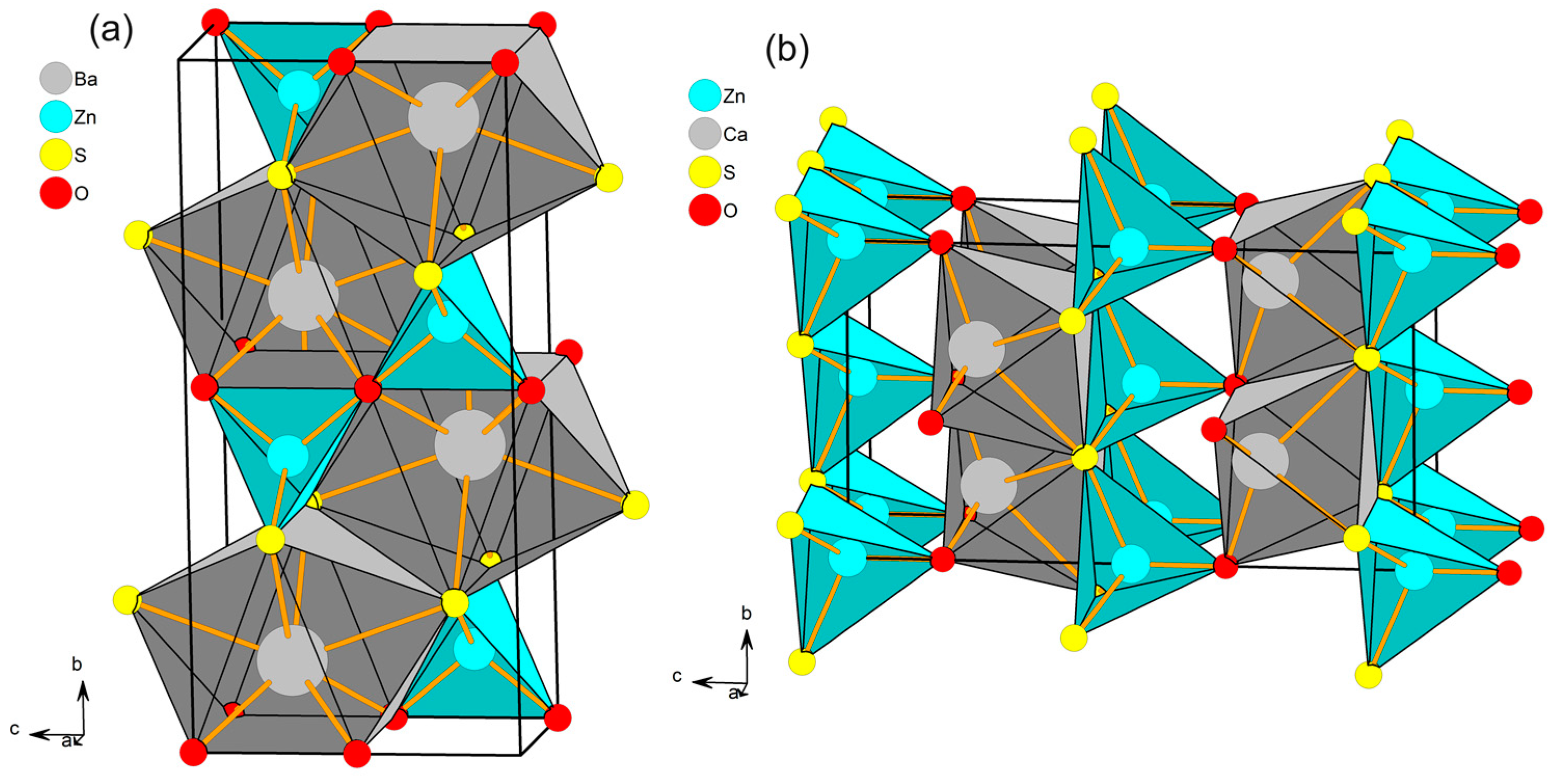
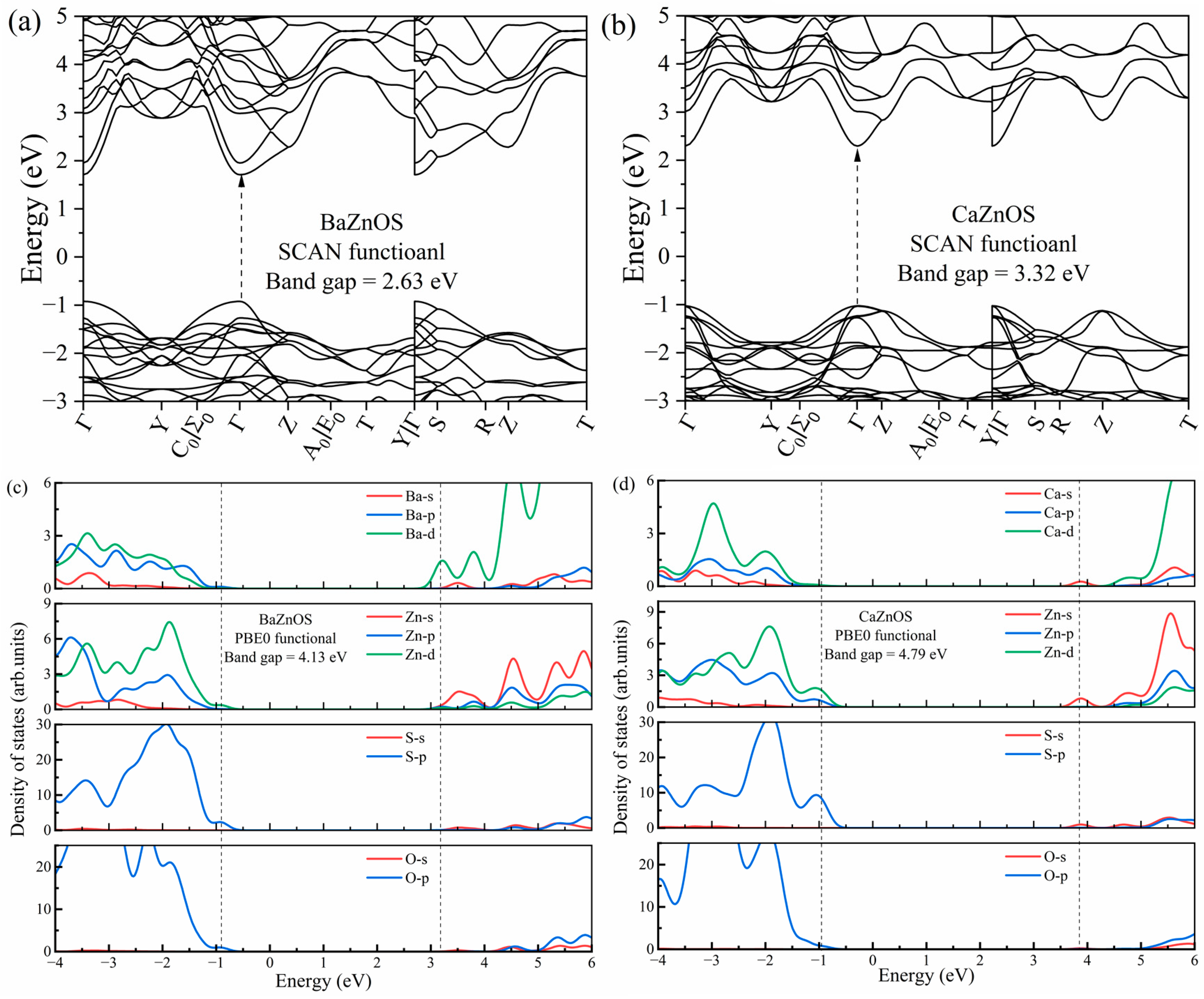
3.1. Geometric and Electronic Structures of Hosts

As shown in Figure 1, the crystal structures of CaZnOS and BaZnOS compounds belong to the hexagonal (P63mc, No. 186) and orthorhombic (Cmcm, No. 63) structures, respectively.
The difference in ionic radii between Ca2+ (1.00 Å, coordination number CN = 6) and Ba2+ (1.35 Å, CN = 6; 1.42 Å, CN = 8) ions has great influence on the local structure of the two hosts. For CaZnOS, all the Ca cations are located at the Wyck 2b sites are surrounded by three oxygen ligands (bond length BL = 2.27 Å) and three sulfur ligands (BL = 3.05 Å). The Zn cations located at the Wyck 2a sites are surrounded by one oxygen ligand (BL = 1.90 Å) and three sulfur ligands (BL = 2.35 Å). However, there are eight ligands for Ba sites located at the Wyck 4c sites in BaZnOS, including four oxygen ligand and four sulfur ligands with bond lengths of 2.86 Å and 3.26 Å, respectively. For the Zn cation in BaZnOS, it is also located at the Wyck 4c sites and is surrounded by two oxygen anions (BL = 1.98 Å) and two sulfur anions (BL = 2.32 Å). Traditionally, the site occupancy of dopants is judged by the ionic radius. Here, the doped Bi3+ ions (1.17 Å, CN = 8; 1.03 Å, CN = 6) more likely occupy the Ca2+ cation sites (1.00 Å, CN = 6) rather than the Zn2+ sites (r = 0.60 Å, CN = 4) for CaZnOS. However, the occupancy of the Bi3+ dopant in BaZnOS remains confusing because the ionic radius of Bi3+ is remarkably mismatched with those of the two cation sites. Previous experimental work has pointed out the difficulty in distinguishing the exact site occupancy of Bi from the XRD patterns [10] and proposed the requirements of the first-principles calculations.
Figure 2 shows the SCAN-calculated band structures of the pristine AZnOS (A = Ca, Ba), where the valence band maximum (VBM) and conduction band minimum (CBM) both locate on the Γ point, implying that both materials are direct gap semiconductors. The Kohn–Sham band gaps calculated with the SCAN functional are 3.32 eV and 2.63 eV for A = Ca and Ba, respectively. The results are better than the values obtained with the Perdew–Burke–Ernzerhof functional (PBE) [25], e.g., 2.81 eV for CaZnOS and 2.27 eV for BaZnOS, while they remain seriously underestimated compared to the experimentally reported optical band gaps. The band gap values are 4.50 eV for CaZnOS and 4.00 eV for BaZnOS, characterized by host absorption spectra and diffuse reflectance spectroscopy [26]. For Bi3+ dopants, the spectral assignments and mechanism studies of the charge transfer transitions involving the band edge orbitals will be strongly influenced by the accuracy of the band gap values. Thus, PBE0 calculations were utilized to improve the description of the band gap value, which provides band gap energies (Eg) of 4.79 eV and 4.13 eV for CaZnOS and BaZnOS, respectively. The PBE0-calculated density of states (Figure 2c,d) shows that the tops of the valence bands for both two AZnOS are both dominated by the S-p orbitals, and partially contributed by the O-p, Zn-d orbitals. The O-p orbitals become important from −0.5 eV below the valence band. The conduction band of both hosts is the mixture of four elements for CaZnOS, including the Ca-s, Zn-s, S-s, and O-s orbitals, while it is dominated by the Ba-d orbitals for BaZnOS.

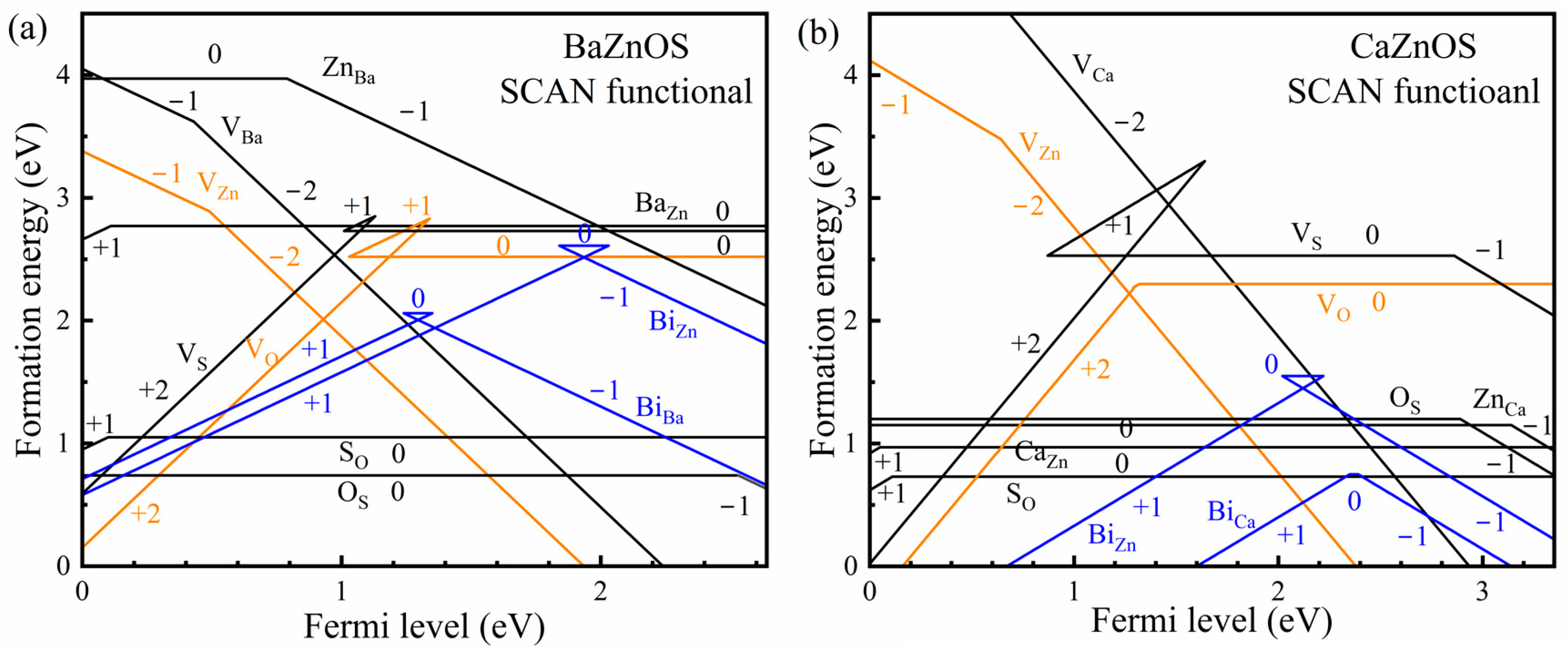
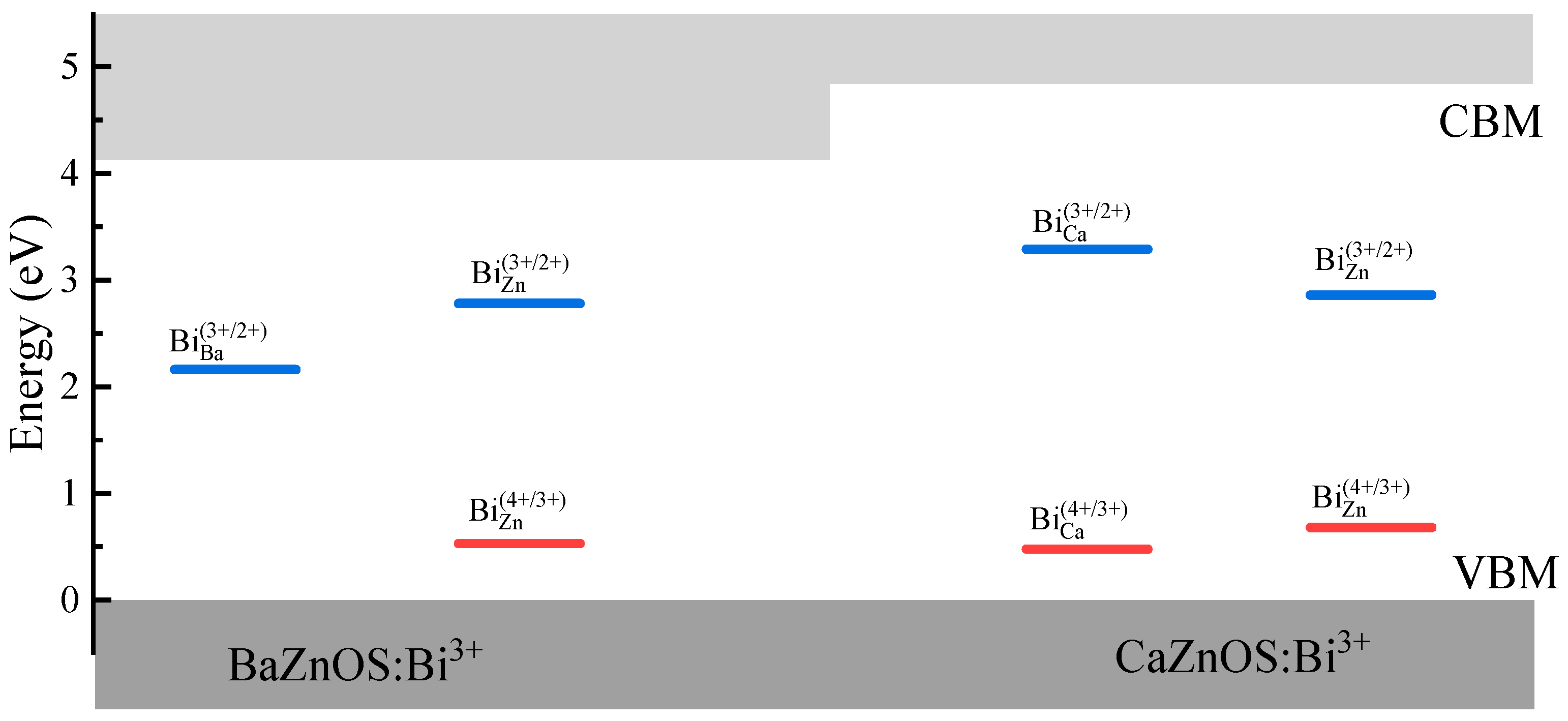
3.2. Formation of the Intrinsic Defects and Bi Dopants

Figure 3 shows the formation energies of the intrinsic defects, including A site or Zn cation vacancies (VCa, VBa or VZn), oxygen vacancies (VO), sulfur vacancies (VS), cation antisite defects (CaZn, ZnCa, BaZn and ZnBa), anion antisite defects (OS, SO), as well as those of Bi substituting the A sites or Zn sites (BiCa, BiBa or BiZn). In Figure 3, the employed chemical potentials of the components are determined by considering the following conditions. In the formation of AZnOS compounds from raw materials (AS and ZnO bulks), there is an enthalpy change Δ H = μ A Z n O S ( b u l k ) μ A S b u l k μ Z n O b u l k . Since the equation μ A Z n O S ( b u l k ) = μ A + μ Z n + μ O + μ S is linked with the stable A Z n O S compounds, the Δ H can be equally separated in approximation, giving the two following equations:
μ A + μ S = μ A S b u l k + Δ H / 2
μ Z n + μ O = μ Z n O b u l k + Δ H / 2 .
Avoiding confusion from the choice of reference, the following equations are introduced: μ A = μ A b u l k + Δ μ A , μ Z n = μ Z n b u l k + Δ μ Z n , μ O = 1 / 2 μ O 2 g a s + Δ μ O , μ S = μ S b u l k + Δ μ S , which can be used to rewrite Equations (1) and (2). Meanwhile, we take the condition of Δ μ A = Δ μ S and Δ μ Z n = Δ μ O for reference, and ignore the overall shift of chemical potential Δ H / 4 for all the elements, where the values of Δ H are calculated to be 0.03 eV and 0.87 eV for A = Ca and Ba, respectively. The referenced element chemical potentials are as follows:
Δ μ A = Δ μ S = 1 / 2 ( μ A S b u l k μ A b u l k μ S b u l k )
Δ μ Z n = Δ μ O = 1 / 2 ( μ Z n O b u l k μ Z n b u l k 1 / 2 μ O 2 g a s ) .
The defect concentration is related to the Gibbs energy of formation. For solid phases, it is always approximated by the formation energy, expressed as follows: c / N s i t e s = ω e x p ( E f / k B T ) , where the defect concentration c is strongly influenced by the parameter E f (formation energy) rather than by T (the temperature at which the defects reach thermal equilibrium distribution), N s i t e s (the numbers of available atomic sites), or ω (the degeneracy factor of defects). For the two AZnOS (A = Ba, Ca) hosts, the Fermi levels are dominated by the charge balance between the cation and anion vacancies located close to the valance band, as shown by the orange line of V Z n 2 and V O 2 + in Figure 3. The formation energies of the antisite defects (OS and SO) show lower formation energies at around 1.0 eV in the two AZnOS, acting as the dominant intrinsic defects. However, the formation of OS and SO defects hardly influences the Fermi level of materials, as they are always in neutral charge states. The antisite defects between the two cation sites show quite different properties for the two AZnOS. The formation energies of the CaZn and ZnCa antisite defects in CaZnOS are about 1.0 eV, remarkably lower than the BaZn and ZnBa defects in BaZnOS. This is consistent with the large ionic radii differences between the Ba2+ ions and Zn2+ ions. The VO and VS defects are mainly in “+2” charge states for the two AZnOS, and the formation energies of VO are slightly lower than those of VS. The VCa, VBa, and VZn defects are in “ 2 ” charge states, where the VZn defects show the lowest formation energy.
With the doping of bismuth ions, e.g., increasing the amount of Bi2O3 during preparation, the Fermi level will increase and the charge balance case will shift from V Z n 2 and V O 2 + to V Z n 2 and B i C a + in CaZnOS:Bi3+ materials. The doped bismuth ions are mainly “+3” charge states in CaZnOS:Bi3+, and it is easier for Bi3+ ions to substitute the Ca2+ site than the Zn2+ site. The concentration of V Z n 2 defects will remarkably increase, for charge balance, the B i C a + defects. In BaZnOS:Bi3+ materials, the doped bismuth ions are also in “+3” charge states, no matter whether Bi ions substitute the Ba2+ or Zn2+ sites. The formation energies of B i B a + and B i Z n + defects are similar, and the Bi3+ dopants slightly prefer occupying the Zn2+ cation sites. Meanwhile, the formation energies of B i B a + and B i Z n + defects are close to the V O 2 + defects in BaZnOS:Bi3+; the Fermi level position and the intrinsic defect concentration in BaZnOS:Bi3+ are hardly influenced by the Bi3+ doping amount adjustment. In short, the site occupancies and the charge states of the dopants can be determined well by the formation energy calculations, which are greatly consistent with those from the empirical model [10]. And the charge state of the Bi ions in the Ba site of BaZnOS is also in the trivalent rather than the divalent state.

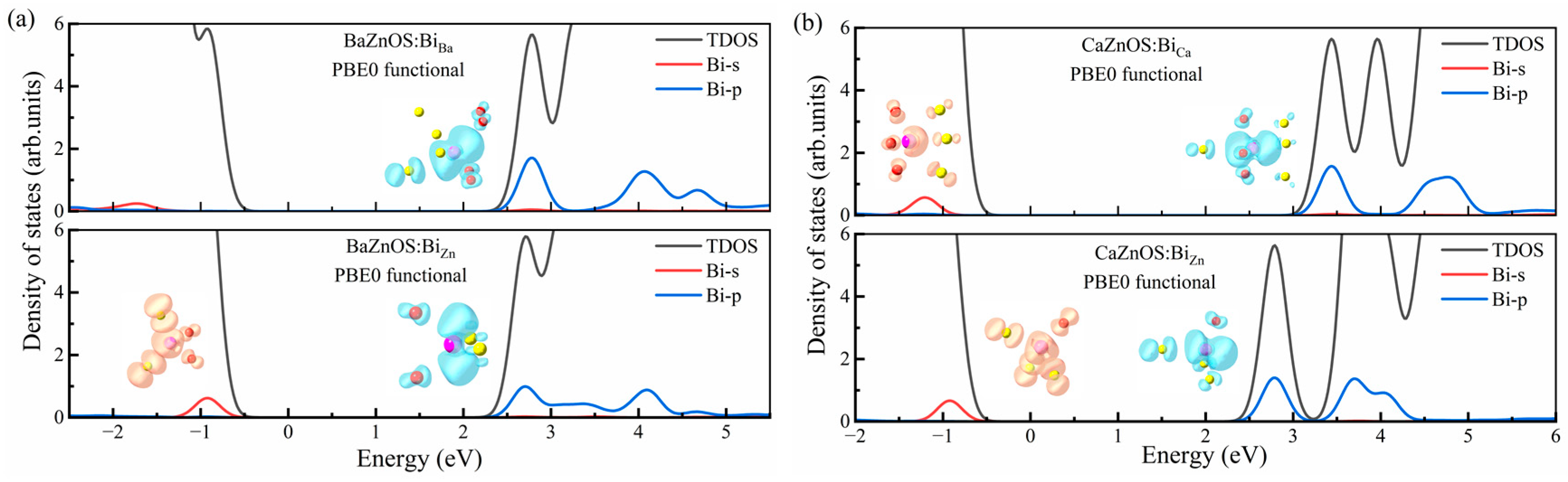
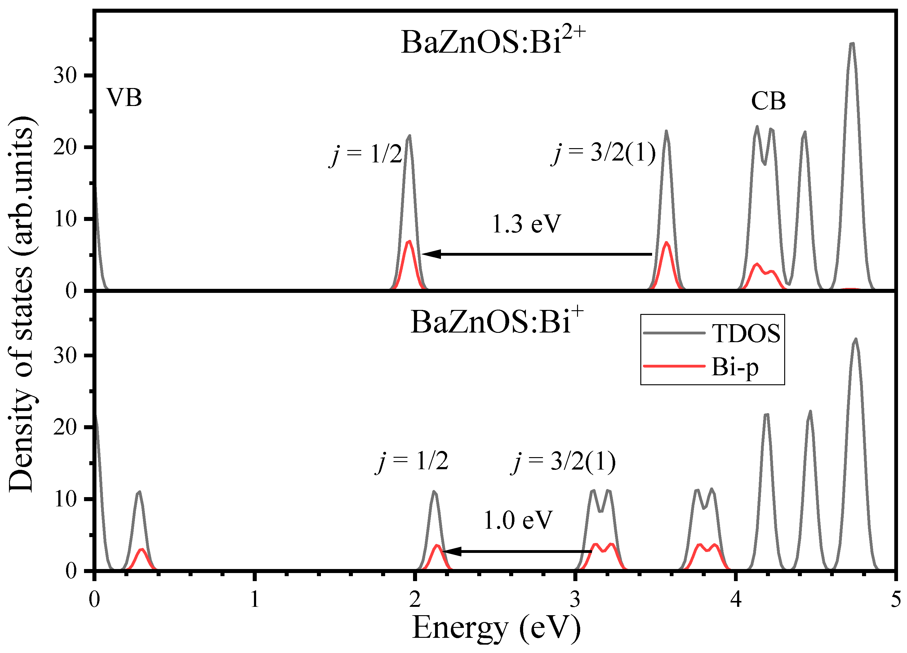
3.3. Electronic Properties of Bi3+ Dopants

Figure 4 shows the partial DOSs of 6s and 6p orbitals in Bi3+ in the ground states of AZnOS:Bi3+ (A = Ca, Ba), which were calculated with the PBE0 functional that included SOC. In the two hosts, the 6p orbitals of Bi3+ dopants are always near the CBM, no matter whether Bi3+ substitutes A sites or Zn sites. The 6s orbitals of Bi3+ dopants are near the VBM in the Zn sites, while the 6s orbitals are deep in the valence band for Bi3+ when substituting the A sites. The Bi3+-6s orbital together with the ligand O-2p and S-3p orbital form an anti-bonding orbital, whose energy position is determined by the nephelauxetic effect between the Bi3+ ion and the ligands. The Bi3+-6s orbital contains substantial contributions from the p orbitals of the nearest three oxygen ligands and three sulfur ligands. Thus, the S-3p orbitals, which dominate the top of the valence band, contribute more to the localized Bi3+-6s state than the O-2p orbitals. In Figure 4, the charge density profiles of the hole and electron localized on the Bi3+-6s and Bi3+-6p orbitals, respectively, are also plotted in order to exhibit such picture more intuitive. Compared to the dispersed Bi3+-6s orbitals, the Bi3+-6p orbital was mainly distributed along the one axis. For the Bi3+ dopants substituting the Ca sites in CaZnOS:Bi3+, the next-nearest sulfur with a bond length of ~3.5 Å has also contributed to the Bi3+-6s orbitals. This clearly shows that the geometric structure relaxation properties of Bi dopants in different charge states are correlated with the electronic structure of the Bi 6s and 6p orbitals.
In our previous work [24], it was pointed out that the luminescence processes of Bi3+ dopants can be predicted by their defect levels in the band gaps, e.g., (1) the 3P0,1 emission will dominate when the Bi3+ ions act as both stable electron and electron traps; (2) the CT emission will dominate when the Bi3+ ions act as stable electron traps only; (3) the MMCT emission will dominate when the Bi3+ ions act as stable hole traps only. As shown in Figure 5, thermodynamic charge transition levels calculated by the PBE0 functional are used to describe the trap depths of Bi3+ ions acting as hole or electron traps. In BaZnOS:Bi3+, the ( 4 + / 3 + ) transition levels of Bi ions in the A sites cannot be found in the band gap, and the doped Bi3+ ions only act as deep electron traps. Thus, the CT (Bi2+ + hVBM) excited state is predicted to be the lowest excited state and dominates the emission for Bi3+ ions in the A sites, which is calculated to be 1.54 eV. For Bi3+ substituting the Zn sites of BaZnOS:Bi3+, the ( 4 + / 3 + ) and ( 3 + / 2 + ) transition levels are both in the band gap. Thus, the lowest Bi3+ excited state should be 3P0,1, which can give an emission energy of 1.74 eV. For CaZnOS:Bi3+, regardless of whether Bi3+ substitutes the A sites or the Zn sites, ( 4 + / 3 + ) and ( 3 + / 2 + ) transition levels are always in the band gap, and the 3P0,1 excited states will always dominate the emission. The 3P0,1 emission energies of Bi3+ dopants are calculated to be 2.57 eV in A sites and 1.56 eV in Zn sites.
Considering the above site occupancy studies, we confirm that the experimentally measured strong broad emission band, peaking at about 485 nm (2.55 eV) in CaZnOS:Bi3+, originates from the 3P0,1 excited state of Bi3+ in the Ca site. The dominant broad emission band, peaking at about 627nm (1.97 eV) in BaZnOS:Bi3+, originated from the 3P0,1 excited state of Bi3+ in the Zn site. Although we improved the assignments of the dominant emission in AZnOS:Bi3+ (A = Ca, Ba), the additional emission peaking at about 507 nm (2.44 eV) in BaZnOS remains unknown and requires further studies of the detailed luminescence mechanism.

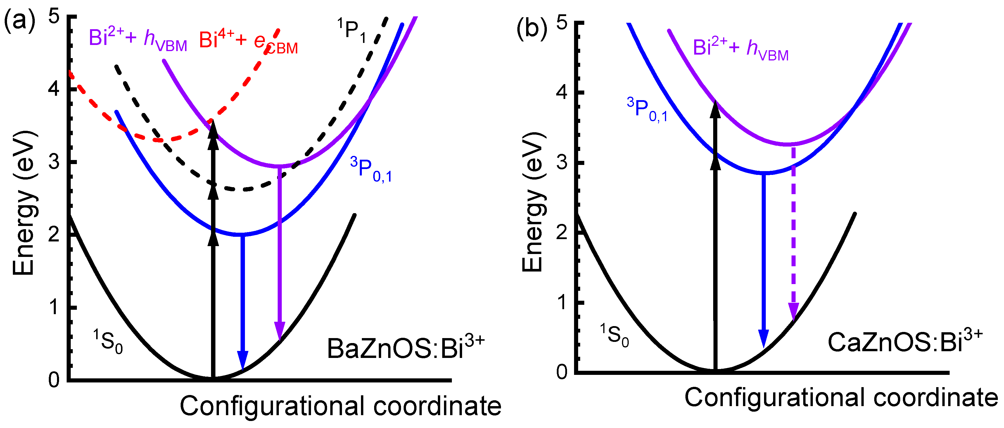
3.4. Excitation and Luminescence of Bi3+ Dopants

Based on the optimized equilibrium structures for both ground and various Bi3+-related excited states for the two hosts, we obtain the excitation and emission energies for various transitions, as listed in Table 1. To illustrate the luminescence processes, a schematic configuration coordinate diagram is constructed based on these results, as shown in Figure 6. For Bi3+ substituting the Zn site in BaZnOS, the A band, CT, and MMCT excitation energies are 2.29, 3.60, and 3.67 eV, respectively, according to our calculations. Using the 6s6p excited state splitting in PBE0 + SOC calculations [27], we estimated the 1S0   1P1 excitation to be 2.91 eV. Since the 3P0,1 is the lowest excited state, all the above excitations together with the host related absorption, approximated by the band gap 4.13 eV, were able to provide 3P0,1 emission. This is consistent with the various excitation bands in the experiment peaking at about 450 nm (2.75 eV), 366 nm (3.38 eV), and 297 nm (4.17 eV). However, the CT emission is the metastable excited state, and it requires special excitation energy to induce the corresponding emission, as shown in Figure 6. In the experiment, the broad excitation band peaking at around 366 nm (3.39 eV) provides a strong CT emission at around 507 nm (2.25 eV), which shows great agreement with our calculations. For the 3P0,1 emission of Bi3+ ions in CaZnOS, the dominant excitation and emission are both the 1S0   3P0,1 transition for Bi3+ substituting the Ca sites, as shown in Figure 6. Furthermore, our calculation shows that the emission energy of the CT excited state for Bi3+ in the Ca sites of CaZnOS:Bi3+ is similar to the 3P0,1 emission. The calculated energies of 1S0 3P0,1 excitation (3.23 eV) and CT emission (2.57 eV) are consistent with the measured optical transition bands peaking at 366 nm (3.39 eV) and 485 nm (2.56 eV). In the experiment, the CT excitation of Bi3+ in Ca sites was not obviously found in the excitation spectra, which may be covered by the stronger host-related excitation at around 275 nm (4.50 eV). It is noted that the dual-emission caused by the metastable excited state has also been observed in CaSnO3:Bi3+, while lower temperature is required to observe the emission with shorter wavelength [24].
Furthermore, since the lower valence-state Bi ions, such as Bi2+ and Bi+, were considered to be the reason for the extra red emission of BaZnOS:Bi, we studied their optical transition energies. The emissions of Bi2+ and Bi+ dopants in BaZnOS were estimated to be 1.6 eV and 1.0 eV, respectively, by the Kohn–Sham orbitals according to the methods of Ref. [27], as shown in Figure 7. Although the calculated 2P3/2(1)  2P1/2 emission of Bi2+ was consistent with the measured emission band peaking at 627 nm, this does not support that emission origin from Bi2+ ions. First, the Bi2+ ions are not expected to be the dominant charge state in these two materials, as shown in the formation energy diagrams above. It requires a precise adjustment of the environment to meet the Fermi level for the formation of stable Bi2+ ions. Second, the measured excitation spectra show strong agreement with the Bi3+ ions, rather than that of the Bi2+ dopants in BaZnOS estimated by the Kohn–Sham orbitals. Third, the measured fluorescence decay curves [10] show the average decay time of emissions of 485 nm in CaZnOS:Bi (773 ns), 507 nm in BaZnOS:Bi (1.34 ns), and 627 nm in BaZnOS:Bi (884 ns). If the 627 nm emission is assigned to Bi2+ ions, the 485 nm emission in CaZnOS:Bi can also be assigned to Bi2+ ions considering the similar decay time. In short, with the combination of formation energy and optical transition energy calculations, we successfully reveal the site-selective occupancy and the luminescence processes, which helps to improve the reassignment of excitation and emission spectra and understand the dual-emission in the BaZnOS:Bi3+ system.

4. Conclusions

In our work, the first-principles calculations were performed to study the mono- and dual-emission properties of Bi3+ dopants in the oxysulfide AZnOS (A = Ca, Ba). The local environments of the dopants and the formation energies of the defects in AZnOS:Bi3+ systems were studied. The results show that the Bi3+ ions mainly occupy the Zn sites of BaZnOS hosts and the Ca sites of CaZnOS hosts. By calculating the defect levels and the electronic structures, the optical luminescence properties of Bi3+ dopants were obtained in the two hosts, which were in great agreement with the measurements. The excitation and emission bands were reassigned, where the 3P0,1 emissions were dominant in both CaZnOS:Bi3+ and BaZnOS:Bi3+ phosphors, acting as the emission band with lower energies. The additional emission band in BaZnOS:Bi3+ originates from the CT state, a metastable excited state. However, the CT emission energy of CaZnOS:Bi3+ is similar to that of 3P0,1 emission and the excited state is not as stable as BaZnOS:Bi3+. These all result in the difference between mono- and dual-emission in AZnOS:Bi3+ (A = Ca, Ba) systems. Furthermore, the possibility of Bi ions with lower charge states, such as Bi2+ and Bi+, was discussed and excluded. Our results provide the basis for novel material design and emission tuning for Bi3+-doped materials.

Author Contributions

Conceptualization, B.L. and M.G.B.; software, Q.K.; validation, Q.K., B.L., and M.G.B.; formal analysis, Q.K. and B.L.; investigation, Q.K. and B.L; resources, B.L. and M.G.B.; data curation, Q.K. and B.L.; writing—original draft preparation, Q.K. and B.L.; writing—review and editing, B.L. and M.G.B.; supervision, B.L. and M.G.B.; project administration, B.L. and M.G.B.; funding acquisition, B.L. and M.G.B. All authors have read and agreed to the published version of the manuscript.

Funding

B.L. was financially supported by the National Natural Science Foundation of China (Grant No. 12304439), the China Postdoctoral Science Foundation (Grant No. 2023MD744135), the Science and Technology Research Program of Chongqing Municipal Education Commission (Grant No. KJQN202200629), and the Joint Innovative Development Project of Chongqing Municipal Natural Science Foundation (Grant No. CSTB2024NSCQ-LZX0047). M.G.B. appreciates support from the Ministry of Science, Technological Development, and Innovation of the Republic of Serbia (451-03-47/2023-01/200017), the China–Serbia Intergovernmental Science and Technology Cooperation Program (Grant No. 2024[7]/6-10), the Specialized Funding Program for the Gathering of 100 Elite Talents in Chongqing, and the Overseas Talents Plan (Grant No. 2022[60]); the latter two are both offered by Chongqing Association for Science and Technology.

Institutional Review Board Statement

Not applicable.

Informed Consent Statement

Not applicable.

Data Availability Statement

The original contributions presented in the study are included in the article; further inquiries can be directed to the corresponding authors.

Conflicts of Interest

The authors declare no conflicts of interest.

References

  1. Khan, S.; Choi, H.; Lee, S.Y.; Lee, K.-R.; Ntwaeaborwa, O.M.; Kim, S.; Cho, S.-H. Unexpected Roles of Interstitially Doped Lithium in Blue and Green Light Emitting Y2O3:Bi3+: A Combined Experimental and Computational Study. Inorg. Chem. 2017, 56, 12139–12147. [Google Scholar] [CrossRef]
  2. Liu, P.; Zhang, Y.; Li, B.; Han, L.; Xu, Y. Trap depth engineering in MgGa2O4:Bi3+ for muticolor dynamic anti-counterfeiting; encryption and optical temperature sensing applications. Chem. Eng. J. 2022, 437, 135389. [Google Scholar] [CrossRef]
  3. Peng, S.; Liu, L.; Wang, L.; Rong, R.; Song, L.; You, W.; Shi, J.; Zhang, Y. A novel self-activated ultraviolet persistent luminescence material and its anti-counterfeiting application based on intensity and time resolution from persistent luminescence. J. Rare Earths 2022, 40, 1417–1423. [Google Scholar] [CrossRef]
  4. Chen, Y.; Chen, J.; Tong, Y.; Zhang, W.; Peng, X.; Guo, H.; Huang, D. Y4GeO8:Er3+,Yb3+ up-conversion phosphors for optical temperature sensor based on FIR technique. J. Rare Earths 2021, 39, 1512–1519. [Google Scholar] [CrossRef]
  5. Xu, Y.; Li, G.; Guan, X.; Wei, Y.; Zhang, M. Synthesis, crystal structure and photoluminescence properties of novel double perovskite La2CaSnO6:Eu3+ red-emitting phosphors. J. Rare Earths 2022, 40, 1682–1690. [Google Scholar] [CrossRef]
  6. Gao, Z.H.; Fu, F.Y.; Niu, L.L.; Jin, M.; Wang, X.H. Emission-tunable Ba2Y1−xScxNbO6:Bi3+ (0 ≤ x ≤ 1.0) phosphors for white LEDs. J. Rare Earths 2022, 40, 1819–1826. [Google Scholar] [CrossRef]
  7. Jin, M.; Zheng, W.; Gong, Z.; Huang, P.; Li, R.; Xu, J.; Cheng, X.; Zhang, W.; Chen, X. Unraveling the triplet excited-state dynamics of Bi3+ in vacancy ordered double perovskite Cs2SnCl6 nanocrystals. Nano Res. 2022, 15, 6422–6429. [Google Scholar] [CrossRef]
  8. Lou, B.; Wen, J.; Ning, L.X.; Yin, M.; Ma, C.-G.; Duan, C.-K. Understanding the defect levels and photoluminescence in a series of bismuth-doped perovskite oxides: First-principles study. Phys. Rev. B 2021, 104, 115101. [Google Scholar] [CrossRef]
  9. Lyu, T.; Dorenbos, P.; Li, C.; Li, S.; Xu, J.; Wei, Z. Unraveling electron liberation from Bi2+ for designing Bi3+-based afterglow phosphor for anti-counterfeiting and flexible X-ray imaging. Chem. Eng. J. 2022, 435, 135038. [Google Scholar] [CrossRef]
  10. Pan, D.; Yang, Y.; Yang, X.; Xu, T.; Cui, Y.; Sun, X.; Feng, H.; Liu, L.; Shen, Y.; Zhao, J.; et al. The effect of site occupation and valence state of Bi on the luminescence properties of Bi-activated oxysulfide MZnOS (M = Ca, Ba) with layer structure. J. Alloys Compd. 2018, 742, 1037–1045. [Google Scholar] [CrossRef]
  11. Li, X.; Zheng, Y.; Ma, R.; Huang, Z.; Wang, C.; Zhu, M.; Jiang, F.; Du, Y.; Chen, X.; Huang, B.; et al. Broadband multimodal emission in Sb-doped CaZnOS-layered semiconductors. Sci. China Mater. 2021, 65, 1329. [Google Scholar] [CrossRef]
  12. Yang, Y.; Li, Q.; Yang, X.; Yang, W.; An, R.; Li, T.; Zhou, Y.; Zhang, H.; Zhao, J.; Zhang, Z. Color manipulation of Bi3+-activated CaZnOS under stress with ultra-high efficiency and low threshold for anticounterfeiting applications. J. Mater. Chem. C 2020, 8, 3308–3315. [Google Scholar] [CrossRef]
  13. Yang, Y.; Yang, X.; Yuan, J.; Li, T.; Fan, Y.; Wang, L.; Deng, Z.; Li, Q.; Wan, D.; Zhao, J.; et al. Time-resolved bright red to cyan color tunable mechanoluminescence from CaZnOS:Bi3+,Mn2+ for anti-counterfeiting device and stress sensor. Adv. Opt. Mater. 2021, 9, 2100668. [Google Scholar] [CrossRef]
  14. Yuan, J.; Yang, Y.; Yang, X.; Fan, Y.; Li, T.; Huang, M.; Zhang, F.; Li, Q.; Zhao, J.; Zhang, Z. Regulating the trap distribution to achieve high-contrast mechanoluminescence with an extended saturation threshold through co-doping Nd3+ into CaZnOS:Bi3+,Li+. J. Mater. Chem. C 2021, 9, 7689–7696. [Google Scholar] [CrossRef]
  15. Liu, M.Z.; Duan, C.K.; Tanner, P.A.; Ma, C.G.; Wei, X.T.; Yin, M. Understanding photoluminescence of Cs2ZrCl6 doped with post-transition-metal ions using first-principles calculations. Phys. Rev. B 2022, 105, 195137. [Google Scholar] [CrossRef]
  16. Zhang, Z.J.; Feng, A.; Zhang, S.L.; Zhang, W.B.; Yang, W. Mechanical properties of layered oxysulfide CaZnOS from first principle calculations. J. Alloys Compd. 2016, 670, 41–47. [Google Scholar] [CrossRef]
  17. Sun, J.; Ruzsinszky, A.; Perdew, J.P. Strongly Constrained and Appropriately Normed Semilocal Density Functional. Phys. Rev. Lett. 2015, 115, 036402. [Google Scholar] [CrossRef]
  18. Kresse, G.; Furthmüller, J. Efficient iterative schemes for Ab initio total-energy calculations using a plane-wave basis set. Phys. Rev. B 1996, 54, 11169–11186. [Google Scholar] [CrossRef]
  19. Blöchl, P.E. Projector augmented-wave method. Phys. Rev. B 1994, 50, 17953–17979. [Google Scholar] [CrossRef]
  20. Paier, J.; Hirschl, R.; Marsman, M.; Kresse, G. The Perdew–Burke–Ernzerhof exchange-correlation functional applied to the G2-1 test set using a plane-wave basis set. J. Chem. Phys. 2005, 122, 234102. [Google Scholar] [CrossRef] [PubMed]
  21. Freysoldt, C.; Grabowski, B.; Hickel, T.; Neugebauer, J.; Kresse, G.; Janotti, A.; Van Dewalle, C.G. First-Principles Calculations for Point Defects in Solids. Rev. Mod. Phys. 2014, 86, 253. [Google Scholar] [CrossRef]
  22. Durrant, T.R.; Murphy, S.T.; Watkins, M.B.; Shluger, A.L. Relation between image charge and potential alignment corrections for charged defects in periodic boundary conditions. J. Chem. Phys. 2018, 149, 024103. [Google Scholar] [CrossRef]
  23. Liu, M.Z.; Duan, C.K.; Hao, R.J.; Yin, M. Luminescence Mechanism of ns2 Ions in Cs2(Sn/Hf)Cl6 Revealed by First-Principles Calculations. J. Phys. Chem. C 2023, 127, 3742–3749. [Google Scholar]
  24. Lou, B.; Wen, J.; Cai, J.; Yeung, Y.-Y.; Yin, M.; Duan, C.-K. First-Principles Study of Bi3+-Related Luminescence and Traps in the Perovskites CaMO3 (M = Zr, Sn, Ti). Phys. Rev. B 2021, 103, 075109. [Google Scholar] [CrossRef]
  25. Perdew, J.P.; Burke, K.; Ernzerhof, M. Generalized gradient approximation made simple. Phys. Rev. Lett. 1996, 77, 3865. [Google Scholar] [CrossRef] [PubMed]
  26. Wang, Y.Z.; Chen, B.; Zhang, X.; Suo, H.; Zheng, W.L.; Shen, J.D.; Li, Y.Y.; Wang, F. Doubly Doped BaZnOS Microcrystals for Multicolor Luminescence Switching. Adv. Opt. Mater. 2022, 10, 2102430. [Google Scholar] [CrossRef]
  27. Chen, Q.; Lou, B.; Jing, W.; Yin, M.; Yeung, Y.-Y.; Su, L.; Duan, C.-K. First Principles Study on Low Valence States Photoluminescence in Bi-doped M2B5O9Cl Crystals. J. Alloys Compd. 2021, 863, 158704. [Google Scholar] [CrossRef]
Figure 1. The crystal structure of the BaZnOS (a) and CaZnOS (b) hosts.
Materials 18 00657 g001
Figure 2. The band structure calculated with SCAN for (a) BaZnOS and (b) CaZnOS hosts, and the PBE0-calculated total and partial density of states (DOSs) for (c) BaZnOS and (d) CaZnOS hosts.
Materials 18 00657 g002
Figure 3. The formation energy diagrams of the intrinsic defects and the dopants of Bi ions substituting the A site or the Zn site in (a) BaZnOS:Bi3+ and (b) CaZnOS:Bi3+ materials.
Materials 18 00657 g003
Figure 4. The PBE0 + SOC-calculated partial DOSs of Bi3+ 6s and 6p orbitals for the ground state of (a) BaZnOS:Bi3+ and (b) CaZnOS:Bi3+ materials, and the charge density profiles of the Bi3+ 6s and 6p orbitals after the localization of a hole and an electron, respectively.
Materials 18 00657 g004
Figure 5. The thermodynamic charge transition level of Bi3+ dopants in AZnOS (A = Ba, Ca) hosts, where the valence band maximum was set as reference.
Materials 18 00657 g005
Figure 6. The configuration coordinate diagrams of the potential surfaces of Bi3+ as a function of the generalized configuration coordinate for (a) BaZnOS:Bi3+ and (b) CaZnOS:Bi3+ materials, where 1S0, 3P0,1, and 1P1 denote the ground, the lowest triplet, and the singlet 6s6p excited states of Bi3+, respectively. Bi4+ + eCBM simulates Bi4+ with one electron at CBM, representing the lowest MMCT excited state, and Bi2+ + hVBM simulates Bi2+ with a loose hole at VBM, representing the lowest CT excited state.
Materials 18 00657 g006
Figure 7. The emission of Bi2+ and Bi+ ions approximated by the splitting of the 6p Kohn–Sham orbitals.
Materials 18 00657 g007
Table 1. The possible excitation and emission energies of Bi dopants in the two AZnOS (A = Ca, Ba) systems obtained with the PBE0+SOC functional.
3P0,1MMCTCT
CaZnOS:BiCaExcitation3.23/3.95
Emission2.58/2.57
CaZnOS:BiZnExcitation2.314.293.54
Emission1.563.572.18
BaZnOS:BiBaExcitation//3.68
Emission//1.54
BaZnOS:BiZnExcitation2.293.673.60
Emission1.742.992.29
Disclaimer/Publisher’s Note: The statements, opinions and data contained in all publications are solely those of the individual author(s) and contributor(s) and not of MDPI and/or the editor(s). MDPI and/or the editor(s) disclaim responsibility for any injury to people or property resulting from any ideas, methods, instructions or products referred to in the content.

