1. Introduction
Copper indium gallium selenide (CIGS) is recognized as one of the most promising solar cell materials, which achieves a record efficiency of 23.64% by implementing a rubidium fluoride post-deposition treatment on silver-doped Cu(In,Ga)Se
2 (ACIGS) absorbers [
1]. CIGS exhibits high power conversion efficiency, a good absorption coefficient, superior long-term stability, and a relatively short energy payback time [
2,
3]. Various methods have been utilized for the fabrication of high-quality CIGS absorbers; however, rear interface recombination hinders further efficiency improvement. Therefore, passivating the rear interface of the CIGS absorber can reduce recombination and improve the photovoltaic (PV) performance of CIGS solar cells.
Molybdenum (Mo) is employed as the back contact for the CIGS solar cells. When the precursor thin films are subject to selenization in a high selenium concentration atmosphere, a large-grained and high-quality CIGS absorber with significantly low selenium vacancies can be obtained. In addition, a thin MoSe
2 interlayer spontaneously forms at the Mo/CIGS interface during high-temperature processing, achieving a favorable quasi-ohmic MoSe
2/CIGS contact and enhancing hole extraction [
4]. However, the Mo back contact exhibits strong parasitic absorption, leading to severe optical losses. It is reported that a cliff-like band alignment forms at the MoSe
2/CIGS interface, introducing a high hole transport barrier (
ΦB = 340 mV) [
5]. Furthermore, when the MoSe
2 layer becomes thicker than a certain threshold (≥100 nm), it increases the series resistance (R
s) of the device, resulting in low PV performance. Additionally, the as-formed thick MoSe
2 layer leads to pronounced lattice expansion, degrading the adhesion at the MoSe
2/CIGS interface [
6]. Therefore, developing effective strategies to reduce the thickness of the MoSe
2 layer presents a viable route to improving the efficiency of CIGS solar cells.
The MoO
x layer has been utilized for selecting photo-generated holes from silicon heterojunction (SHJ) solar cells, thereby improving the efficiency [
7]. An ultra-thin MoO
x layer (~10 nm) with a high work function (~5.9 eV) and a wide bandgap (~2.9 eV) has been introduced to the Mo/CIGS interface for rear interface passivation and band alignment adjustment [
8]. The ultra-thin MoO
x interfacial layer significantly reduces carrier recombination and suppresses the formation of a thick MoSe
2 layer, leading to enhanced open-circuit voltage (
Voc) and fill factor (
FF) [
9,
10,
11]. Adjustment of the oxygen vacancy concentration of the MoO
x layer can optimize electrical conductivity and work function, thereby modulating the interfacial transport barrier and the series resistance of the device [
8,
12]. Meanwhile, a thin MoO
x layer can suppress the formation of MoSe
2 at the Mo/CIGS interface [
5], offering a pathway for interface engineering.
Li et al.’s simulation results demonstrate that a thin MoO
x layer not only suppresses the formation of MoSe
2 at the Mo/CIGS interface but also reduces the back-contact barrier and induces the formation of a “spike-like” band alignment [
5]. As a result, holes can be extracted efficiently by the back contact, while electrons are repelled toward the front interface, thereby reducing recombination at the rear interface of the CIGS absorber layer [
5]. He et al. reported that the deposition of the MoO
x layer on the rear interface of the ultra-thin CIGS devices reduced the back barrier height from 43.8 meV to 16.0 meV [
10]. Meanwhile, Zeng et al. fabricated a MoO
x via oxygen plasma treatment on the Mo back contact, which acts as a rear interface passivation layer for effectively suppressing recombination at the rear interface of CIGS and leading to notable improvements in both open-circuit voltage (
Voc) and fill factor (
FF) [
9]. Given that the work function of MoO
x is thickness-dependent, the thickness of the MoO
x layer influences the band alignment and back-barrier properties at the rear interface of the CIGS absorber. Therefore, optimizing the MoO
x thickness is essential for enhancing the performance of CIGS thin-film solar cells.
A thin MoOx rear interface passivation layer has been shown to improve the performance of the lab-scale CIGS solar cells; however, systematic studies on how the MoOx layer affects the performance of CIGS modules remain limited. In this work, through multiple experimental validations, we systematically investigate the interfacial passivation behavior of MoOx layers with various fabrication parameters (absorber annealing atmospheres, MoOx thickness, and the O2 flow rate during the MoOx deposition). By combining current-voltage (J-V) characterization, external quantum efficiency (EQE) analysis, and interfacial microstructure characterization, we establish a quantitative correlation between the MoOx passivation layer and key photovoltaic parameters (Voc, FF, Rs). The quantitative analysis of non-radiative and radiative recombination is utilized to investigate the mechanism of the PV performance improvement by introducing MoOx passivation for the CIGS solar cells. Furthermore, the figures of merit (FoM) based on the Shockley–Queisser (SQ) model were employed to investigate the dominant factor for the enhanced photovoltaic performance of the MoOx-passivated CIGS devices. Finally, the MoOx interface passivation layer is utilized for large-area CIGS modules (1650 mm × 658 mm).
3. Results and Discussion
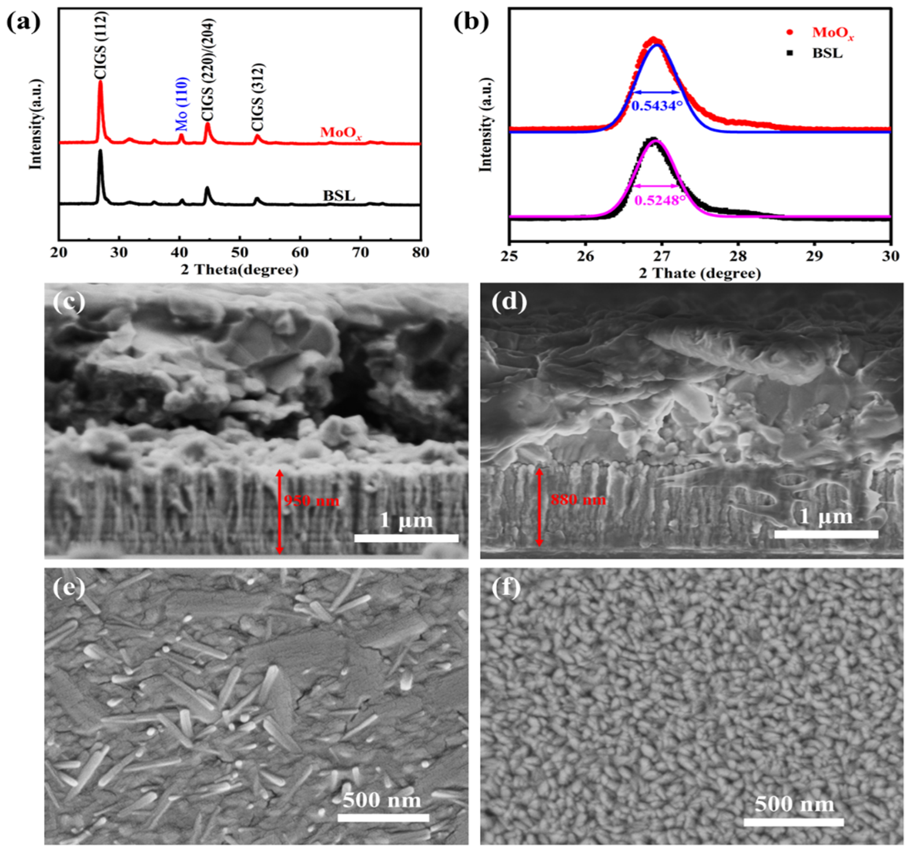
The grazing-incidence X-ray diffraction (GIXRD) patterns of the CIGS samples with/without a MoO
x passivation layer exhibit similar Bragg reflections, as shown in
Figure 1a. The strongest Bragg reflection is located at 27.05°, corresponding to the (112) plane of the CIGS absorber layer [
4]. Additionally, Bragg reflections belonging to the (220)/(204) and (312) planes of the CIGS absorbers are also observed from the GIXRD patterns. Furthermore, the Bragg reflection belonging to the Mo back contact was also observed at 40.4º. In the XRD pattern shown in
Figure 1a, the variation in the peak intensity of Mo (110) (2θ = 40.4°) reflects differences in the relative content of Mo. A higher Mo peak intensity indicates that less Mo has been selenized into MoSe
2, which enhances the adhesion between CIGS and Mo and thereby reduces voids at the CIGS–Mo interface. The full width at half maximum (FWHM) results in
Figure 1b suggest a slight decrease in the crystallinity of CIGS, which is likely attributed to the hindered diffusion of Na after the introduction of the MoO
x layer. The enlarged GIXRD of the patterns in the 25–30° range (
Figure 1b) reveals that the MoO
x-passivated CIGS displayed a broader full width at half maximum (FWHM) of the (112) Bragg reflection than without MoO
x, indicating a reduction in the grain size of the CIGS absorber layer after the introduction of MoO
x. It is reported that gallium (Ga) and oxygen (O) exhibit high chemical reactivity; GaO
x is observed from the interface after sputtering a transparent conductive oxide onto the CIGS surface at room temperature [
13]. Furthermore, when sodium (Na) is present in the precursor film (CuGa:Na layer), it can catalyze the reaction between Ga and O at the high-temperature selenization process, leading to the formation of a thicker GaO
x layer [
14]. Therefore, the reduction in grain size of MoO
x-passivated CIGS absorber can be attributed to the reaction between oxygen species from MoO
x and Ga within the absorber layer.
Figure 1c,d present cross-sectional scanning electron microscopy (SEM) images of the Mo/CIGS back-contact multilayer structure without and with the MoO
x passivation layer, respectively. After the introduction of a MoO
x for rear interface passivation, the back contact thickness is reduced to 880 nm (
Figure 1d) from 950 nm for the case without MoO
x passivation (
Figure 1c). A thinner back contact layer of the MoO
x-passivated CIGS can be explained by the suppression of Se diffusion during the selenization process, which effectively inhibits the formation of a MoSe
2 interfacial layer. Furthermore, the CIGS layer in the MoO
x-passivated sample displays an improved microstructure with significantly fewer voids at the rear interface, indicating that the introduction of MoO
x is beneficial to the elimination of the interfacial issues caused by the thermal expansion coefficient mismatch between the CIGS absorber and the back contact electrode.
Top-view SEM images of the back contact surfaces after removal of the CIGS absorber layer are present in
Figure 1e,f. The needle-like or rod-like Mo(S,Se)
2 nanoparticles are observed from the CIGS without a MoO
x passivation layer (
Figure 1e), indicating that the Mo reacted with Se and S during the high-temperature annealing process. In contrast, when a thin MoO
x layer was deposited on top of the Mo back electrode (
Figure 1f), the morphology of Mo was retained, hindering the formation of Mo(S,Se)
2 nanostructures. This result further confirms that the MoO
x passivation layer can effectively block the diffusion of Se and S toward the Mo back electrode during the high-temperature SAS process.
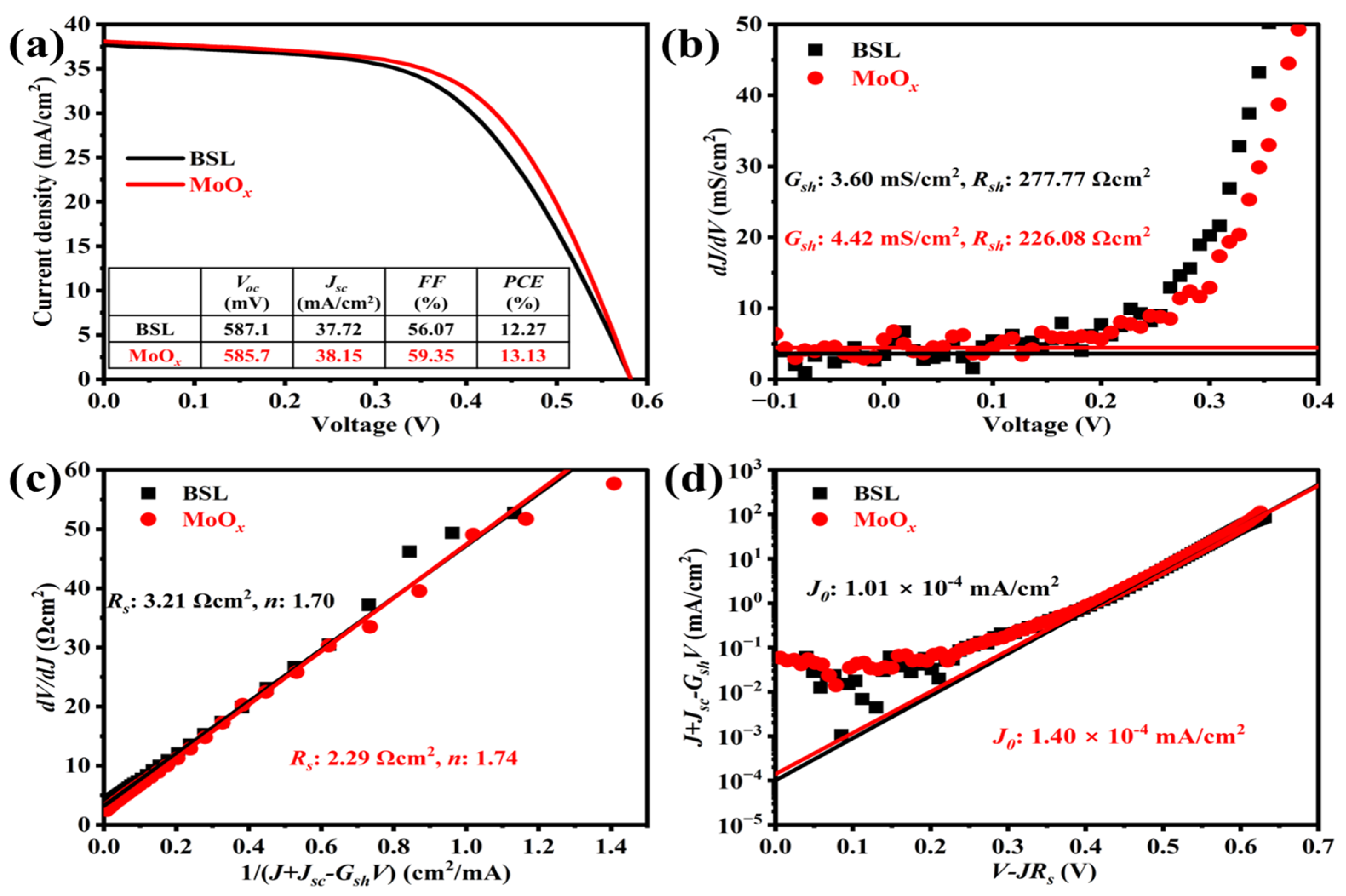
The current density-voltage (
J-V) characteristics of CIGS solar cells with and without the MoO
x rear interface passivation layer are shown in
Figure 2a. The MoO
x-passivated CIGS presents a higher power conversion efficiency (
PCE = 13.13%) than the reference one (
PCE = 12.27%), which can be explained by the increase in both short-circuit current density (
Jsc) and fill factor (
FF). The improvements in
Jsc and
FF can be ascribed to the higher work function of MoO
x than MoSe
2 and Mo [
5], which promotes favorable energy level alignment with the CIGS absorber layer [
5,
10]. This band alignment reduces the hole transport barrier at the rear interface and enhances hole extraction efficiency toward the back electrode [
10]. Moreover, due to the similar device structure and Ga/(Ga+In) (GGI) ratio of the absorber layer in both types of cells—with the only difference being the thin MoO
x modification at the rear interface—their open-circuit voltage (
Voc) values remain comparable.
In terms of electrical parameters, the MoO
x-passivated device exhibits a slightly higher shunt conductance (
Gsh = 4.42 mS/cm
2) than the reference device (
Gsh = 3.60 mS/cm
2) (as shown in
Figure 2b), which may be associated with an increase in the surface roughness of the MoO
x-passivated CIGS (
Figure 1e). Concurrently, after introducing the MoO
x layer, the series resistance decreased from 3.21 Ω·cm
2 to 2.29 Ω·cm
2, while the ideality factor increased slightly from 1.70 to 1.74 (
Figure 2c). These changes indicate more efficient extraction of photogenerated carriers, thereby contributing to the higher
Jsc observed in
Figure 2a. However, likely due to the slightly reduced crystallinity of the CIGS absorber after MoO
x passivation (
Figure 1b), the reverse saturation current density (
J0) also increased to some extent (
Figure 2d).
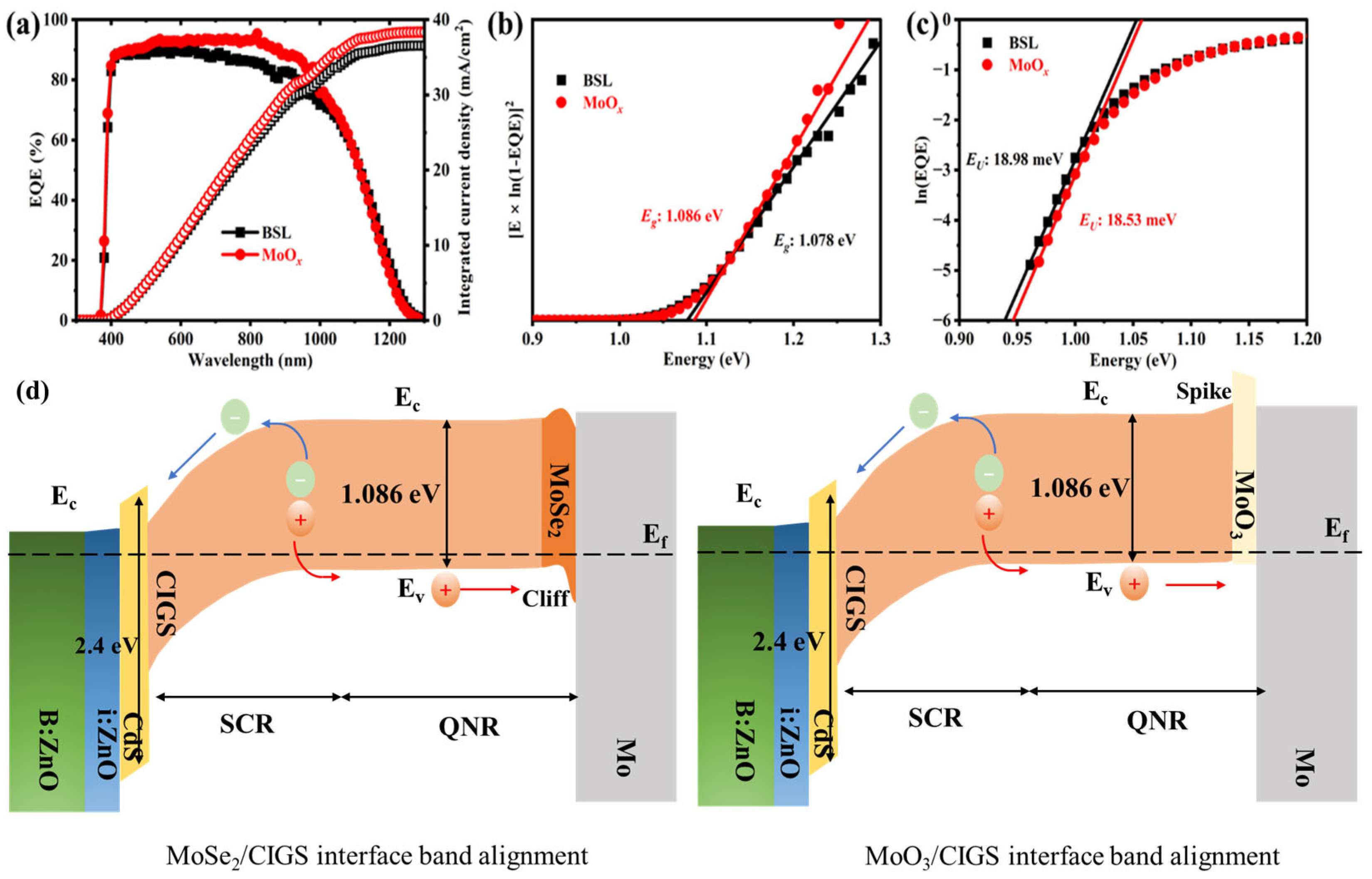
In the wavelength range of 350–420 nm, an overlap in the external quantum efficiency (EQE) spectral response is observed, which is attributed to the optical absorption of the i-ZnO and B:ZnO window layers. Compared to the reference CIGS, the MoO
x-passivated CIGS cell exhibits a higher EQE response across the 450–1050 nm spectral range (
Figure 3a). This enhancement can be correlated with the reduced void density at the rear interface region (as evidenced by the cross-sectional morphology in
Figure 1d). The improved microstructure of the rear interface is favorable to reducing parasitic absorption from the Mo back electrode, thereby enhancing the photocurrent contribution in this spectral region. Owing to the superior EQE response in the visible to near-infrared range, the MoO
x-passivated CIGS achieves a higher integrated current density (
Figure 3a), which is in good agreement with the
J-V measurement results (
Figure 2a).
The bandgap energy of the absorber layer, derived from the EQE spectra, is determined to be 1.086 eV for the MoO
x-passivated CIGS, slightly larger than the 1.078 eV of the reference sample (
Figure 3b). The slightly higher bandgap may be attributed to the fact that the introduction of the MoO
x layer suppresses the reaction between sulfur and the Mo back electrode during the post-sulfurization process. As a result, more sulfur participates in the reaction within the CIGS absorber layer, partially substituting Se in the lattice or passivating selenium vacancies, leading to an increased sulfur content in the absorber and a slight widening of the bandgap. Furthermore, the MoO
x-passivated CIGS exhibits a reduction in the Urbach energy (
Figure 3c), indicating that the rear interface passivation does not degrade the crystalline quality of the CIGS absorber.
The most critical electronic effect of replacing the native MoSe
2 with a MoO
3 interlayer is the modification of the energy band alignment at the back contact. This is schematically illustrated in
Figure 3d, where the reference MoSe
2/CIGS interface, a “cliff-like” valence band offset, is typically formed. This alignment creates a significant energy barrier for hole transport from the CIGS valence band into the back contact, while failing to effectively block electrons, leading to pronounced interface recombination. In contrast, the MoO
3/CIGS interface facilitates a “spike-like” band alignment. The high work function (~5.9 eV) and wide bandgap (~2.9 eV) of MoO
3 cause a strong upward band bending in the CIGS absorber near the interface. This creates a beneficial energy spike in the conduction band, which efficiently blocks electrons from reaching the back contact, redirecting them toward the front junction. Simultaneously, the alignment creates a near-ideal, low-barrier pathway for hole extraction from the CIGS valence band into the MoO
3 layer and subsequently to the Mo electrode. Therefore, the MoO
3 interlayer serves not merely as a passive barrier but as an active interface engineer.
Based on the principles of black-body radiation theory and external quantum efficiency (EQE) data, the radiative voltage (Voc,rad) can be calculated from the radiative saturation current density (J0,rad) and integrated current density from the EQE responses of the solar cell. Combining the Voc,SQ, Voc,rad, and Voc can quantitatively obtain the contributions of radiative recombination losses, non-radiative recombination losses, and total recombination losses. Furthermore, applying the detailed balance theory enables the corresponding physical loss mechanisms analysis of solar cells based on the figures of merit (FoM).
The radiative voltage can be calculated using the following Equation [
15,
16]:
where
J0,rad is the radiative saturation current density and
Jsc is the integrated current density of the device.
Jsc can be calculated by the following Equation [
15,
17]:
where
is the photon flux of the AM1.5G solar spectrum.
J0,rad can be calculated by the following Equation [
15,
16]:
where
is the photon flux of the black-body radiation spectrum:
Here, h is Planck’s constant and c is the speed of light in vacuum. Therefore, ϕBB is a function of temperature; increasing the temperature leads to a higher photon flux from the black-body radiator.
Radiative recombination voltage loss:
Non-radiative recombination voltage loss:
After incorporating the MoO
x passivation layer, the bandgap of the CIGS absorber increased by 8 meV (
Figure 3b and
Table 1), leading to a corresponding rise in its Shockley–Queisser (SQ) theoretical limit open-circuit voltage (
Voc,SQ) from 837.0 mV to 844.5 mV (
Figure 4a and
Table 1). Benefiting from the superior spectral EQE response, the MoO
x-modified device achieved a radiative voltage (
Voc,rad) of 802.8 mV, representing a 4.4 mV enhancement over the reference sample. Consequently, based on the black-body radiation theory and utilizing the measured
Voc from the
J-V characterization (
Figure 2a) alongside the EQE data, the total open-circuit voltage loss can be calculated according to the theoretical calculation equation. These results indicate that the total open-circuit voltage loss of the MoO
x-passivated CIGS increased to 258.8 mV from 249.9 mV for reference CIGS (
Figure 4b and
Table 1). The total
Voc loss consists of radiative recombination loss and non-radiative recombination loss (summarized in
Table 1). The MoO
x-passivated device exhibits a higher radiative recombination loss (41.7 mV) and non-radiative recombination loss (217.1 mV) compared to those of the reference CIGS (38.6 mV and 211.3 mV), respectively. Given that the absorber layer fabrication process remained identical except for the introduction of the MoO
x interlayer, the observed increase in voltage losses can be attributed to the presence of the MoO
x layer.
When the incident photon energy is higher than the bandgap of semiconductor materials, electrons can be excited to the conduction band, leaving the holes in the valence band. Photogenerated electrons recombine with holes and release energy in the form of a radiative photon. The introduction of the MoO
x layer suppressed the reaction between S and the Mo back electrode, which forms a wider bandgap CIGS absorber with a high S concentration, leading to partial substitution of Se or passivation of selenium vacancies (
Figure 3b). The incorporation of S contributes to a reduction in the defect state density within CIGS, reducing lattice disorder and improving crystalline quality (smaller
EU in
Figure 3c). Consequently, the MoO
x-passivated CIGS exhibits a higher radiative recombination voltage, accompanied by a slight increase in radiative recombination voltage loss.
Non-radiative recombination voltage losses typically originate from bulk defects, interface or surface defects, and Auger recombination [
18]. When solar cells are subject to low-injection conditions, the Auger recombination can be negligible [
18]. The MoO
x-passivated CIGS exhibits a slight reduction in crystallinity (wider FWHM in
Figure 1b), diode ideality factor (larger
n value in
Figure 2c), and Urbach energy (larger
EU in
Figure 3c); the non-radiative recombination voltage loss of the MoO
x-passivated CIGS is higher than that of the reference CIGS. This phenomenon may be attributed to the introduction of a thick MoO
x layer (20 nm). It is reported that the work function and electrical conductivity of MoO
x are strongly dependent on its thickness, which affects the hole extraction efficiency at the rear interface [
10]. A thinner MoO
x passivation layer can achieve good conductivity and form a beneficial spike-like band alignment between the CIGS absorber and MoO
x, resulting in superior photovoltaic performance [
10]. Therefore, further optimization of the MoO
x layer thickness should be systematically researched for the improvement of the overall optoelectronic performance.
Given the fundamental differences in the Shockley–Queisser (SQ) limit efficiency and corresponding PV parameters across solar cells with different bandgaps, a direct performance comparison without accounting for the bandgap is not reasonable. Therefore, to objectively evaluate solar cell performance, it is necessary to normalize various parameters against their corresponding bandgap-specific SQ limits [
19]. As shown in
Figure 4c, the figures of merit for these parameters are utilized to analyze the performance losses of solar cells.
The reference CIGS solar cell achieves a power conversion efficiency equivalent to 38% of the SQ theoretical limit for its corresponding bandgap, indicating a 62% loss in efficiency. The efficiency loss originates from the current density loss factor (
Fsc = 11%),
FF loss due to the series and parallel resistance (
= 6%),
FF loss associated with V
oc deficit (
= 22%), the non-radiative open-circuit voltage loss factor (
= 20%), and radiative open-circuit voltage loss factor (
= 3%). In contrast, the MoO
x-passivated CIGS reaches 40% of the SQ limit. This improvement is primarily attributed to a reduction in the FF loss related to the V
oc deficit (
= 19%). It has been reported that the MoO
x layer can passivate the rear interface of CIGS solar cells, thereby improving PV performance [
5,
18]. The mechanism involves the suppression of shunt pathways at the rear interface by the MoO
x layer, leading to an enhanced FF. Furthermore, the MoO
x-passivated CIGS device exhibits consistent
Fsc,
, and
with the reference CIGS device, indicating that the introduction of the MoO
x passivation layer does not impede the charge carrier extraction.
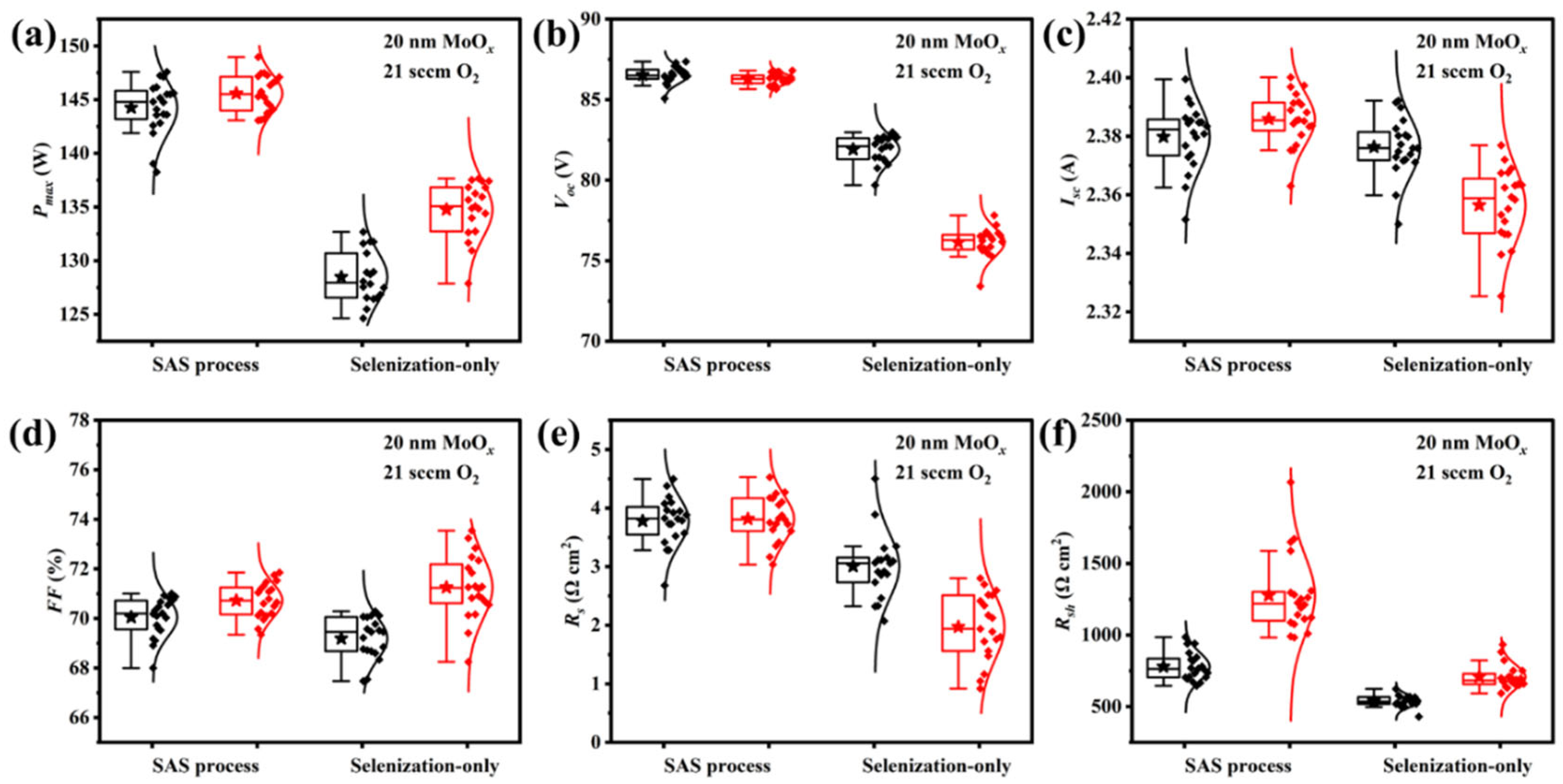
Annealing processes (selenization only or SAS process) would affect the PV performance of CIGS modules without/with a MoO
x passivation layer. The metallic precursor stack without/with a MoO
x passivation layer was subject to selenization only or SAS treatment to evaluate the effect of annealing processes. Regardless of the presence of a MoO
x interface passivation layer, CIGS devices fabricated via the SAS process exhibit a higher maximum output power (
Pmax) compared to those processed with selenization only (
Figure 5). This enhancement is primarily ascribed to the increased
Voc and short-circuit current (
Isc) achieved while maintaining a comparable
FF after SAS treatment (
Figure 5b–d). The SAS-treated CIGS solar cells display an increase in
Rs (
Figure 5e) and
Rsh (
Figure 5f). A larger
Rsh effectively suppresses shunt recombination losses [
18], ultimately leading to superior photovoltaic performance. When the metallic precursor stack without/with a MoO
x passivation layer was subject to selenization only, a higher average
Pmax was observed from the MoO
x-passivated CIGS. Larger Pmax can be attributed to the enhancement in
FF and
Rsh (
Figure 5d,f) as well as the reduction of
Rs (
Figure 5e). It is indicated that no matter whether the absorbers are fabricated from selenization or SAS treatment, the MoO
x layer can passivate the shunt recombination pathway for the improvement in the
Pmax of CIGS solar cells. However, lower
Voc and
Isc are observed from the MoO
x-passivated CIGS solar cells. Therefore, the SAS treatment for the metallic stack is beneficial for better PV performance in the CIGS module.
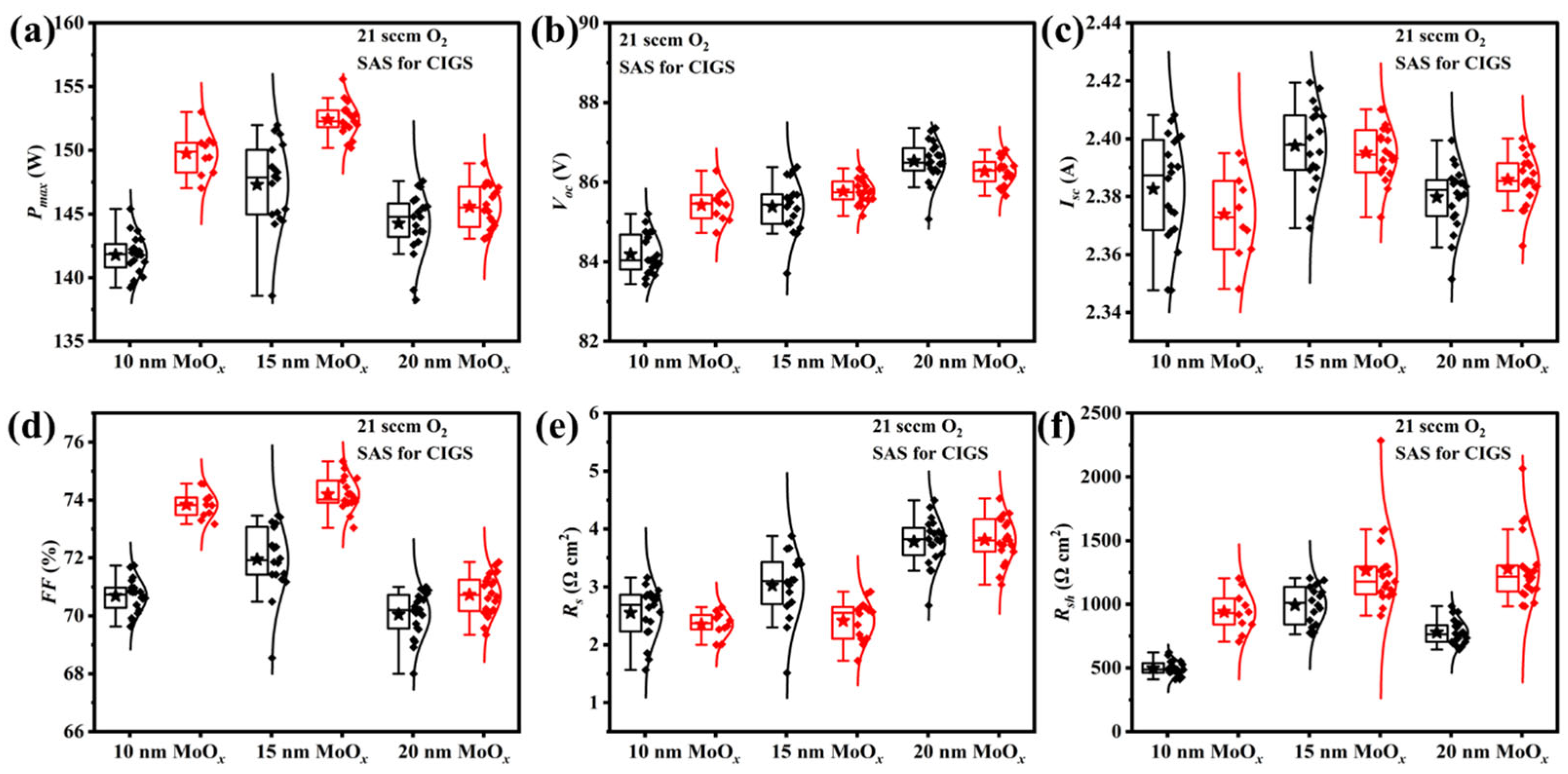
The thickness of the MoO
x layer significantly influences its work function and electrical conductivity [
20]. Therefore, optimizing the MoO
x thickness is crucial for enhancing the rear interface properties and process reproducibility of CIGS solar cells. Experimental results (as shown in
Figure 6) demonstrate that the introduction of a MoO
x rear passivation layer systematically enhances the
Pmax,
Voc, and
FF of CIGS modules.
Isc values initially increase and reach a maximum value at 15 nm, then decrease as the MoO
x thickness is further increased. Nevertheless, the
Isc of the device with a 20 nm MoO
x layer remains higher than that of the device modified with a 10 nm layer. CIGS modules with 10 nm and 20 nm MoO
x passivation layers exhibit
Rs values comparable to the corresponding reference samples. When a 15 nm MoO
x layer was introduced in the rear interface of the CIGS modules, a lower average
Rs was observed. Furthermore, the MoO
x-passivated CIGS modules show higher
Rsh values compared to the corresponding reference samples. These results indicate that the MoO
x layer not only hinders the formation of the MoSe
2 layer and passivates the rear interface but also effectively suppresses interfacial shunt paths, thereby enhancing the device’s
Rsh and comprehensively optimizing the optoelectronic performance.
The oxygen (O
2) flow rate during sputter deposition serves as a critical parameter for modulating the electrical resistivity of MoO
x thin films, thereby directly influencing their carrier transport behavior within the device [
8]. Based on the previously established thickness optimization results, a MoO
x layer thickness of 15 nm was selected for this study to systematically investigate the effect of MoO
x layers—synthesized via reactive sputtering under different O
2 flow rates—on the performance of CIGS solar cells. To mitigate variations carried out in different selenization batches, all MoO
x-passivated samples prepared under various O
2 flow rates, along with their corresponding reference samples, were fabricated using identical sputtering and sulfurization-after-selenization (SAS) process conditions.
No matter whether the MoO
x passivation layer is deposited at various O
2 flow rates, MoO
x-passivated CIGS modules exhibit superior
Pmax compared to the corresponding reference samples (
Figure 7). The enhancement in
Pmax is attributed to the effective suppression of the reaction between Se and the Mo back electrode by the MoO
x layer (larger
FF in
Figure 7d), which promotes the formation of an ohmic contact at the rear interface and consequently optimizes carrier transport [
19]. Additionally, the MoO
x layer increases the
Rsh (
Figure 7f), leading to the suppression of the shunt losses. However, when the MoO
x layer is sputtered at a high O
2 flow rate during sputtering (O
2 flow ≥ 28 sccm), the formation of highly resistive MoO
3 is favored over MoO
x with suitable conductivity [
8]. The high-resistance MoO
3 layer impedes carrier extraction, resulting in the deterioration of device performance.
Based on these systematic research results, the CIGS solar cell fabricated on a 15 nm-thick MoOx layer deposited at an O2 flow rate of 21 sccm, in combination with the sulfurization-after-selenization (SAS) process, demonstrated the optimum performance. The MoOx-passivated device achieved an average output power of 152.41 W (corresponding to a substrate size of 1650 mm × 658 mm), with the key photovoltaic parameters as follows: Voc = 85.77 V, Isc = 2.40 A, FF = 74%, and η = 14.0%.
