
Transparent Electrodes Based on Crack-Templated Metallic Networks for Next-Generation Optoelectronics


Abstract

1. Introduction
2. Conductive Meshes: Material Selection and Properties
2.1. Silver
2.2. Copper
- Haacke’s FoM [88]:
- Coleman’s FoM [89]:
2.3. Gold
2.4. Hybrid and Other Materials
3. Applications in Optoelectronics
3.1. Electroluminescent Devices
3.2. Solar Cells
3.3. Smart Windows
3.4. Other Devices
4. Conclusions and Future Perspectives
Author Contributions
Funding
Institutional Review Board Statement
Informed Consent Statement
Data Availability Statement
Conflicts of Interest
Abbreviations
| CE | Current Efficiency |
| CNTs | Carbon Nanotubes |
| CSMPI | Colorless Shape Memory Polyimide |
| CT | Crack Template |
| ED | Electroless Deposition |
| EIL | Electron Injection Layer |
| EML | Emissive Layer |
| EP | Electroplating |
| EQE | External Quantum Efficiency |
| ETL | Electron Transport Layer |
| FoM | Figure of Merit |
| HIL | Hole Injection Layer |
| HPMC | Hydroxypropyl Methyl Cellulose |
| HTL | Hole Transport Layer |
| ITO | Indium Tin Oxide |
| IZVO | Indium Zinc Vanadium Oxide |
| LCST | Lower Critical Solution Temperature |
| OLED | Organic Light-Emitting Diode |
| OSC | Organic Solar Cell |
| PCE | Power Conversion Efficiency |
| PET | Polyethylene Terephtalate |
| PEN | Polyethylene Naphtalate |
| PDMS | Polydimethylsiloxane |
| PVD | Physical Vapor Deposition |
| PSC | Perovskite Solar Cell |
| Rs | Sheet Resistance |
| TCE | Transparent Conductive Electrode |
| WF | Work Function |
References
- Cao, W.; Li, J.; Chen, H.; Xue, J. Transparent electrodes for organic optoelectronic devices: A review. J. Photonics Energy 2014, 4, 040990. [Google Scholar] [CrossRef]
- Prosa, M.; Benvenuti, E.; Pasini, M.; Giovanella, U.; Bolognesi, M.; Meazza, L.; Galeotti, F.; Muccini, M.; Toffanin, S. Organic Light-Emitting Transistors with Simultaneous Enhancement of Optical Power and External Quantum Efficiency via Conjugated Polar Polymer Interlayers. ACS Appl. Mater. Interfaces 2018, 10, 25580–25588. [Google Scholar] [CrossRef]
- Hofmann, A.; Cloutet, E.; Hadziioannou, G. Materials for Transparent Electrodes: From Metal Oxides to Organic Alternatives. Adv. Electron. Mater. 2018, 4, 1700412. [Google Scholar] [CrossRef]
- Ma, J.; Kim, M.; Jeong, J.; Park, M.; Ha, H.; Kang, S.; Kang, S. Highly Efficient ITO-Free Quantum-Dot Light Emitting Diodes via Solution-Processed PEDOT:PSS Semitransparent Electrode. Materials 2023, 16, 4053. [Google Scholar] [CrossRef]
- López-Naranjo, E.; González-Ortiz, L.; Apátiga, L.; Rivera-Muñoz, E.; Manzano-Ramírez, A. Transparent Electrodes: A Review of the Use of Carbon-Based Nanomaterials. J. Nanomater. 2016, 2016, 1–12. [Google Scholar] [CrossRef]
- Bae, S.; Kim, H.; Lee, Y.; Xu, X.; Park, J.; Zheng, Y.; Balakrishnan, J.; Lei, T.; Kim, H.; Song, Y.; et al. Roll-to-roll production of 30-inch graphene films for transparent electrodes. Nat. Nanotechnol. 2010, 5, 574–578. [Google Scholar] [CrossRef] [PubMed]
- Han, T.; Lee, Y.; Choi, M.; Woo, S.; Bae, S.; Hong, B.; Ahn, J.; Lee, T. Extremely efficient flexible organic light-emitting diodes with modified graphene anode. Nat. Photonics 2012, 6, 105–110. [Google Scholar] [CrossRef]
- Chen, C.; Dou, L.; Zhu, R.; Chung, C.; Song, T.; Zheng, Y.; Hawks, S.; Li, G.; Weiss, P.; Yang, Y. Visibly Transparent Polymer Solar Cells Produced by Solution Processing. ACS Nano 2012, 6, 7185–7190. [Google Scholar] [CrossRef]
- Wang, S.; Dong, Y.; Li, Y.; Ryu, K.; Dong, Z.; Chen, J.; Dai, Z.; Ke, Y.; Yin, J.; Long, Y. A solar/radiative cooling dual-regulation smart window based on shape-morphing kirigami structures. Mater. Horiz. 2023, 10, 4243–4250. [Google Scholar] [CrossRef]
- Kwon, N.; Kim, K.; Sung, S.; Yi, I.; Chung, I. Highly conductive and transparent Ag honeycomb mesh fabricated using a monolayer of polystyrene spheres. Nanotechnology 2013, 24, 235205. [Google Scholar] [CrossRef]
- Kim, A.; Won, Y.; Woo, K.; Kim, C.; Moon, J. Highly Transparent Low Resistance ZnO/Ag Nanowire/ZnO Composite Electrode for Thin Film Solar Cells. ACS Nano 2013, 7, 1081–1091. [Google Scholar] [CrossRef] [PubMed]
- Scardaci, V. Copper Nanowires for Transparent Electrodes: Properties, Challenges and Applications. Appl. Sci. 2021, 11, 8035. [Google Scholar] [CrossRef]
- Gong, S.; Zhao, Y.; Shi, Q.; Wang, Y.; Yap, L.; Cheng, W. Self-assembled Ultrathin Gold Nanowires as Highly Transparent, Conductive and Stretchable Supercapacitor. Electroanalysis 2016, 28, 1298–1304. [Google Scholar] [CrossRef]
- Woo, Y. Transparent Conductive Electrodes Based on Graphene-Related Materials. Micromachines 2019, 10, 13. [Google Scholar] [CrossRef]
- Siwal, S.; Saini, A.; Rarotra, S.; Zhang, Q.; Thakur, V. Recent advancements in transparent carbon nanotube films: Chemistry and imminent challenges. J. Nanostructure Chem. 2021, 11, 93–130. [Google Scholar] [CrossRef]
- Sekkat, A.; Sanchez-Velasquez, C.; Bardet, L.; Weber, M.; Jiménez, C.; Bellet, D.; Muñoz-Rojas, D.; Nguyen, V. Towards enhanced transparent conductive nanocomposites based on metallic nanowire networks coated with metal oxides: A brief review. J. Mater. Chem. A 2024, 12, 25600–25621. [Google Scholar] [CrossRef]
- Kumar, S.; Seo, Y. Flexible Transparent Conductive Electrodes: Unveiling Growth Mechanisms, Material Dimensions, Fabrication Methods, and Design Strategies. Small Methods 2024, 8, e2300908. [Google Scholar] [CrossRef]
- Sorrentino, R.; Worsely, R.; Lagonegro, P.; Martella, C.; Alieva, A.; Scavia, G.; Galeotti, F.; Pasini, M.; Dubertret, B.; Brovelli, S.; et al. Hybrid MoS2/PEDOT:PSS transporting layers for interface engineering of nanoplatelet-based light-emitting diodes. Dalton Trans. 2021, 50, 9208–9214. [Google Scholar] [CrossRef]
- Lagonegro, P.; Martella, C.; Squeo, B.; Carulli, F.; Scavia, G.; Lamperti, A.; Galeotti, F.; Dubertret, B.; Pasini, M.; Brovelli, S.; et al. Prolonged Lifetime in Nanocrystal Light-Emitting Diodes Incorporating MoS2-Based Conjugated Polyelectrolyte Interfacial Layer as an Alternative to PEDOT:PSS. ACS Appl. Electron. Mater. 2020, 2, 1186–1192. [Google Scholar] [CrossRef]
- Boota, M.; Pasini, M.; Galeotti, F.; Porzio, W.; Zhao, M.; Halim, J.; Gogotsi, Y. Interaction of Polar and Nonpolar Polyfluorenes with Layers of Two-Dimensional Titanium Carbide (MXene): Intercalation and Pseudocapacitance. Chem. Mater. 2017, 29, 2731–2738. [Google Scholar] [CrossRef]
- Sibu, G.; Gayathri, P.; Akila, T.; Marnadu, R.; Balasubramani, V. Manifestation on the choice of a suitable combination of MIS for proficient Schottky diodes for optoelectronic applications: A comprehensive review. Nano Energy 2024, 125, 109534. [Google Scholar] [CrossRef]
- Jiang, D.; Liu, Z.; Xiao, Z.; Qian, Z.; Sun, Y.; Zeng, Z.; Wang, R. Flexible electronics based on 2D transition metal dichalcogenides. J. Mater. Chem. A 2021, 10, 89–121. [Google Scholar] [CrossRef]
- Zhang, C.; Nicolosi, V. Graphene and MXene-based transparent conductive electrodes and supercapacitors. Energy Storage Mater. 2019, 16, 102–125. [Google Scholar] [CrossRef]
- Kumar, S.; Taunk, M. 2D MXenes for flexible device applications. Mater. Today Phys. 2024, 46, 101483. [Google Scholar] [CrossRef]
- Prosser, J.; Brugarolas, T.; Lee, S.; Nolte, A.; Lee, D. Avoiding Cracks in Nanoparticle Films. Nano Lett. 2012, 12, 5287–5291. [Google Scholar] [CrossRef]
- Adelung, R.; Aktas, O.; Franc, J.; Biswas, A.; Kunz, R.; Elbahri, M.; Kanzow, J.; Schürmann, U.; Faupel, F. Strain-controlled growth of nanowires within thin-film cracks. Nat. Mater. 2004, 3, 375–379. [Google Scholar] [CrossRef]
- Fan, H.; Werner, P.; Zacharias, M. Semiconductor nanowires: From self-organization to patterned growth. Small 2006, 2, 700–717. [Google Scholar] [CrossRef]
- Cui, M.; Zhang, X.; Rong, Q.; Nian, L.; Shui, L.; Zhou, G.; Li, N. High conductivity and transparency metal network fabricated by acrylic colloidal self -cracking template for flexible thermochromic device. Org. Electron. 2020, 83, 105763. [Google Scholar] [CrossRef]
- Gorokhov, E.; Prinz, V.; Noskov, A.; Gavrilova, T. A novel nanolithographic concept using crack-assisted patterning and self-alignment technology. J. Electrochem. Soc. 1998, 145, 2120–2131. [Google Scholar] [CrossRef]
- Xu, B.; Xu, J.; Xia, X.; Chen, H. Large scale lithography-free nano channel array on polystyrene. Lab A Chip 2010, 10, 2894–2901. [Google Scholar] [CrossRef]
- Huntington, M.; Odom, T. A Portable, Benchtop Photolithography System Based on a Solid-State Light Source. Small 2011, 7, 3144–3147. [Google Scholar] [CrossRef] [PubMed]
- Groves, T. Electron beam lithography. In Nanolithography: The Art of Fabricating Nanoelectronic and Nanophotonic Devices and Systems; Woodhead Publishing: Cambridge, UK, 2014; pp. 80–115. [Google Scholar] [CrossRef]
- Wu, D.; Rajput, N.; Luo, X. Nanoimprint Lithography—The Past, the Present and the Future. Curr. Nanosci. 2016, 12, 712–724. [Google Scholar] [CrossRef]
- Suh, Y.; Hong, S.; Lee, J.; Lee, H.; Jung, S.; Kwon, J.; Moon, H.; Won, P.; Shin, J.; Yeo, J.; et al. Random nanocrack, assisted metal nanowire-bundled network fabrication for a highly flexible and transparent conductor. RSC Adv. 2016, 6, S7434–S7440. [Google Scholar] [CrossRef]
- Gupta, N.; Rao, K.; Srivastava, K.; Gupta, R.; Kumar, A.; Marconnet, A.; Fisher, T.; Kulkarni, G. Cosmetically Adaptable Transparent Strain Sensor for Sensitively Delineating Patterns in Small Movements of Vital Human Organs. ACS Appl. Mater. Interfaces 2018, 10, 44126–44133. [Google Scholar] [CrossRef]
- Gong, S.; Yap, L.; Zhu, B.; Zhai, Q.; Liu, Y.; Lyu, Q.; Wang, K.; Yang, M.; Ling, Y.; Lai, D.; et al. Local Crack-Programmed Gold Nanowire Electronic Skin Tattoos for In-Plane Multisensor Integration. Adv. Mater. 2019, 31, e1903789. [Google Scholar] [CrossRef]
- Dong, G.; Liu, S.; Pan, M.; Zhou, G.; Liu, J.; Kempa, K.; Gao, J. Bioinspired High-Adhesion Metallic Networks as Flexible Transparent Conductors. Adv. Mater. Technol. 2019, 4, 1900056. [Google Scholar] [CrossRef]
- Huang, X.; Zhang, F.; Liu, Y.; Leng, J. Active and Deformable Organic Electronic Devices based on Conductive Shape Memory Polyimide. ACS Appl. Mater. Interfaces 2020, 12, 23236–23243. [Google Scholar] [CrossRef]
- Zarei, M.; Li, M.; Medvedeva, E.; Sharma, S.; Kim, J.; Shao, Z.; Walker, S.; Lemieux, M.; Liu, Q.; Leu, P. Flexible Embedded Metal Meshes by Sputter-Free Crack Lithography for Transparent Electrodes and Electromagnetic Interference Shielding. ACS Appl. Mater. Interfaces 2024, 16, 6382–6393. [Google Scholar] [CrossRef]
- Rao, K.; Gupta, R.; Kulkarni, G. Fabrication of Large Area, High-Performance, Transparent Conducting Electrodes Using a Spontaneously Formed Crackle Network as Template. Adv. Mater. Interfaces 2014, 1, 1400090. [Google Scholar] [CrossRef]
- Yan, J.; Wang, Z.; Bai, W.; Wang, C.; Jiang, Y.; Shi, X.; Chen, Y.; Liu, J.; Gao, J. Kill Two Birds with One Stone: Cracking Lithography Technology for High-Performance Flexible Metallic Network Transparent Conductors and Metallic Micronano Sheets. ACS Appl. Mater. Interfaces 2024, 16, 59637–59647. [Google Scholar] [CrossRef]
- Voronin, A.; Fadeev, Y.; Ivanchenko, F.; Dobrosmyslov, S.; Govorun, I.; Podshivalov, I.; Mikhalev, P.; Makeev, M.; Damaratskiy, I.; Ryzhenko, D.; et al. Waste-free self-organized process manufacturing transparent conductive mesh and microflakes in closed cycle for broadband electromagnetic shielding and heater application. J. Mater. Sci.-Mater. Electron. 2025, 36, 62. [Google Scholar] [CrossRef]
- Cama, E.; Pasini, M.; Giovanella, U.; Galeotti, F. Crack-Templated Patterns in Thin Films: Fabrication Techniques, Characterization, and Emerging Applications. Coatings 2025, 15, 189. [Google Scholar] [CrossRef]
- Tomar, B.; Shahin, A.; Tirumkudulu, M. Cracking in drying films of polymer solutions. Soft Matter 2020, 16, 3476–3484. [Google Scholar] [CrossRef]
- Kim, N.; Cho, H.; Kim, Y.; Hwang, J.; Choi, J.; Yu, H. Formation of palladium nano-gap on self-cracked WO3 for hydrogen gas sensors. Int. J. Hydrog. Energy 2023, 48, 1234–1239. [Google Scholar] [CrossRef]
- Lim, M.; Kim, S.; Park, K.; Kim, Y.; Kim, J.; Ok, G.; Choi, S. Facile synthesis of self-aligned gold nanoparticles by crack templated reduction lithography. RSC Adv. 2017, 7, 13228–13231. [Google Scholar] [CrossRef]
- Yamamura, M. Adsorption-mediated nonlinearity of critical cracking thickness in drying nanoparticle-polymer suspensions. Aiche J. 2021, 67, e17229. [Google Scholar] [CrossRef]
- Kiruthika, S.; Rao, K.; Kumar, A.; Gupta, R.; Kulkarni, G. Metal wire network based transparent conducting electrodes fabricated using interconnected crackled layer as template. Mater. Res. Express 2014, 1, 026301. [Google Scholar] [CrossRef]
- Kappert, E.; Pavlenko, D.; Malzbender, J.; Nijmeijer, A.; Benes, N.; Tsai, P. Formation and prevention of fractures in sol-gel-derived thin films. Soft Matter 2015, 11, 882–888. [Google Scholar] [CrossRef]
- Piroird, K.; Lazarus, V.; Gauthier, G.; Lesaine, A.; Bonamy, D.; Rountree, C. Role of evaporation rate on the particle organization and crack patterns obtained by drying a colloidal layer. EPL 2016, 113, 38002. [Google Scholar] [CrossRef]
- Lama, H.; Basavaraj, M.; Satapathy, D. Desiccation cracks in dispersion of ellipsoids: Effect of aspect ratio and applied fields. Phys. Rev. Mater. 2018, 2, 085602. [Google Scholar] [CrossRef]
- Godard, P.; Guillot, A.; Zighem, F.; Thiaudière, D.; Faurie, D.; Renault, P. Strain ratio and thickness effects on plasticity and crack patterns of Nickel thin films. Scr. Mater. 2022, 213, 114638. [Google Scholar] [CrossRef]
- Ghosh, U.; Chakraborty, M.; Bhandari, A.; Chakraborty, S.; DasGupta, S. Effect of Surface Wettability on Crack Dynamics and Morphology of Colloidal Films. Langmuir 2015, 31, 6001–6010. [Google Scholar] [CrossRef]
- Chae, K.; Nguyen, V.; Lee, S.; Phung, T.; Sim, Y.; Seong, M.; Lee, S.; Ahn, Y.; Lee, S.; Ryu, S.; et al. Mechanical failures of Two-Dimensional materials on polymer substrates. Appl. Surf. Sci. 2022, 605, 154736. [Google Scholar] [CrossRef]
- Ding, Y.; Cui, Y.; Liu, X.; Liu, G.; Shan, F. Welded silver nanowire networks as high-performance transparent conductive electrodes: Welding techniques and device applications. Appl. Mater. Today 2020, 20, 100634. [Google Scholar] [CrossRef]
- Liu, P.; Huang, B.; Peng, L.; Liu, L.; Gao, Q.; Wang, Y. A crack templated copper network film as a transparent conductive film and its application in organic light-emitting diode. Sci. Rep. 2022, 12, 20494. [Google Scholar] [CrossRef]
- Wang, Y.; Yan, J.; Wang, Z.; Yang, Z.; Yang, S.; Zhang, K.; Xu, Z.; Geng, Z.; Jiang, Y.; Tian, G.; et al. Micro-Nano Fractal Metal Grids as Transparent Conductive Electrodes for Highly Efficient and Stable Perovskite Solar Cells. ACS Appl. Mater. Interfaces 2025, 17, 18394–18402. [Google Scholar] [CrossRef]
- Kim, Y.; Tak, Y.; Park, S.; Kim, H.; Kim, H. Structural Engineering of Metal-Mesh Structure Applicable for Transparent Electrodes Fabricated by Self-Formable Cracked Template. Nanomaterials 2017, 7, 214. [Google Scholar] [CrossRef]
- Kiruthika, S.; Kulkarni, G. Energy efficient hydrogel based smart windows with low cost transparent conducting electrodes. Sol. Energy Mater. Sol. Cells 2017, 163, 231–236. [Google Scholar] [CrossRef]
- Voronin, A.; Fadeev, Y.; Govorun, I.; Podshivalov, I.; Simunin, M.; Tambasov, I.; Karpova, D.; Smolyarova, T.; Lukyanenko, A.; Karacharov, A.; et al. Cu-Ag and Ni-Ag meshes based on cracked template as efficient transparent electromagnetic shielding coating with excellent mechanical performance. J. Mater. Sci. 2021, 56, 14741–14762. [Google Scholar] [CrossRef]
- Li, T.; Li, S.; Li, X.; Xu, Z.; Zhao, J.; Shi, Y.; Wang, Y.; Yu, R.; Liu, X.; Xu, Q.; et al. A leaf vein-like hierarchical silver grids transparent electrode towards high-performance flexible electrochromic smart windows. Sci. Bull. 2020, 65, 225–232. [Google Scholar] [CrossRef]
- Mondal, I.; Ganesha, M.; Singh, A.; Kulkarni, G. Affordable Smart Windows with Dual-Functionality: Electrochromic Color Switching and Charge Storage. Adv. Mater. Technol. 2023, 8, 2300651. [Google Scholar] [CrossRef]
- Nirmal, K.; Dongale, T.; Khot, A.; Yao, C.; Kim, N.; Kim, T. Ultra-Transparent and Multifunctional IZVO Mesh Electrodes for Next-Generation Flexible Optoelectronics. Nano-Micro Lett. 2025, 17, 12. [Google Scholar] [CrossRef]
- Gupta, R.; Rao, K.; Srivastava, K.; Kumar, A.; Kiruthika, S.; Kulkarni, G. Spray Coating of Crack Templates for the Fabrication of Transparent Conductors and Heaters on Flat and Curved Surfaces. ACS Appl. Mater. Interfaces 2014, 6, 13688–13696. [Google Scholar] [CrossRef] [PubMed]
- Han, B.; Pei, K.; Huang, Y.; Zhang, X.; Rong, Q.; Lin, Q.; Guo, Y.; Sun, T.; Guo, C.; Carnahan, D.; et al. Uniform Self-Forming Metallic Network as a High-Performance Transparent Conductive Electrode. Adv. Mater. 2014, 26, 873–877. [Google Scholar] [CrossRef]
- Rao, K.; Hunger, C.; Gupta, R.; Kulkarni, G.; Thelakkat, M. A cracked polymer templated metal network as a transparent conducting electrode for ITO-free organic solar cells. Phys. Chem. Chem. Phys. 2014, 16, 15107–15110. [Google Scholar] [CrossRef] [PubMed]
- Yang, C.; Merlo, J.; Kong, J.; Xian, Z.; Han, B.; Zhou, G.; Gao, J.; Burns, M.; Kempa, K.; Naughton, M. All-Solution-Processed, Scalable, Self-Cracking Ag Network Transparent Conductor. Phys. Status Solidi A-Appl. Mater. Sci. 2018, 215, 1700504. [Google Scholar] [CrossRef]
- Voronin, A.; Fadeev, Y.; Dobrosmyslov, S.; Simunin, M.; Khartov, S. Random Ag mesh transparent heater obtained with a cracked template technique. J. Phys. Conf. Ser. 2020, 1679, 042087. [Google Scholar] [CrossRef]
- Xu, J.; Qiu, Z.; Yang, M.; Chen, J.; Luo, Q.; Wu, Z.; Liu, G.; Wu, J.; Qin, Z.; Yang, B. Stretchable Transparent Electrode via Wettability Self-Assembly in Mechanically Induced Self-Cracking. ACS Appl. Mater. Interfaces 2021, 13, 52880–52891. [Google Scholar] [CrossRef]
- Kang, S.; Arepalli, V.; Yang, E.; Lee, S.; Wi, J.; Yun, J.; Song, S.; Kim, K.; Eo, Y.; Cho, J.; et al. High Performance and Flexible Electrodeposited Silver Mesh Transparent Conducting Electrodes Based on a Self-Cracking Template. Electron. Mater. Lett. 2022, 18, 440–446. [Google Scholar] [CrossRef]
- Melnychenko, A.; Kudrawiec, R. Crack-Templated Wire-Like Semitransparent Electrodes with Unique Irregular Patterns. ACS Omega 2022, 7, 39181–39186. [Google Scholar] [CrossRef]
- Voronin, A.; Fadeev, Y.; Ivanchenko, F.; Dobrosmyslov, S.; Makeev, M.; Mikhalev, P.; Osipkov, A.; Damaratsky, I.; Ryzhenko, D.; Yurkov, G.; et al. Original concept of cracked template with controlled peeling of the cells perimeter for high performance transparent EMI shielding films. Surf. Interfaces 2023, 38, 102793. [Google Scholar] [CrossRef]
- Kiruthika, S.; Gupta, R.; Rao, K.; Chakraborty, S.; Padmavathy, N.; Kulkarni, G. Large area solution processed transparent conducting electrode based on highly interconnected Cu wire network. J. Mater. Chem. C 2014, 2, 2089–2094. [Google Scholar] [CrossRef]
- Kumar, A.; Pujar, R.; Gupta, N.; Tarafdar, S.; Kulkarni, G. Stress modulation in desiccating crack networks for producing effective templates for patterning metal network based transparent conductors. Appl. Phys. Lett. 2017, 111, 013502. [Google Scholar] [CrossRef]
- Singh, A.; Kiruthika, S.; Mondal, I.; Kulkarni, G. Fabrication of solar and electrically adjustable large area smart windows for indoor light and heat modulation. J. Mater. Chem. C 2017, 5, 5917–5922. [Google Scholar] [CrossRef]
- Pujar, R.; Kumar, A.; Rao, K.; Sadhukhan, S.; Dutta, T.; Tarafdar, S.; Kulkarni, G. Narrowing Desiccating Crack Patterns by an Azeotropic Solvent for the Fabrication of Nanomesh Electrodes. Langmuir 2019, 35, 16130–16135. [Google Scholar] [CrossRef]
- Chen, Z.; Yang, S.; Huang, J.; Gu, Y.; Huang, W.; Liu, S.; Lin, Z.; Zeng, Z.; Hu, Y.; Chen, Z.; et al. Flexible, Transparent and Conductive Metal Mesh Films with Ultra-High FoM for Stretchable Heating and Electromagnetic Interference Shielding. Nano-Micro Lett. 2024, 16, 92. [Google Scholar] [CrossRef]
- Yang, L.; Guan, Y.; Gao, F.; Wan, R.; Wang, P. Effect of crack template structure morphology on electromagnetic shielding efficiency and visual performance of metal mesh optical window. Results Eng. 2025, 25, 103888. [Google Scholar] [CrossRef]
- Urgunde, A.; Kumar, A.; Shejale, K.; Sharma, R.; Gupta, R. Metal Wire Networks Functionalized with Nickel Alkanethiolate for Transparent and Enzymeless Glucose Sensors. ACS Appl. Nano Mater. 2018, 1, 5571–5580. [Google Scholar] [CrossRef]
- Yang, L.; Guo, R.; Gao, F.; Guan, Y.; Zhang, M.; Wang, P. Electromagnetic Interference (EMI) Shielding Performance and Photoelectric Characteristics of ZnS Infrared Window. Materials 2025, 18, 1067. [Google Scholar] [CrossRef]
- Hunger, C.; Rao, K.; Gupta, R.; Singh, C.; Kulkarni, G.; Thelakkat, M. Transparent Metal Network with Low Haze and High Figure of Merit applied to Front and Back Electrodes in Semitransparent ITO-free Polymer Solar Cells. Energy Technol. 2015, 3, 638–645. [Google Scholar] [CrossRef]
- Peng, Q.; Li, S.; Han, B.; Rong, Q.; Lu, X.; Wang, Q.; Zeng, M.; Zhou, G.; Liu, J.; Kempa, K.; et al. Colossal Figure of Merit in Transparent-Conducting Metallic Ribbon Networks. Adv. Mater. Technol. 2016, 1, 6. [Google Scholar] [CrossRef]
- Gedda, M.; Das, D.; Iyer, P.; Kulkarni, G. Work function tunable metal-mesh based transparent electrodes for fabricating indium-free organic light-emitting diodes. Mater. Res. Express 2020, 7, 054005. [Google Scholar] [CrossRef]
- Mondal, I.; Bahuguna, G.; Ganesha, M.; Verma, M.; Gupta, R.; Singh, A.; Kulkarni, G. Scalable Fabrication of Scratch-Proof Transparent Al/F-SnO2 Hybrid Electrodes with Unusual Thermal and Environmental Stability. ACS Appl. Mater. Interfaces 2020, 12, 54203–54211. [Google Scholar] [CrossRef] [PubMed]
- Mondal, I.; Kiruthika, S.; Ganesha, M.; Baral, M.; Kumar, A.; Vimala, S.; Madhuri, P.; Nair, G.; Prasad, S.; Singh, A.; et al. ITO-free large area PDLC smart windows: A cost-effective fabrication using spray coated SnO2 on an invisible Al mesh. J. Mater. Chem. A 2021, 9, 23157–23168. [Google Scholar] [CrossRef]
- Ganesha, M.; Hakkeem, H.; Mondal, I.; Singh, A.; Kulkarni, G. An ITO free All Tungsten-Based Electrochromic Energy Storage Device as Smart Window. Small 2024, 20, e2405467. [Google Scholar] [CrossRef] [PubMed]
- Pham, S.; Ferri, A.; Da Costa, A.; Mohan, M.; Tran, V.; Nguyen, D.; Viville, P.; Lazzaroni, R.; Desfeux, R.; Leclère, P. Nanoscale Electrical Investigation of Transparent Conductive Electrodes Based on Silver Nanowire Network. Adv. Mater. Interfaces 2022, 9, 2200019. [Google Scholar] [CrossRef]
- Haacke, G. New figure of merit for transparent conductors. J. Appl. Phys. 1976, 47, 4086–4089. [Google Scholar] [CrossRef]
- Coleman, J.N.; De, S. Are There Fundamental Limitations on the Sheet Resistance and Transmittance of Thin Graphene Films? ACS Nano 2010, 4, 2713–2720. [Google Scholar]
- Murdoch, G.B. Transparent Conductive Oxides for Organic Electronics; Library and Archives Canada: Ottawa, ON, Canada, 2010. [Google Scholar]
- Liu, H.; Avrutin, V.; Izyumskaya, N.; Ozgur, U.; Morkoç, H. Transparent conducting oxides for electrode applications in light emitting and absorbing devices. Superlattices Microstruct. 2010, 48, 458–484. [Google Scholar] [CrossRef]
- Giovanella, U.; Pasini, M.; Botta, C. Organic Light-Emitting Diodes (OLEDs): Working Principles and Device Technology. In Applied Photochemistry: When Light Meets Molecules; Springer: Cham, Switzerland, 2016; pp. 145–196. [Google Scholar]
- Yan, Y.; Duan, B.; Ru, M.; Gu, Q.; Li, S.; Zhao, W. Toward Flexible and Stretchable Organic Solar Cells: A Comprehensive Review of Transparent Conductive Electrodes, Photoactive Materials, and Device Performance. Adv. Energy Mater. 2024, 15, 2404233. [Google Scholar] [CrossRef]
- Alasmari, A.; Shariq, M.; Alhazmi, N.; Alzahrani, H.; Bouzgarrou, S.; Alkhayri, F.; Alzahrani, A.; Alharbi, S.; Azeez, N. Enhancing perovskite solar cells with graphene-based nanocomposites for sustainable energy: A comprehensive review. Diam. Relat. Mater. 2024, 148, 111517. [Google Scholar] [CrossRef]
- Zhang, J.; Hu, X.; Ji, K.; Zhao, S.; Liu, D.; Li, B.; Hou, P.; Liu, C.; Liu, L.; Stranks, S.; et al. High-performance bifacial perovskite solar cells enabled by single-walled carbon nanotubes. Nat. Commun. 2024, 15, 2245. [Google Scholar] [CrossRef] [PubMed]
- Wan, J.; Chen, Y.; Chen, W.; Xia, J.; Zeng, G.; Cao, J.; Jin, C.; Shen, Y.; Wu, X.; Chen, H.; et al. Enhanced charge collection of AgNWs-based top electrode to realize high-performance, all-solution processed organic solar cells. Sci. China-Chem. 2024, 67, 3347–3356. [Google Scholar] [CrossRef]
- Silva, J.; de Morais, A.; Cesar, R.; Joanni, E.; Teixeira, R.; Marques, F.; de Freitas, J. Investigation of the stability of metallic grids for large-area perovskite solar cells. Sol. Energy Mater. Sol. Cells 2024, 276, 113043. [Google Scholar] [CrossRef]
- Hwang, Y.; Pyun, S.; Choi, M.; Kim, J.; Cho, E. Multi-stimuli-responsive and Multi-functional Smart Windows. Chemnanomat 2022, 8, e202200005. [Google Scholar] [CrossRef]
- Lei, Q.; Wang, L.; Xie, H.; Yu, W. Active-passive dual-control smart window with thermochromic synergistic fluidic glass for building energy efficiency. Build. Environ. 2022, 222, 109407. [Google Scholar] [CrossRef]
- Galeotti, F.; Scatena, L.; Trespidi, F.; Pasini, M. A Comparative Study of Cellulose Ethers as Thermotropic Materials for Self-Tracking Solar Concentrators. Molecules 2022, 27, 8464. [Google Scholar] [CrossRef] [PubMed]
- Xu, G.; Lu, Y.; Zhou, X.; Moloto, N.; Liu, J.; Kure-Chu, S.; Hihara, T.; Zhang, W.; Sun, Z. Thermochromic hydrogel-based energy efficient smart windows: Fabrication, mechanisms, and advancements. Mater. Horiz. 2024, 11, 4867–4884. [Google Scholar] [CrossRef]
- Wu, S.; Sun, H.; Duan, M.; Mao, H.; Wu, Y.; Zhao, H.; Lin, B. Applications of thermochromic and electrochromic smart windows: Materials to buildings. Cell Rep. Phys. Sci. 2023, 4, 101370. [Google Scholar] [CrossRef]
- Gupta, R.; Kumar, A.; Sadasivam, S.; Walia, S.; Kulkarni, G.; Fisher, T.; Marconnet, A. Microscopic Evaluation of Electrical and Thermal Conduction in Random Metal Wire Networks. ACS Appl. Mater. Interfaces 2017, 9, 13703–13712. [Google Scholar] [CrossRef]
- Cheng, C.; Ganguly, S.; Li, P.; Tang, X. Detecting Hypoxia Through the Non-Invasive and Simultaneous Monitoring of Sweat Lactate and Tissue Oxygenation. Biosensors 2024, 14, 584. [Google Scholar] [CrossRef] [PubMed]
- Baëtens, T.; Pallecchi, E.; Thomy, V.; Arscott, S. Cracking effects in squashable and stretchable thin metal films on PDMS for flexible microsystems and electronics. Sci. Rep. 2018, 8, 9492. [Google Scholar] [CrossRef] [PubMed]
- Azani, M.; Hassanpour, A.; Torres, T. Benefits, Problems, and Solutions of Silver Nanowire Transparent Conductive Electrodes in Indium Tin Oxide (ITO)-Free Flexible Solar Cells. Adv. Energy Mater. 2020, 10, 2002536. [Google Scholar] [CrossRef]
- Liu, Z.; Tian, B.; Fan, X.; Zhang, Z.; Liu, J.; Lin, Q.; Shi, P.; Han, F.; Mao, Q.; Jiang, Z. Study on the characteristics of thermo-electrodes of various deposition parameters for the flexible temperature sensor. Rev. Sci. Instrum. 2020, 91, 125004. [Google Scholar] [CrossRef]


| Mesh Material | Metal Deposition Technique | Crack Template Material | Thicknesses | Substrate | Transmittance | Resistance | Figure of Merit (FoM, Coleman) | Applications | Ref. |
|---|---|---|---|---|---|---|---|---|---|
| Ag | Physical vapor deposition | Acrylic resin (CP1), SiO2 (CP2) | 80 nm (Ag) 0.5–30 μm (CP1) 24–150 μm (CP2) | Glass tube; convex lens; round-bottom flask | 86% (CP1) 70% (CP2) | 6 Ω/sq (CP1) 2 Ω/sq (CP2) | 401 (CP1) 482 (CP2) | Transparent heaters, curved surfaces | [64] |
| Ag | Thermal evaporation; Sputtering | TiO2 | ~60 nm (Ag) 1–2 μm (wire width) | PET, glass | >80% (550 nm) | 10 Ω/sq (PET) 4.2 Ω/sq (glass) | 300–900 | Touch screen device | [65] |
| Ag | Vacuum evaporation | Acrylic colloidal suspension | 55 nm (Ag) | Glass | 86% at 550 nm | ~10 Ohm/sq | n.a. | OSC | [66] |
| Ag | Drop casting (AgNWs) | High-stress thin silicon nitride (Si3N4) | 40 nm (AgNW diameter) 1.65–2.05 μm (Si3N4 film) | Silicon wafer | 85% | 0.77 Ω/sq | n.a. | Touch screens | [34] |
| Ag | Electroless deposition; Electroplating | Nail polish/egg white | 100 nm (Ag electroless deposition) 2.5 μm (Ag electroplated) | Glass | 80–82% (pre- and post-electroplating) | 0.008 (pre)–0.01 (post) Ω/sq | Up to 1000 (pre)–208.000 (post) | Transparent conductor for, e.g., OLEDs, thin film solar cells, and EMI shielding | [67] |
| Ag | Electroplating | Egg white/ Nail polish + polyimide (PI) | 100–400 nm (Ag) | Silicon | ~85% | 1.5 Ω/sq | 700–1400 | Photovoltaics | [37] |
| Ag | Sputtering | Acrylic resin | 100 nm (Ag) | PET | ~86% | ~6 Ω/sq | 408 | Thermochromic devices | [28] |
| Ag | Magnetron sputtering | Egg white 1 mL/L (template A) or 3 mL/L (template B) | 200–600 nm (Ag) | PET | 84–91% (550 nm) | 1.6–21 Ω/sq | n.a. | Transparent heaters (e.g., anti-fogging and anti-icing coatings) | [68] |
| Ag(NWs) | Blade coating | Fluoropolymer | 10 μm (wire width) | PDMS | ~90% (550 nm) | 9.8 Ω/sq | 360 | Strain sensors | [69] |
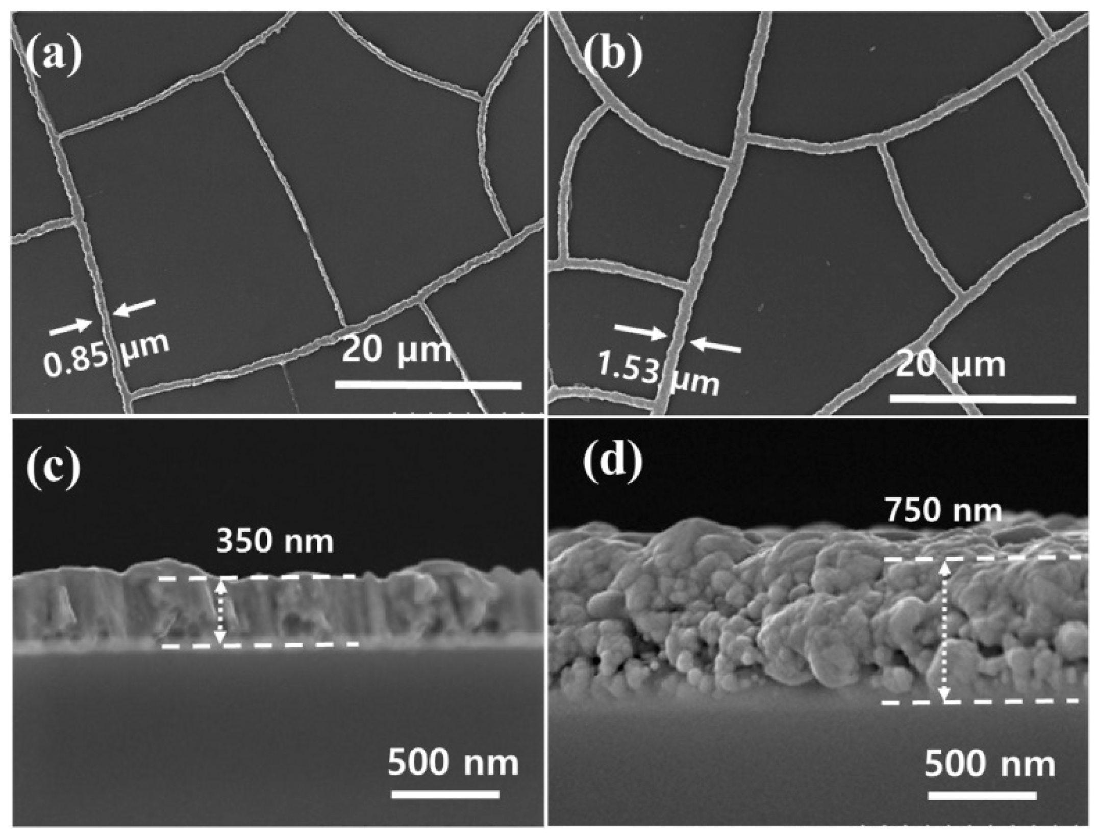
| Ag | Thermal evaporation; Electroplating | Acrylic resin | -Thermally evaporated Ag (TE Ag): 350 nm -EP Ag (EP TE Ag): 750 nm | Glass; PET | TE: 92% EP TE: 88% | 5.7 Ω/sq 1.01 Ω/sq | 2827 | Flexible transparent electrodes | [70] |
| Ag | Thermal evaporation | ZnO + PVP | 200 nm (Ag) 6 μm (crack layer) | Quartz; sapphire; glass | ~83% (550 nm) (quartz > sapphire and glass) | Quartz = 13.55 Ω/sq; sapphire = 10.45 Ω/sq; glass = 13.65 Ω/sq | n.a. | Encryption, solar cells, touch panels, light-emitting diodes, transparent heaters | [71] |
| Ag | Magnetron sputtering | Egg white | 2.5 μm (Ag) 4 nm (PMMA spacer in sandwich structure) | PET | ~89% | 0.28–1.59 Ω/sq | 1303–5495 | EMI shielding | [72] |
| Ag | Magnetron sputtering | Egg white | ~130 μm (cracks) 3–6–10 μm (Ag network, after 1 and 2 wet/dry cycles) 15 μm (Ag-Re micro-nanosheets) | PET | ~88.1% | ~9 Ω/sq | n.a. | Flexible display technologies, lighting, sensing | [41] |
| Ag | Ag ink coating and curing | Acrylic emulsion (CA-600) | ~1.8 μm (Ag) <5 μm widths, 5 μm depths (cracks) | PET | 91–93% | 0.54–1.4 Ω/sq | 4070–7500 | Transparent electrodes and EMI shielding | [39] |
| Ag | Magnetron sputtering | Egg white | 50 μm (egg white) 100–300–600 nm (Ag) 6 μm (wire width) | PET | >80% (500 nm) | ~1.84 Ω/sq | n.a. | Electronic and optoelectronic, EMI shielding | [42] |
| Cu | Electroless deposition; Electroplating | SiO2 (CP1), Acrylic emulsion (CP2) + Pd/Au | 300 nm (EP Cu) 100 nm (ELD Cu) 50–100 μm (CP1 width) 4–8 μm (CP2 width) | PET | 67–75% | 3.8 Ω/sq (ELD + Pd) 0.3 Ω/sq (EP + Au) 1.3 Ω/sq (ELD + Au) | n.a. | Large-area applications (e.g., large panel displays), touch screens and solar cells | [73] |
| Cu | Physical vapor deposition | Acrylic resin | ~1.7 μm (film) ~700 nm (crack width) | Si; PET | 88.2% | 31 Ω/sq | 71–95 | Touch screens, solar cells | [74] |
| Cu | Physical vapor deposition | Acrylic emulsion | 200 nm | PET | ~74% (550 nm) | ~5 Ω/sq | n.a. | Smart windows | [75] |
| Cu | n.a. | Acrylic resin | 80 nm (Cu) ~400 nm (crack width) ~15 μm (crack spacing) | Glass | ~87.5% | 10 Ω/sq | n.a. | Optoelectronic applications (e.g., solar cells, touch screens, transparent heaters) | [76] |
| Cu | Vacuum evaporation | Acrylic suspension | 120 nm | PET | 93% (550 nm) | 13.4 Ω/sq | 380 | OLED | [56] |
| Cu | E-beam evaporation; Electroplating | Acrylic emulsion | 1.7–3.5 μm (Cu) | Ni sheet | 85.8% (550 nm) | 0.18 Ω/sq | 13.232 | EMI shielding | [77] |
| Cu | E-beam evaporation | Acrylic resin + water (DP1) + water and ethylene glycol (DP2) + water and glycerol (DP3) + water and NMP (DP4) | 300 nm (Cu) Crack width: 2–4 μm | Quartz | 80–85% (550 nm) | 6–11 Ω/sq | n.a. | EMI shielding | [78] |
| Au | Vacuum evaporation | TiO2 | ~100 nm (Au) ~10 μm (TiO2) | Glass; quartz; PET | ~82% | 3–6 Ω/sq | n.a. | Optoelectronics | [48] |
| Au | Physical vapor deposition | Crackle paint | n.a. | PET/glass | ~60% | ~4 Ω/sq | n.a. | Enzymeless glucose sensors | [79] |
| Au | E-beam evaporation | Acrylic resin | 300 nm | ZnS | 57.1% to 63.2% (2–10 μm) | 9.5–16.7 Ω/sq | n.a. | EMI shielding | [80] |
| Au, Cu, Ag, Pd, Al, Zn | Physical vapor deposition | Acrylic resin | 90–800 nm (metal wire) 1–4 μm (film) | Glass; quartz; PET | 90.5% (240–3000 nm) | 2.6 Ω/sq (Ag) | n.a. | Transparent, flexible heaters | [40] |
| Ag, Au | Thermal evaporation | Acrylic resin nanoparticles | 20–60 nm (Au/Ag) < 5 μm (wire width) | PEDOT:PSS-coated glass | >80% | <5 Ω/sq | 765 | Polymer solar cells | [81] |
| Ag, Cu | Thermal evaporation and sputtering | Egg white | 60–6000 nm (after electroplating) | PET | 60–95% | 0.03–3 Ω/sq | 10.000–30.000 | LED lighting, solar cells | [82] |
| Cu, Au, Ag | Physical vapor deposition | Crackle precursor (CP) | 50 nm (metal) | Glass | >85% | ~7 Ω/sq | n.a. | OLED | [83] |
| Al | Radio frequency (RF) magnetron sputtering | Silica nanoparticles | ~800 nm (silica) 150 nm (Al) | Glass | ~80% (300–800 nm) | ~20 Ω/sq | 40 < FoM < 90 | Optoelectronics, solar cells | [58] |
| Sn | Physical vapor deposition | Acrylic resin | 400 nm | PET | ~80% (550 nm) | 5 Ω/sq | n.a. | Smart windows | [59] |
| Au/Ag | Thermal evaporation | Crackle paint (BMG1–4) | Ag: 90−105 nm Au: 30−35 nm (Tot: 120–140 nm) Crack width: 2.3 um | Glass | 85% (550 nm) | 5.2 Ω/sq | 428 | White polymer light emitting diodes (WPLEDs) | [38] |
| WO3/Ag | Magnetron sputtering | TiO2 | 30 nm (WO3) 3–10 μm (crack width) | PET | 81% | 1.36 Ω/sq | 377–1247 | Smart windows | [61] |
| Al-SnO2 | Thermal evaporation | Crackle precursor | ~400 nm (Al) ~200 nm (SnO2) | Glass | ~83% (550 nm) | 5.5 Ω/sq | n.a. | Optoelectronics and photovoltaics | [84] |
| Al-SnO2, Au-SnO2 | Thermal evaporation | Acrylic resin | <30 μm | Glass | 85% (Al-SnO2) 92% (Al) 84% (Au-SnO2) | 5 Ω/sq (Al-SnO2) 8–10 Ω/sq (Au-SnO2) | n.a. | Smart windows | [85] |
| Cu-Ag, Ni-Ag | Galvanic deposition (Cu, Ni), Magnetron sputtering (Ag) | Egg white | 1.92 μm (Cu) 0.95 μm (Ni) 200 nm (Ag) | PET | 82–88% (Cu-Ag) 78–87% (Ni-Ag) (550 nm) | 0.06–1.52 Ω/sq (Cu-Ag); 0.7–9.3 Ω/sq (Ni-Ag) | 292 (Ni-Ag)–1785 (Cu-Ag) | EMI shielding | [60] |
| Al_SnO2_WO3 | Thermal evaporation (Al); Spray-pyrolysis (SnO2); Reactive ion sputtering (WO3) | Crackle precursor | 300 nm (Al) | Glass | ~81% (550 nm) | ~5 Ω/sq | n.a. | Smart windows | [62] |
| WO3 | Direct current (DC) sputtering | Colloidal precursor | 260 nm | Glass | 17–74% (550 nm) | 3.2–19.3 Ω/sq | n.a. | Smart windows | [86] |
| V-doped IZO (IZVO) | Magnetron sputtering | Egg yolk | 150 nm (mesh) | PEN | 97% | 21.24 Ω/sq | 3.61 (Ω/sq)−1 (Haacke) | OLED and OSC | [63] |
| Au/ Au+PH1000 | Magnetron sputtering | Egg white/water-based crack glue | ~100 nm | Glass; PEN | 84% (550 nm) | 4 Ω/sq | 566 | Perovskite solar cells (PSC) | [57] |
| Sample | Haacke FoM (Before Drying) [(Ω/sq)−1] | Haacke FoM (After Drying) [(Ω/sq)−1] | Coleman FoM (Before Drying) | Coleman FoM (After Drying) |
|---|---|---|---|---|
| Sample 1 | 7.95 × 10⁻⁴ | 9.2 × 10⁻³ | 8 | 94.7 |
| Sample 2 | 9.1 × 10⁻⁴ | 6.3 × 10⁻³ | 9.3 | 71.2 |
| Sample 3 | 1.7 × 10⁻³ | 7.1 × 10⁻³ | 17 | 86.9 |
| OLED Device | Anode (Mesh) | Hole Injection Layer (HIL) | Hole Transport Layer (HTL) | Emitting Layer (EML) | Electron Transport Layer (ETL) | Electron Injection Layer (EIL) | Cathode | Substrate | Performance | Ref. |
|---|---|---|---|---|---|---|---|---|---|---|
| D1 | Cu Au Ag | TPD | / | Alq3 | BPhen | LiF | Al | Glass | LMAX of 4300 cd/m2, CE of 5.38 cd/A, similar performance to ITO | [83] |
| D2 | Cu | PEDOT:PSS | Alq3 | LiF | Al | Glass | Enhanced L, similar performance to ITO-based devices | |||
| D3 | Cu | PEDOT:PSS | NPB | Alq3 | Alq3 | LiF | Al | PET | LMAX of 1587 cd/m2, 500 bending cycles with minimal Rs change | [56] |
| D4 | IZVO | MoO3 | mCP | DMAC-DPS | DPPS | LiF | Al | PEN | EQE of 18.06%, FoM of 3.61 (Ω/sq)−1, high transmittance (97%) | [63] |
| D5 | Au/Ag | MoO3 | PEDOT:PSS | MEH-PPV:PFO | / | Cs2CO3 | Al | CSMPI film | Turn-on voltage of 5.2 V, CE of 4.3 cd/A, flexible and 3D-formable substrate | [38] |
| Active Material | Mesh Material | JSC (mA/cm2) | VOC (V) | FF (%) | PCE (%) | Ref. |
|---|---|---|---|---|---|---|
| P3HT:PCBM | Ag | ~8.3 (Ag); ~8.6 (ITO) | ~0.60 | ~43–44 | 2.14 (Ag); 2.27 (ITO) | [66] |
| P3HT:PCBM | Ag, Au | ~7.2 (Ag/Ag); ~9.4 (ITO/Ag) | ~0.59–0.62 | ~55–60 | 1.80 (Ag/Ag); 2.25 (ITO/Ag); 3.10 (ITO/Ag opaque) | [81] |
| PM6:Y6:PC71BM | m-IZVO | 27.7 (ITO); >27.7 (m-IZVO) | ~0.689 | ~69 | 14.38 (m-IZVO); 13.17 (ITO) | [63] |
| PTAA:PVK:PCBM:BCP | Au-PH1000 | 21.82 (Au-PH1000); 22.02 (ITO) | 1.11 | 78.99 | 19.17 (Au-PH1000); 20.02 (ITO) | [57] |
Disclaimer/Publisher’s Note: The statements, opinions and data contained in all publications are solely those of the individual author(s) and contributor(s) and not of MDPI and/or the editor(s). MDPI and/or the editor(s) disclaim responsibility for any injury to people or property resulting from any ideas, methods, instructions or products referred to in the content. |
© 2025 by the authors. Licensee MDPI, Basel, Switzerland. This article is an open access article distributed under the terms and conditions of the Creative Commons Attribution (CC BY) license (https://creativecommons.org/licenses/by/4.0/).
Share and Cite
Cama, E.S.; Pasini, M.; Galeotti, F.; Giovanella, U. Transparent Electrodes Based on Crack-Templated Metallic Networks for Next-Generation Optoelectronics. Materials 2025, 18, 3091. https://doi.org/10.3390/ma18133091
Cama ES, Pasini M, Galeotti F, Giovanella U. Transparent Electrodes Based on Crack-Templated Metallic Networks for Next-Generation Optoelectronics. Materials. 2025; 18(13):3091. https://doi.org/10.3390/ma18133091
Chicago/Turabian StyleCama, Eleonora Sofia, Mariacecilia Pasini, Francesco Galeotti, and Umberto Giovanella. 2025. "Transparent Electrodes Based on Crack-Templated Metallic Networks for Next-Generation Optoelectronics" Materials 18, no. 13: 3091. https://doi.org/10.3390/ma18133091
APA StyleCama, E. S., Pasini, M., Galeotti, F., & Giovanella, U. (2025). Transparent Electrodes Based on Crack-Templated Metallic Networks for Next-Generation Optoelectronics. Materials, 18(13), 3091. https://doi.org/10.3390/ma18133091