
Overview on the Thermally Activated Delayed Fluorescence and Mechanochromic Materials: Bridging Efficiency and Versatility in LECs and OLEDs


 and
and 
Abstract
1. Introduction
2. Brief Description of LECs and OLEDs
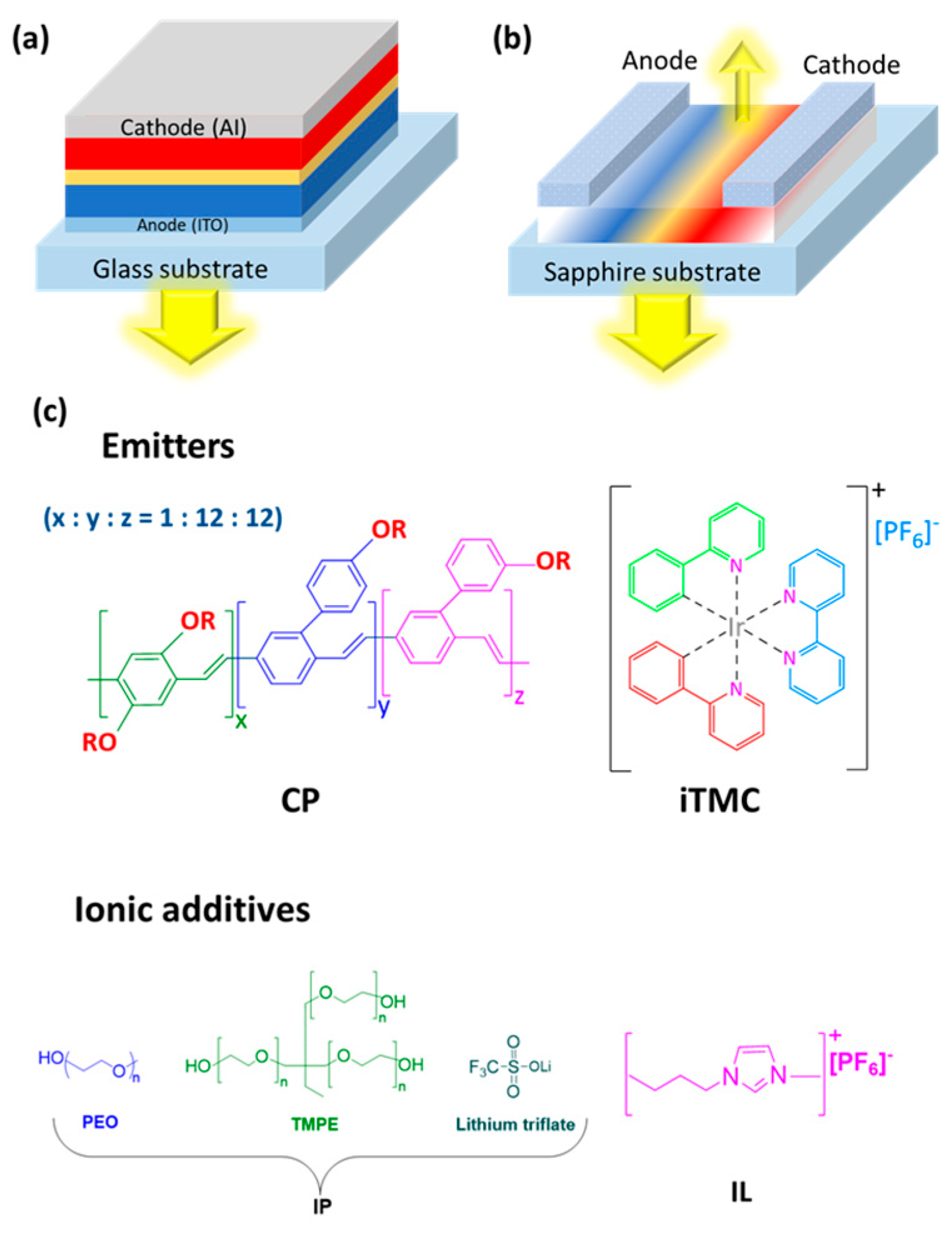
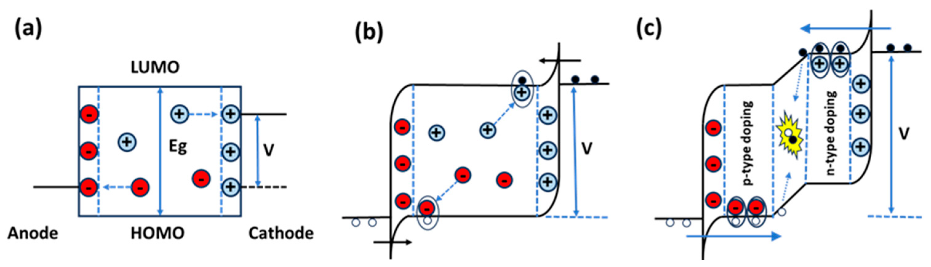
2.1. Differences Between LECs and OLEDs
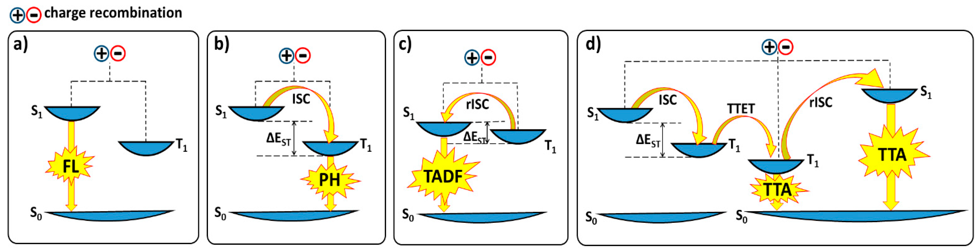
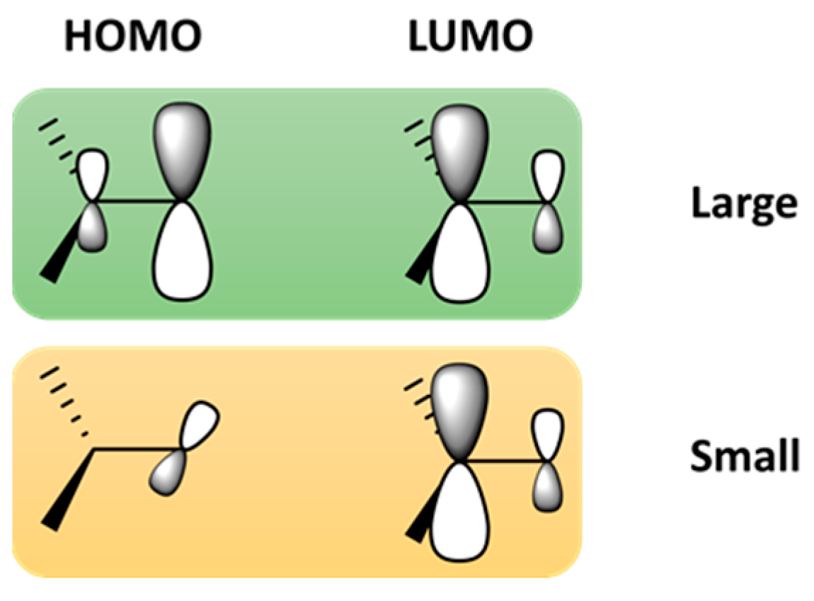
2.2. TADF Mechanism
2.3. Mechanochromic Mechanism
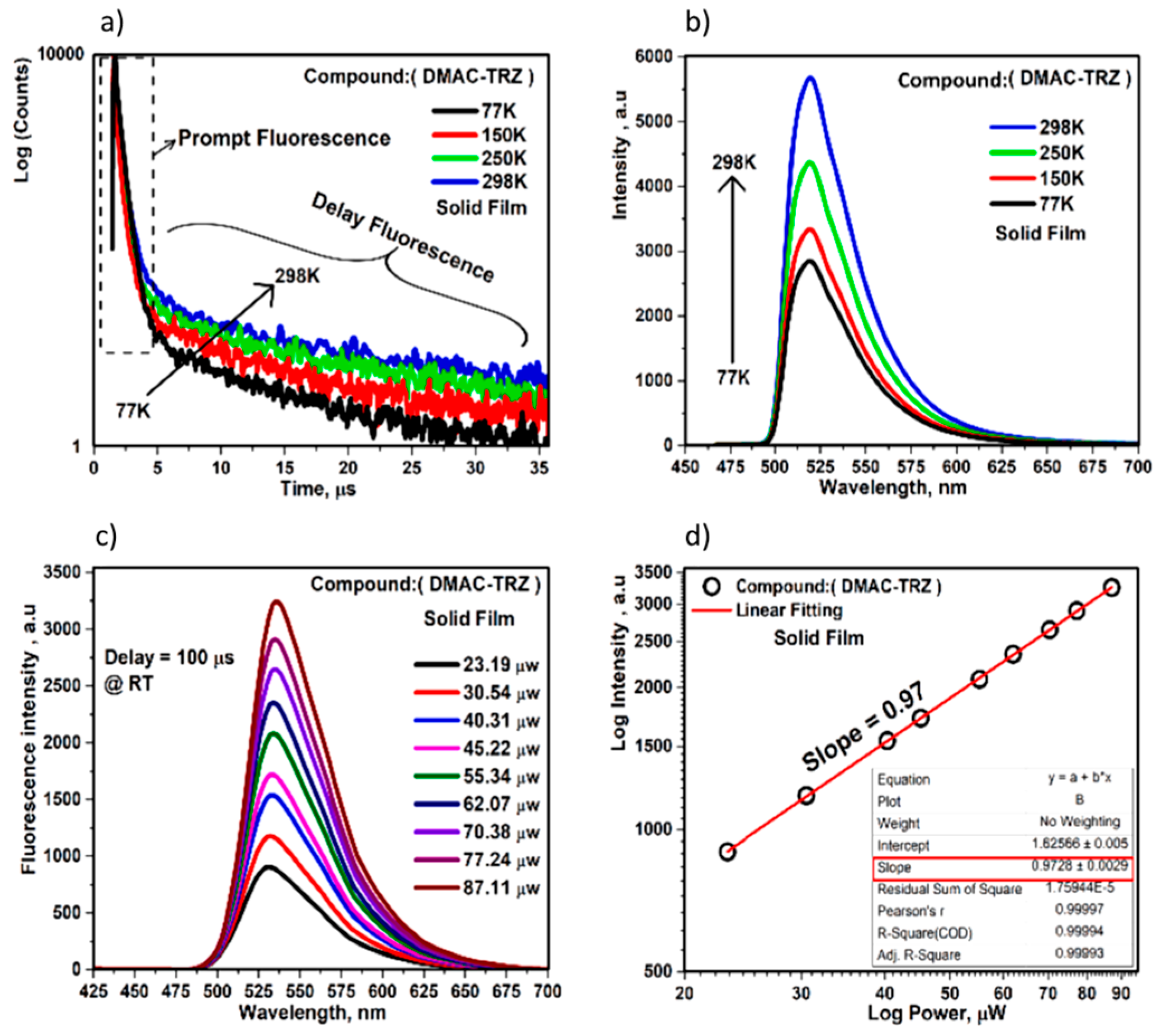
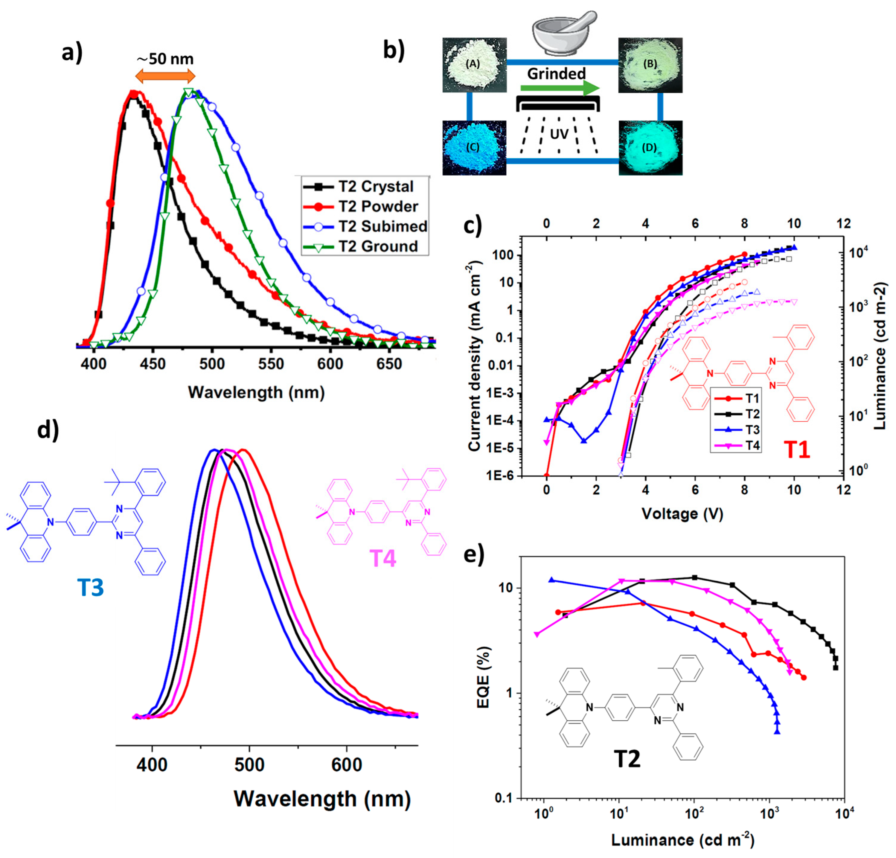
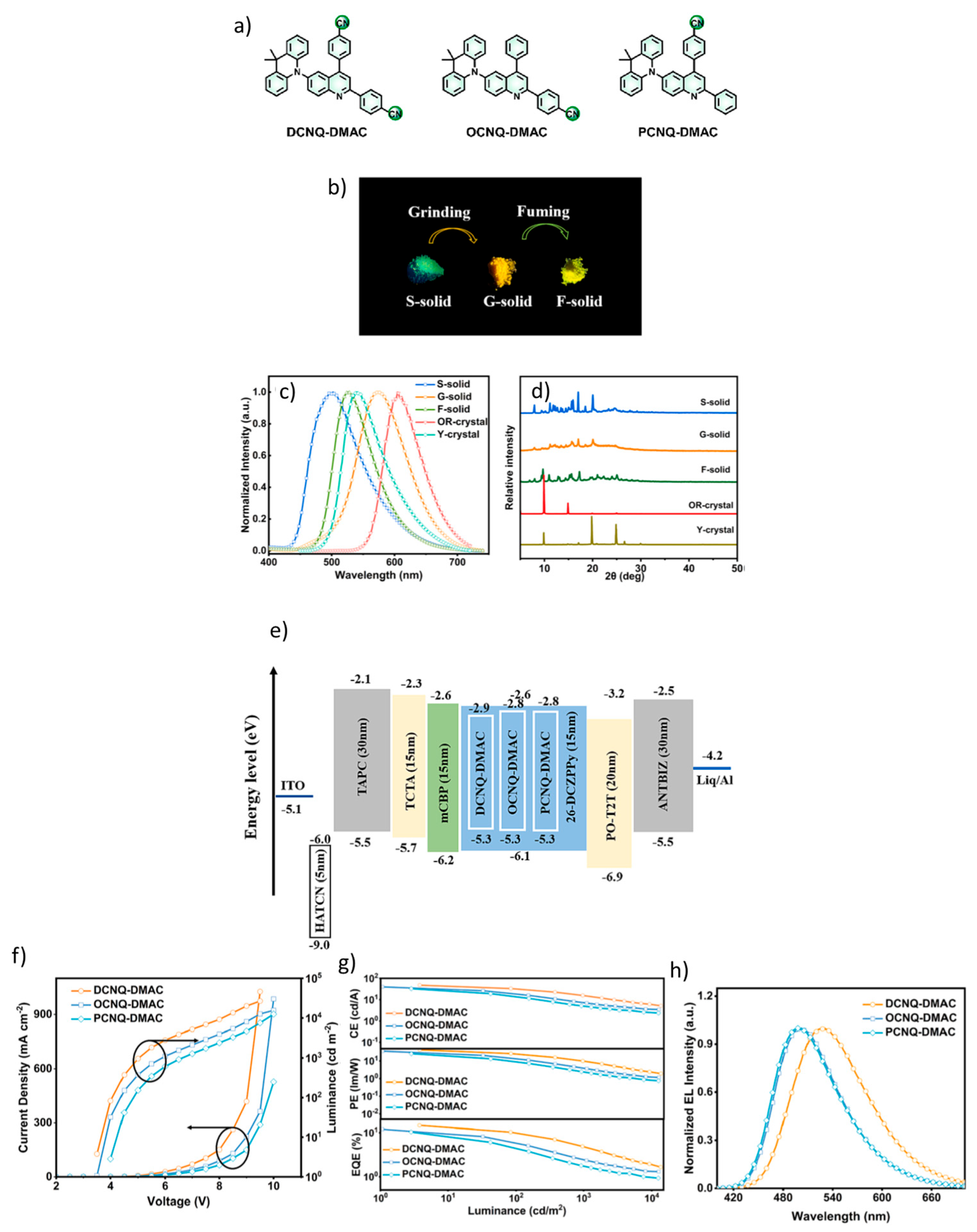
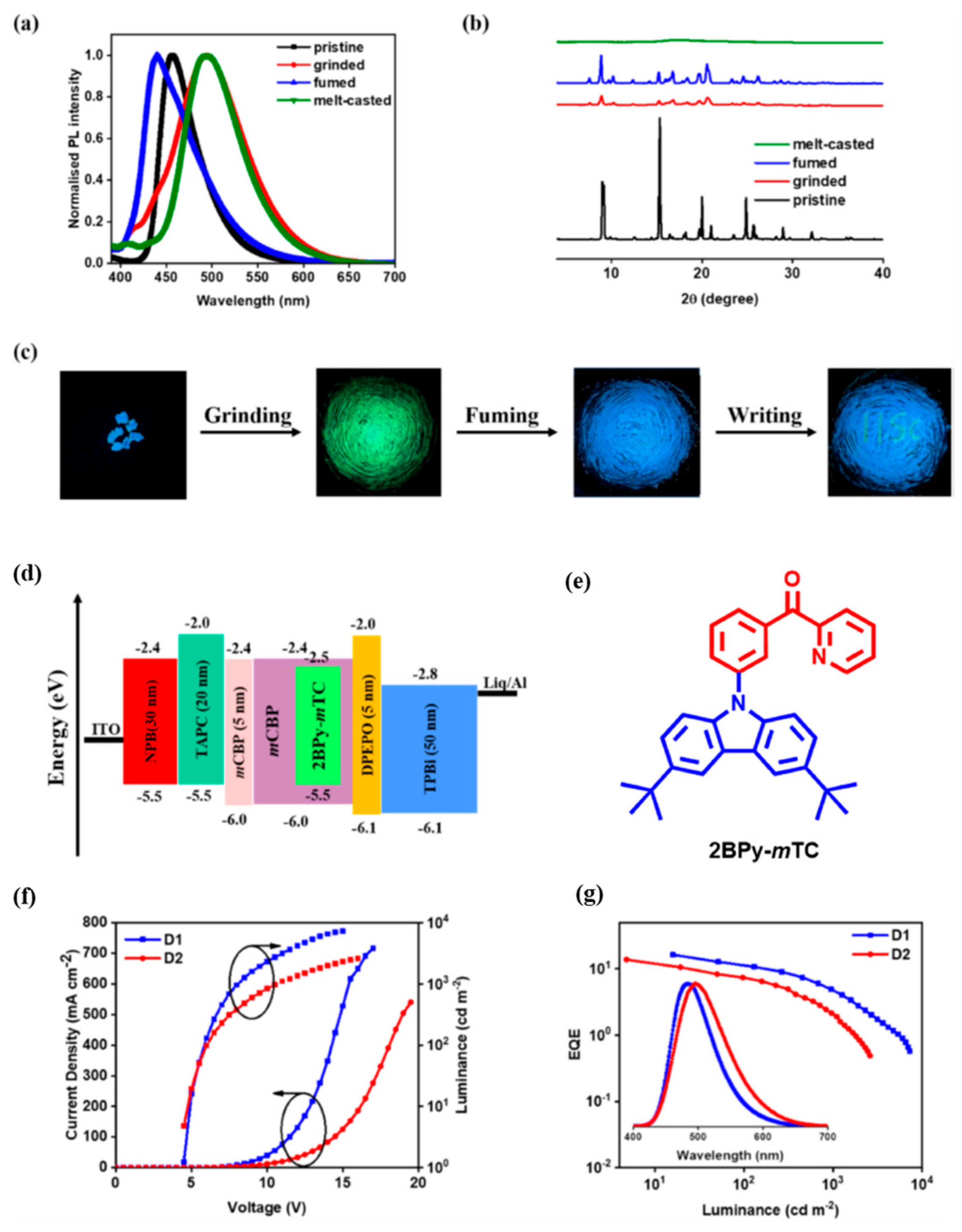
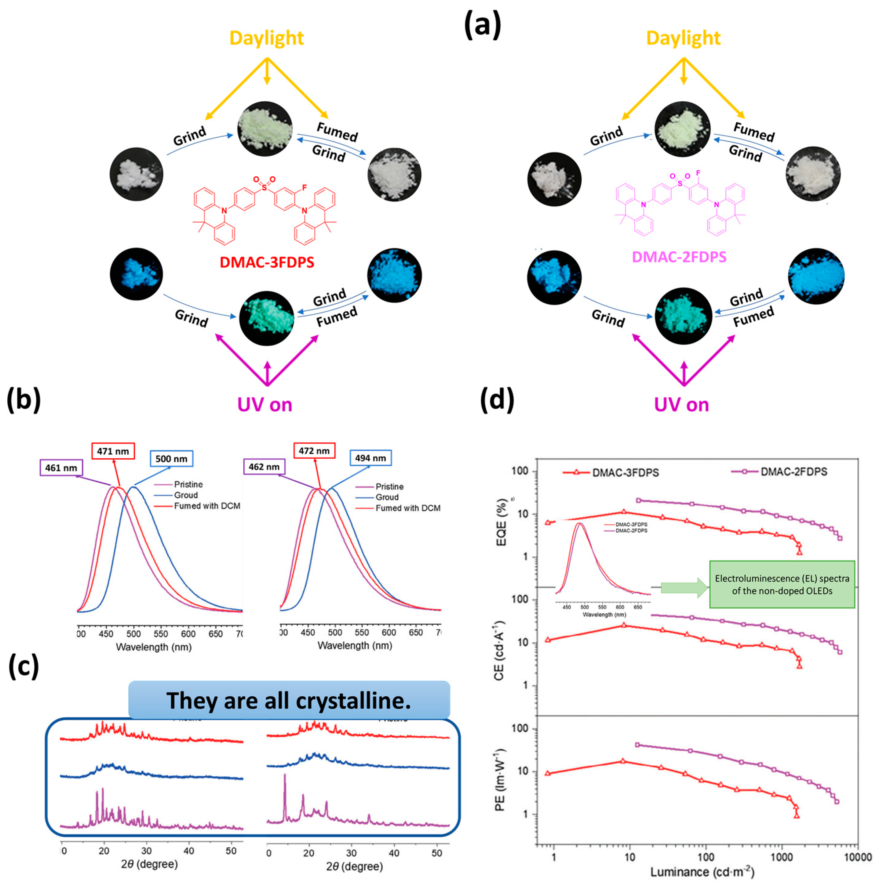
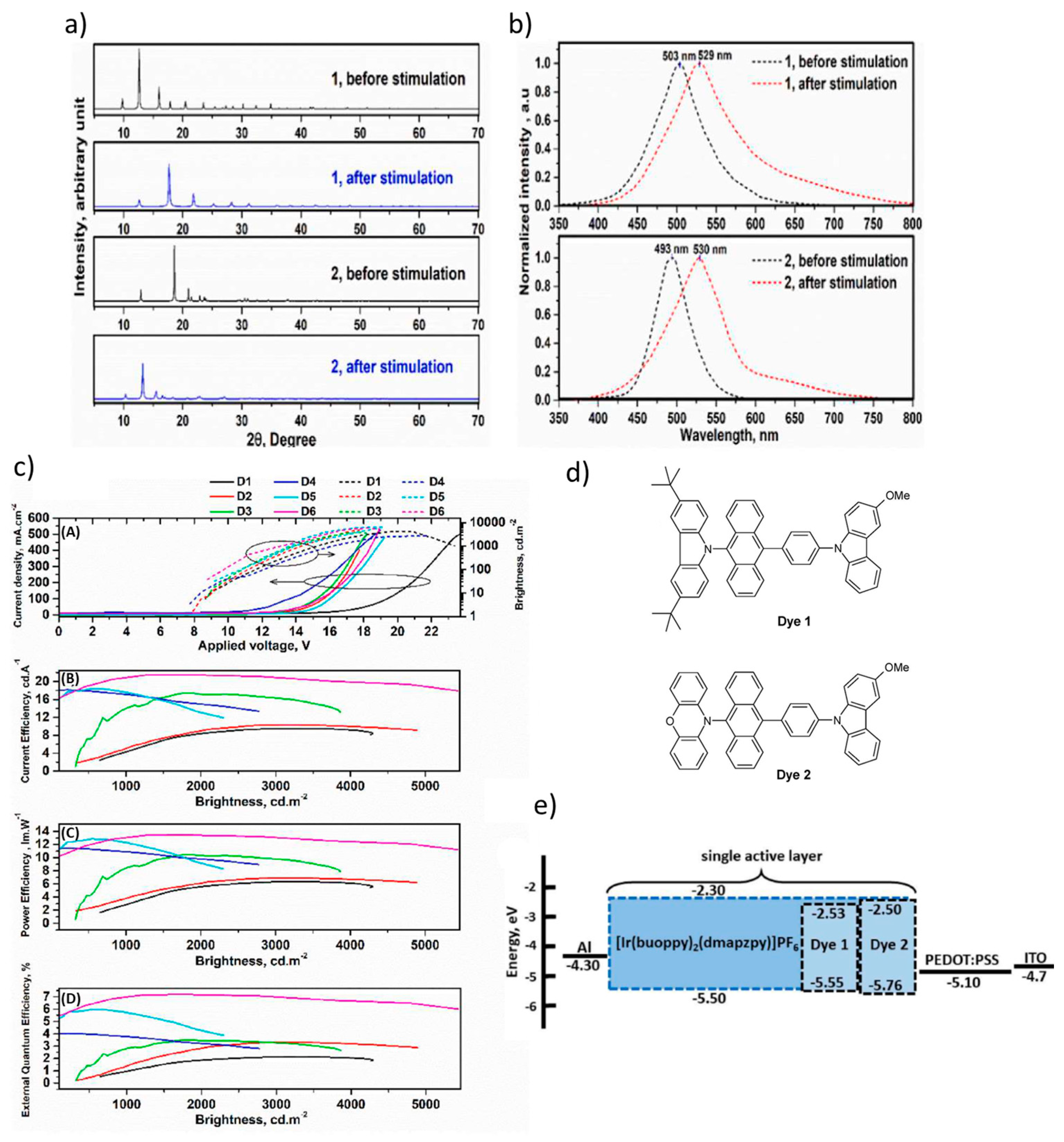
2.4. Integration of TADF and Mechanochromic Materials in OLEDs and LECs
3. Conclusions
Funding
Data Availability Statement
Conflicts of Interest
References
- Nakanotani, H.; Tsuchiya, Y.; Adachi, C. Thermally-activated Delayed Fluorescence for Light-emitting Devices. Chem. Lett. 2021, 50, 938–948. [Google Scholar] [CrossRef]
- Dias, F.B.; Bourdakos, K.N.; Jankus, V.; Moss, K.C.; Kamtekar, K.T.; Bhalla, V.; Santos, J.; Bryce, M.R.; Monkman, A.P. Triplet Harvesting with 100% Efficiency by Way of Thermally Activated Delayed Fluorescence in Charge Transfer OLED Emitters. Adv. Mater. 2013, 25, 3707–3714. [Google Scholar] [CrossRef] [PubMed]
- Zhao, K.; Zhao, Y.; Qian, R.; Ye, C.; Song, Y. Recent Advances in Interactive Mechanosensory Electronics with Luminescence/Coloration Outputs for Wearable Applications. ACS Mater. Lett. 2023, 5, 3093–3116. [Google Scholar] [CrossRef]
- Weder, C. Mechanochromic Polymers. In Encyclopedia of Polymeric Nanomaterials; Springer: Berlin/Heidelberg, Germany, 2013; pp. 1–11. [Google Scholar] [CrossRef]
- Dos Santos, J.M.; Hall, D.; Basumatary, B.; Bryden, M.; Chen, D.; Choudhary, P.; Comerford, T.; Crovini, E.; Danos, A.; De, J.; et al. The Golden Age of Thermally Activated Delayed Fluorescence Materials: Design and Exploitation. Chem. Rev. 2024, 124, 13736–14110. [Google Scholar] [CrossRef] [PubMed]
- Arano-Martinez, J.A.; Martínez-González, C.L.; Salazar, M.I.; Torres-Torres, C. A Framework for Biosensors Assisted by Multiphoton Effects and Machine Learning. Biosensors 2022, 12, 710. [Google Scholar] [CrossRef]
- Tang, S.; Santos, J.M.D.; Ràfols-Ribé, J.; Wang, J.; Zysman-Colman, E.; Edman, L. Introducing MR-TADF Emitters into Light-Emitting Electrochemical Cells for Narrowband and Efficient Emission. Adv. Funct. Mater. 2023, 33, 2306170. [Google Scholar] [CrossRef]
- Lee, C.W.; Lee, J.Y. Systematic Control of Photophysical Properties of Host Materials for High Quantum Efficiency above 25% in Green Thermally Activated Delayed Fluorescent Devices. ACS Appl. Mater. Interfaces 2015, 7, 2899–2904. [Google Scholar] [CrossRef]
- Shen, Y.; Kuddes, D.D.; Naquin, C.A.; Hesterberg, T.W.; Kusmierz, C.; Holliday, B.J.; Slinker, J.D. Improving light-emitting electrochemical cells with ionic additives. Appl. Phys. Lett. 2013, 102, 203305. [Google Scholar] [CrossRef]
- Yang, Z.; Mao, Z.; Xie, Z.; Zhang, Y.; Liu, S.; Zhao, J.; Xu, J.; Chi, Z.; Aldred, M.P. Recent advances in organic thermally activated delayed fluorescence materials. Chem. Soc. Rev. 2017, 46, 915–1016. [Google Scholar] [CrossRef]
- Pei, Q.; Yang, Y.; Yu, G.; Zhang, C.; Heeger, A.J. Polymer Light-Emitting Electrochemical Cells: In Situ Formation of a Light-Emitting p-n Junction. J. Am. Chem. Soc. 1996, 118, 3922–3929. [Google Scholar] [CrossRef]
- Gets, D.; Alahbakhshi, M.; Mishra, A.; Haroldson, R.; Papadimitratos, A.; Ishteev, A.; Saranin, D.; Anoshkin, S.; Pushkarev, A.; Danilovskiy, E.; et al. Reconfigurable Perovskite LEC: Effects of Ionic Additives and Dual Function Devices. Adv. Opt. Mater. 2021, 9, 2001715. [Google Scholar] [CrossRef]
- Giordano, F.; Abate, A.; Correa Baena, J.P.; Saliba, M.; Matsui, T.; Im, S.H.; Zakeeruddin, S.M.; Nazeeruddin, M.K.; Hagfeldt, A.; Graetzel, M. Enhanced electronic properties in mesoporous TiO2 via lithium doping for high-efficiency perovskite solar cells. Nat. Commun. 2016, 7, 10379. [Google Scholar] [CrossRef]
- Tang, S.; Tan, W.-Y.; Zhu, X.-H.; Edman, L. Small-molecule light-emitting electrochemical cells: Evidence for in situ electrochemical doping and functional operation. Chem. Commun. 2013, 49, 4926. [Google Scholar] [CrossRef]
- Wu, T.; Zeng, Q.; Zhu, Y.; Chen, H.; Shan, G.; Guo, T.; Hu, H.; Li, F. Enhancing the Performance of Light-Emitting Electrochemical Cells by Incorporating Quantum Dots. IEEE Trans. Electron. Devices 2024, 71, 3998–4001. [Google Scholar] [CrossRef]
- Lin, G.-R.; Cheng, J.-R.; Wang, C.-W.; Sarma, M.; Chen, H.-F.; Su, H.-C.; Chang, C.-H.; Wong, K.-T. Solid-state white light-emitting electrochemical cells based on scattering red color conversion layers. J. Mater. Chem. C Mater. 2015, 3, 12492–12498. [Google Scholar] [CrossRef]
- Mishra, A.; DiLuzio, S.; Alahbakhshi, M.; Adams, A.; Bowler, M.H.; Gu, Q.; Zakhidov, A.A.; Bernhard, S.; Slinker, J.D. Bright and Color-Tunable Single Layer Perovskite Host-Ionic Guest Light Emitting Electrochemical Cells. arXiv 2020, arXiv:2007.15455. [Google Scholar]
- Parker, S.T.; Slinker, J.D.; Lowry, M.S.; Cox, M.P.; Bernhard, S.; Malliaras, G.G. Improved turn-on times of iridium electroluminescent devices by use of ionic liquids. Chem. Mater. 2005, 17, 3187–3190. [Google Scholar] [CrossRef]
- Fresta, E.; Costa, R.D. Beyond traditional light-emitting electrochemical cells-a review of new device designs and emitters. R. Soc. Chem. 2017, 5, 5643–5675. [Google Scholar] [CrossRef]
- Tang, S.; Edman, L. Light-Emitting Electrochemical Cells: A Review on Recent Progress; Springer: Berlin/Heidelberg, Germany, 2016. [Google Scholar] [CrossRef]
- Liu, D.; Li, S.; Zhang, P.; Wang, Y.; Zhang, R.; Sarvari, H.; Wang, F.; Wu, J.; Wang, Z.; Chen, Z.D. Efficient planar heterojunction perovskite solar cells with Li-doped compact TiO2 layer. Nano Energy 2017, 31, 462–468. [Google Scholar] [CrossRef]
- Yu, Z.; Wang, M.; Lei, G.; Liu, J.; Li, L.; Pei, Q. Stabilizing the Dynamic p–i–n Junction in Polymer Light-Emitting Electrochemical Cells. J. Phys. Chem. Lett. 2011, 2, 367–372. [Google Scholar] [CrossRef]
- Dumur, F. Light-emitting electrochemical cells. In Luminescence in Electrochemistry: Applications in Analytical Chemistry, Physics and Biology; Springer International Publishing: Berlin/Heidelberg, Germany, 2016; pp. 327–361. [Google Scholar] [CrossRef]
- Hoke, E.T.; Slotcavage, D.J.; Dohner, E.R.; Bowring, A.R.; Karunadasa, H.I.; McGehee, M.D. Reversible photo-induced trap formation in mixed-halide hybrid perovskites for photovoltaics. Chem. Sci. 2015, 6, 613–617. [Google Scholar] [CrossRef] [PubMed]
- Smith, E.C.; Ellis, C.L.C.; Javaid, H.; Renna, L.A.; Liu, Y.; Russell, T.P.; Bag, M.; Venkataraman, D. Interplay between Ion Transport, Applied Bias, and Degradation under Illumination in Hybrid Perovskite p-i-n Devices. J. Phys. Chem. C 2018, 122, 13986–13994. [Google Scholar] [CrossRef]
- Eames, C.; Frost, J.M.; Barnes, P.R.F.; O’Regan, B.C.; Walsh, A.; Islam, M.S. Ionic transport in hybrid lead iodide perovskite solar cells. Nat. Commun. 2015, 6, 7497. [Google Scholar] [CrossRef] [PubMed]
- Yang, W.; Su, R.; Luo, D.; Hu, Q.; Zhang, F.; Xu, Z.; Wang, Z.; Tang, J.; Lv, Z.; Yang, X.; et al. Surface modification induced by perovskite quantum dots for triple-cation perovskite solar cells. Nano Energy 2020, 67, 104189. [Google Scholar] [CrossRef]
- Tiguntseva, E.Y.; Baranov, D.G.; Pushkarev, A.P.; Munkhbat, B.; Komissarenko, F.; Franckevičius, M.; Zakhidov, A.A.; Shegai, T.; Kivshar, Y.S.; Makarov, S.V. Tunable Hybrid Fano Resonances in Halide Perovskite Nanoparticles. Nano Lett. 2018, 18, 5522–5529. [Google Scholar] [CrossRef]
- Futscher, M.H.; Lee, J.M.; McGovern, L.; Muscarella, L.A.; Wang, T.; Haider, M.I.; Fakharuddin, A.; Schmidt-Mende, L.; Ehrler, B. Quantification of ion migration in CH3NH3PbI3 perovskite solar cells by transient capacitance measurements. Mater. Horiz. 2019, 6, 1497–1503. [Google Scholar] [CrossRef]
- Frost, J.M.; Butler, K.T.; Brivio, F.; Hendon, C.H.; van Schilfgaarde, M.; Walsh, A. Atomistic Origins of High-Performance in Hybrid Halide Perovskite Solar Cells. Nano Lett. 2014, 14, 2584–2590. [Google Scholar] [CrossRef]
- Yuan, Y.; Huang, J. Ion Migration in Organometal Trihalide Perovskite and Its Impact on Photovoltaic Efficiency and Stability. Acc. Chem. Res. 2016, 49, 286–293. [Google Scholar] [CrossRef]
- Domanski, K.; Roose, B.; Matsui, T.; Saliba, M.; Turren-Cruz, S.-H.; Correa-Baena, J.-P.; Carmona, C.R.; Richardson, G.; Foster, J.M.; De Angelis, F.; et al. Migration of cations induces reversible performance losses over day/night cycling in perovskite solar cells. Energy Environ. Sci. 2017, 10, 604–613. [Google Scholar] [CrossRef]
- Xiao, Z.; Yuan, Y.; Shao, Y.; Wang, Q.; Dong, Q.; Bi, C.; Sharma, P.; Gruverman, A.; Huang, J. Giant switchable photovoltaic effect in organometal trihalide perovskite devices. Nat. Mater. 2015, 14, 193–198. [Google Scholar] [CrossRef]
- Deng, Y.; Xiao, Z.; Huang, J. Light-Induced Self-Poling Effect on Organometal Trihalide Perovskite Solar Cells for Increased Device Efficiency and Stability. Adv. Energy Mater. 2015, 5, 1500721. [Google Scholar] [CrossRef]
- Gets, D.; Saranin, D.; Ishteev, A.; Haroldson, R.; Danilovskiy, E.; Makarov, S.; Zakhidov, A. Light-emitting perovskite solar cell with segregation enhanced self doping. Appl. Surf. Sci. 2019, 476, 486–492. [Google Scholar] [CrossRef]
- Yuan, Y.; Li, T.; Wang, Q.; Xing, J.; Gruverman, A.; Huang, J. Anomalous photovoltaic effect in organic-inorganic hybrid perovskite solar cells. Sci. Adv. 2017, 3, e1602164. [Google Scholar] [CrossRef] [PubMed]
- Katsumata, J.; Osawa, F.; Sato, G.; Sato, A.; Miwa, K.; Ono, S.; Marumoto, K. Investigating the operation mechanism of light-emitting electrochemical cells through operando observations of spin states. Commun. Mater. 2023, 4, 41. [Google Scholar] [CrossRef]
- Operating Mechanism of Light-Emitting Electrochemical Cells. 1996. Available online: www.nature.com/naturematerials (accessed on 25 November 2024).
- Meier, S.B.; Tordera, D.; Pertegás, A.; Roldán-Carmona, C.; Ortí, E.; Bolink, H.J. Light-Emitting Electrochemical Cells: Recent Progress and Future Prospects; Elsevier: Amsterdam, The Netherlands, 2014. [Google Scholar] [CrossRef]
- Saranin, D.S.; Muratov, D.S.; Haroldson, R.; Nasibulin, A.G.; Ishteev, A.R.; Kuznetsov, D.V.; Orlova, M.N.; Didenko, S.I.; Zakhidov, A.A. Ionically gated perovskite solar cell with tunable carbon nanotube interface at thick fullerene electron transporting layer: Comparison to gated OPV. arXiv 2019, arXiv:1911.02619. [Google Scholar]
- Ishteev, A.; Haroldson, R.; Gets, D.; Tsapenko, A.; Alahbakhshi, M.; Moon, J.; Martinez, P.; Usupov, K.; Nasibulin, A.; Makarov, S.; et al. Ambipolar perovskite light electrochemical cell for transparent display devices. arXiv 2019, arXiv:1911.06875. [Google Scholar]
- Gets, D.S.; Verkhogliadov, G.A.; Danilovskiy, E.Y.; Baranov, A.I.; Makarov, S.V.; Zakhidov, A.A. Dipolar cation accumulation at the interfaces of perovskite light-emitting solar cells. J. Mater. Chem. C Mater. 2020, 8, 16992–16999. [Google Scholar] [CrossRef]
- Mishra, A.; Alahbakhshi, M.; Haroldson, R.; Bastatas, L.D.; Gu, Q.; Zakhidov, A.A.; Slinker, J.D. Enhanced Operational Stability of Perovskite Light-Emitting Electrochemical Cells Leveraging Ionic Additives. Adv. Opt. Mater. 2020, 8, 2000226. [Google Scholar] [CrossRef]
- Baldo, M.A.; O’Brien, D.F.; You, Y.; Shoustikov, A.; Sibley, S.; Thompson, M.E.; Forrest, S.R. Highly efficient phosphorescent emission from organic electroluminescent devices. Nature 1998, 395, 151–154. [Google Scholar] [CrossRef]
- Burroughes, J.H.; Bradley, D.D.C.; Brown, A.R.; Marks, R.N.; Mackay, K.; Friend, R.H.; Burns, P.L.; Holmes, A.B. Light-emitting diodes based on conjugated polymers. Nature 1990, 347, 539–541. [Google Scholar] [CrossRef]
- Forrest, S.R.; Baldo, M.A.; Brown, J.J.; D’Andrade, B.; Kawamura, Y.; Kwong, R.; Thompson, M.E.; Yanagida, S. Electrophosphorescent Organic Light Emitting Devices. SID Symp. Dig. Tech. Pap. 2002, 33, 1357–1359. [Google Scholar] [CrossRef]
- Tseng, Z.-L.; Huang, W.-L.; Yeh, T.-H.; Xu, Y.-X.; Chiang, C.-H. Thermally Activated Delayed Fluorescence in Commercially Available Materials for Solution-Process Exciplex OLEDs. Polymers 2021, 13, 1668. [Google Scholar] [CrossRef] [PubMed]
- Son, S.; Yoon, S.; Jang, J.; Kang, M.; Jeon, S. Pure Aluminum Metal as an Anode for High Performance OLEDs. SID Symp. Dig. Tech. Pap. 2004, 35, 52–53. [Google Scholar] [CrossRef]
- Yersin, H. Highly Efficient OLEDs: Materials Based on Thermally Activated Delayed Fluorescence; Wiley-VCH: Hoboken, NJ, USA, 2019. [Google Scholar]
- Goushi, K.; Yoshida, K.; Sato, K.; Adachi, C. Organic light-emitting diodes employing efficient reverse intersystem crossing for triplet-to-singlet state conversion. Nat. Photonics 2012, 6, 253–258. [Google Scholar] [CrossRef]
- Yadav, R.A.K.; Dubey, D.K.; Chen, S.-Z.; Liang, T.-W.; Jou, J.-H. Role of Molecular Orbital Energy Levels in OLED Performance. Sci. Rep. 2020, 10, 9915. [Google Scholar] [CrossRef]
- Cebrián, C.; Mauro, M. Recent advances in phosphorescent platinum complexes for organic light-emitting diodes. Beilstein J. Org. Chem. 2018, 14, 1459–1481. [Google Scholar] [CrossRef]
- Mao, H.-T.; Li, G.-F.; Shan, G.-G.; Wang, X.-L.; Su, Z.-M. Recent progress in phosphorescent Ir(III) complexes for nondoped organic light-emitting diodes. Coord. Chem. Rev. 2020, 413, 213283. [Google Scholar] [CrossRef]
- Zhan, L.; Chen, Z.; Gong, S.; Xiang, Y.; Ni, F.; Zeng, X.; Xie, G.; Yang, C. A Simple Organic Molecule Realizing Simultaneous TADF, RTP, AIE, and Mechanoluminescence: Understanding the Mechanism Behind the Multifunctional Emitter. Angew. Chem. Int. Ed. 2019, 58, 17651–17655. [Google Scholar] [CrossRef]
- Wong, M.Y.; Zysman-Colman, E. Purely Organic Thermally Activated Delayed Fluorescence Materials for Organic Light-Emitting Diodes. Adv. Mater. 2017, 29, 1605444. [Google Scholar] [CrossRef]
- Kido, J.; Kimura, M.; Nagai, K. Multilayer White Light-Emitting Organic Electroluminescent Device. Science 1995, 267, 1332–1334. [Google Scholar] [CrossRef]
- Li, X.-L.; Ouyang, X.; Liu, M.; Ge, Z.; Peng, J.; Cao, Y.; Su, S.-J. Highly efficient single- and multi-emission-layer fluorescent/phosphorescent hybrid white organic light-emitting diodes with ~20% external quantum efficiency. J. Mater. Chem. C Mater. 2015, 3, 9233–9239. [Google Scholar] [CrossRef]
- Sun, Y.; Giebink, N.C.; Kanno, H.; Ma, B.; Thompson, M.E.; Forrest, S.R. Management of singlet and triplet excitons for efficient white organic light-emitting devices. Nature 2006, 440, 908–912. [Google Scholar] [CrossRef] [PubMed]
- Reineke, S.; Lindner, F.; Schwartz, G.; Seidler, N.; Walzer, K.; Lüssem, B.; Leo, K. White organic light-emitting diodes with fluorescent tube efficiency. Nature 2009, 459, 234–238. [Google Scholar] [CrossRef]
- Yoshida, H.; Yoshizaki, K. Electron affinities of organic materials used for organic light-emitting diodes: A low-energy inverse photoemission study. Org. Electron. 2015, 20, 24–30. [Google Scholar] [CrossRef]
- Kippelen, B.; Brédas, J.-L. Organic photovoltaics. Energy Environ. Sci. 2009, 2, 251. [Google Scholar] [CrossRef]
- Höfle, S.; Lutz, T.; Egel, A.; Nickel, F.; Kettlitz, S.W.; Gomard, G.; Lemmer, U.; Colsmann, A. Influence of the Emission Layer Thickness on the Optoelectronic Properties of Solution Processed Organic Light-Emitting Diodes. ACS Photonics 2014, 1, 968–973. [Google Scholar] [CrossRef]
- Kirch, A.; Park, S.-R.; Ràfols-Ribé, J.; Kassel, J.A.; Zhang, X.; Tang, S.; Larsen, C.; Edman, L. Impact of the Electrode Material on the Performance of Light-Emitting Electrochemical Cells. ACS Appl. Mater. Interfaces 2025, 17, 5184–5192. [Google Scholar] [CrossRef]
- Shao, Y.; Bazan, G.C.; Heeger, A.J. Long-Lifetime Polymer Light-Emitting Electrochemical Cells. Adv. Mater. 2007, 19, 365–370. [Google Scholar] [CrossRef]
- Matyba, P.; Maturova, K.; Kemerink, M.; Robinson, N.D.; Edman, L. The dynamic organic p–n junction. Nat. Mater. 2009, 8, 672–676. [Google Scholar] [CrossRef]
- Adachi, C.; Xie, G.; Reineke, S.; Zysman-Colman, E. Recent Advances in Thermally Activated Delayed Fluorescence Materials. Front. Chem. 2020, 8, 625910. [Google Scholar] [CrossRef]
- Liu, Y.; Hangoma, P.M.; Tamilavan, V.; Shin, I.; Hwang, I.W.; Jung, Y.K.; Kim, K.H. Dual-functional light-emitting perovskite solar cells enabled by soft-covered annealing process. Nano Energy 2019, 61, 251–258. [Google Scholar] [CrossRef]
- Gil-Escrig, L.; Longo, G.; Pertegás, A.; Roldán-Carmona, C.; Soriano, A.; Sessolo, M.; Bolink, H.J. Efficient photovoltaic and electroluminescent perovskite devices. Chem. Commun. 2015, 51, 569–571. [Google Scholar] [CrossRef] [PubMed]
- Li, S.; Yang, Z.; Xie, Y.; Hua, L.; Ying, S.; Liu, Y.; Ren, Z.; Yan, S. Modulatory spin-flip of triplet excitons via diversiform electron-donating units for MR-TADF emitters towards solution-processed narrowband OLEDs. Chem. Sci. 2024, 15, 18335–18346. [Google Scholar] [CrossRef]
- Wang, J.; Tao, Y.; Wang, J.; Tao, Y. Benzonitrile/pyridylbenzoimidazole hybrid electron-transport material for efficient phosphorescence and TADF OLEDs. Mater. Lett. 2024, 356, 135624. [Google Scholar] [CrossRef]
- Zhang, K.; Zhang, W.; Cao, Q.; Zhou, T.; Ge, F.; Xu, H.; Wang, J.; Ban, X.; Zhang, T. Turning the energy channel of side-chain TADF polymers by monomer optimization for high-efficiency solution-processed white OLEDs. J. Lumin. 2023, 263, 119966. [Google Scholar] [CrossRef]
- Van Reenen, S.; Matyba, P.; Dzwilewski, A.; Janssen, R.A.J.; Edman, L.; Kemerink, M. A unifying model for the operation of light-emitting electrochemical cells. J. Am. Chem. Soc. 2010, 132, 13776–13781. [Google Scholar] [CrossRef]
- Lee, Y.H.; Lee, W.; Lee, T.; Jung, J.; Yoo, S.; Lee, M.H. Achieving over 36% EQE in blue OLEDs using rigid TADF emitters based on spiro-donor and spiro-B-heterotriangulene acceptors. Chem. Eng. J. 2023, 452, 139387. [Google Scholar] [CrossRef]
- Zhang, T.; Xiao, Y.; Wang, H.; Kong, S.; Huang, R.; Ka-Man Au, V.; Yu, T.; Huang, W. Highly Twisted Thermally Activated Delayed Fluorescence (TADF) Molecules and Their Applications in Organic Light-Emitting Diodes (OLEDs). Angew. Chem. Int. Ed. 2023, 62, 139387. [Google Scholar] [CrossRef]
- Hua, T.; Liu, Y.-C.; Huang, C.-W.; Li, N.; Zhou, C.; Huang, Z.; Cao, X.; Wu, C.-C.; Yang, C. High-efficiency and low roll-off deep-blue OLEDs enabled by thermally activated delayed fluorescence emitter with preferred horizontal dipole orientation. Chem. Eng. J. 2022, 433, 133598. [Google Scholar] [CrossRef]
- Nasiri, S.; Rabiei, M.; Shaki, H.; Hosseinnezhad, M.; Kalyani, K.; Palevicius, A.; Vilkauskas, A.; Janusas, G.; Nutalapati, V.; Kment, S.; et al. What is TADF (thermally activated delayed fluorescence) compared to the mechanisms of FL (fluorescence), PH (phosphorescence), and TTA (triplet–triplet annihilation) based on a novel naphthalimide sulfonylphenyl derivative as a host? J. Photochem. Photobiol. A Chem. 2024, 447, 115289. [Google Scholar] [CrossRef]
- Kang, I.B.; Han, C.W.; Kyeong, J.; Editors, J. Series in Display Science and Technology Advanced Display Technology Next Generation Self-Emitting Displays. Available online: http://www.springer.com/series/15379 (accessed on 6 February 2025).
- Liu, Q.; Chen, W.-C.; Zhang, R.; Wei, H.; Liu, B.; Jin, J.-M.; Liu, Y.; Ye, Z.; Chen, J.-X.; Ji, S.; et al. Design, synthesis, and electroluminescence of red TADF dyes based on cyanophenanthrene. Dye. Pigments 2023, 212, 111125. [Google Scholar] [CrossRef]
- Endo, A.; Ogasawara, M.; Takahashi, A.; Yokoyama, D.; Kato, Y.; Adachi, C. Thermally activated delayed fluorescence from Sn4+-porphyrin complexes and their application to organic light-emitting diodes—A novel mechanism for electroluminescence. Adv. Mater. 2009, 21, 4802–4806. [Google Scholar] [CrossRef] [PubMed]
- Fatahi, M.; Chen, D.; Zysman-Colman, E. Blue Emission in Sterically Shielded Multiresonant Thermally Activated Delayed Fluorescence Emitters. ChemRxiv 2025. [Google Scholar] [CrossRef]
- Bui, T.T.; Goubard, F.; Ibrahim-Ouali, M.; Gigmes, D.; Dumur, F. Recent advances on organic blue thermally activated delayed fluorescence (TADF) emitters for organic light-emitting diodes (OLEDs). Beilstein J. Org. Chem. 2018, 30, 282–308. [Google Scholar] [CrossRef]
- Aizawa, N.; Vázquez, R.J. Thermally Activated Delayed Fluorescence (TADF) Active Systems: Mechanism, Applications, and Future Directions. J. Phys. Chem. C 2025, 129, 3359–3360. [Google Scholar] [CrossRef]
- Yao, H.; Zhang, Y.; Wang, G.; Li, J.; Huang, J.; Wang, X.; Zhang, Z.; Chen, L.; Pan, Z.; Zhang, K. TADF-Type Organic Afterglow Nanoparticles with Temperature and Oxygen Dual-Responsive Property for Bimodal Sensing. ACS Appl. Nano Mater. 2023, 6, 15138–15146. [Google Scholar] [CrossRef]
- Pander, P.; Dias, F.B. Photophysical Characterisation of Thermally Activated Delayed Fluorescence (TADF) Materials. Disp. Imaging 2017, 2, 249–263. [Google Scholar]
- Zhao, K.; Omar, Ö.H.; Nematiaram, T.; Padula, D.; Troisi, A. Novel thermally activated delayed fluorescence materials by high-throughput virtual screening: Going beyond donor–acceptor design. J. Mater. Chem. C Mater. 2021, 9, 3324–3333. [Google Scholar] [CrossRef]
- Liu, F.-M.; Ding, L.-Y.; Yu, Y.-J.; Li, M.-T.; Liao, L.-S.; Jiang, Z.-Q. Toward narrowband emission: The chemical strategies for modifying boron-based luminescent materials. J. Mater. Chem. C Mater. 2023, 11, 11425–11439. [Google Scholar] [CrossRef]
- Hong, X.; Zhang, D.; Yin, C.; Wang, Q.; Zhang, Y.; Huang, T.; Wei, J.; Zeng, X.; Meng, G.; Wang, X.; et al. TADF molecules with π-extended acceptors for simplified high-efficiency blue and white organic light-emitting diodes. Chemistry 2022, 8, 1705–1719. [Google Scholar] [CrossRef]
- Liu, W.; Pan, J.; Sun, Q.; Dai, Y.; Yang, D.; Qiao, X.; Ma, D. Exciton dynamics of the efficiency roll-off of exciplex-based OLEDs and low efficiency roll-off phosphorescence OLEDs based on an exciplex as the host. J. Mater. Chem. C Mater. 2024, 12, 12317–12324. [Google Scholar] [CrossRef]
- Crucho, C.I.C.; Avó, J.; Diniz, A.M.; Pinto, S.N.; Barbosa, J.; Smith, P.O.; Berberan-Santos, M.N.; Pålsson, L.-O.; Dias, F.B. TADF Dye-Loaded Nanoparticles for Fluorescence Live-Cell Imaging. Front. Chem. 2020, 8, 404. [Google Scholar] [CrossRef] [PubMed]
- Valchanov, G.; Ivanova, A.; Tadjer, A.; Chercka, D.; Baumgarten, M. Understanding the Fluorescence of TADF Light-Emitting Dyes. J. Phys. Chem. A 2016, 120, 6944–6955. [Google Scholar] [CrossRef] [PubMed]
- Ferraro, V.; Bizzarri, C.; Bräse, S. Thermally Activated Delayed Fluorescence (TADF) Materials Based on Earth-Abundant Transition Metal Complexes: Synthesis, Design and Applications; John Wiley and Sons Inc.: Hoboken, NJ, USA, 2024. [Google Scholar] [CrossRef]
- Chen, D.; Wang, H.; Sun, D.; Wu, S.; Wang, K.; Zhang, X.; Zysman-Colman, E. The combination of a donor-acceptor thermally activated delayed fluorescence moiety (TADF) and a multiresonant (MR-TADF) emitting core results in outstanding electroluminescence performance. ChemRxiv 2024. [Google Scholar] [CrossRef]
- Shi, Y.-Z.; Wu, H.; Wang, K.; Yu, J.; Ou, X.-M.; Zhang, X.-H. Recent progress in thermally activated delayed fluorescence emitters for nondoped organic light-emitting diodes. Chem. Sci. 2022, 13, 3625–3651. [Google Scholar] [CrossRef]
- Tang, C. Fundamental Aspects of Stretchable Mechanochromic Materials: Fabrication and Characterization. Materials 2024, 17, 3980. [Google Scholar] [CrossRef]
- Lötzsch, D.; Eberhardt, V.; Rabe, C. Chromogenic Materials. In Ullmann’s Encyclopedia of Industrial Chemistry; Wiley-VCH Verlag GmbH & Co. KGaA: Hoboken, NJ, USA, 2016; pp. 1–26. [Google Scholar] [CrossRef]
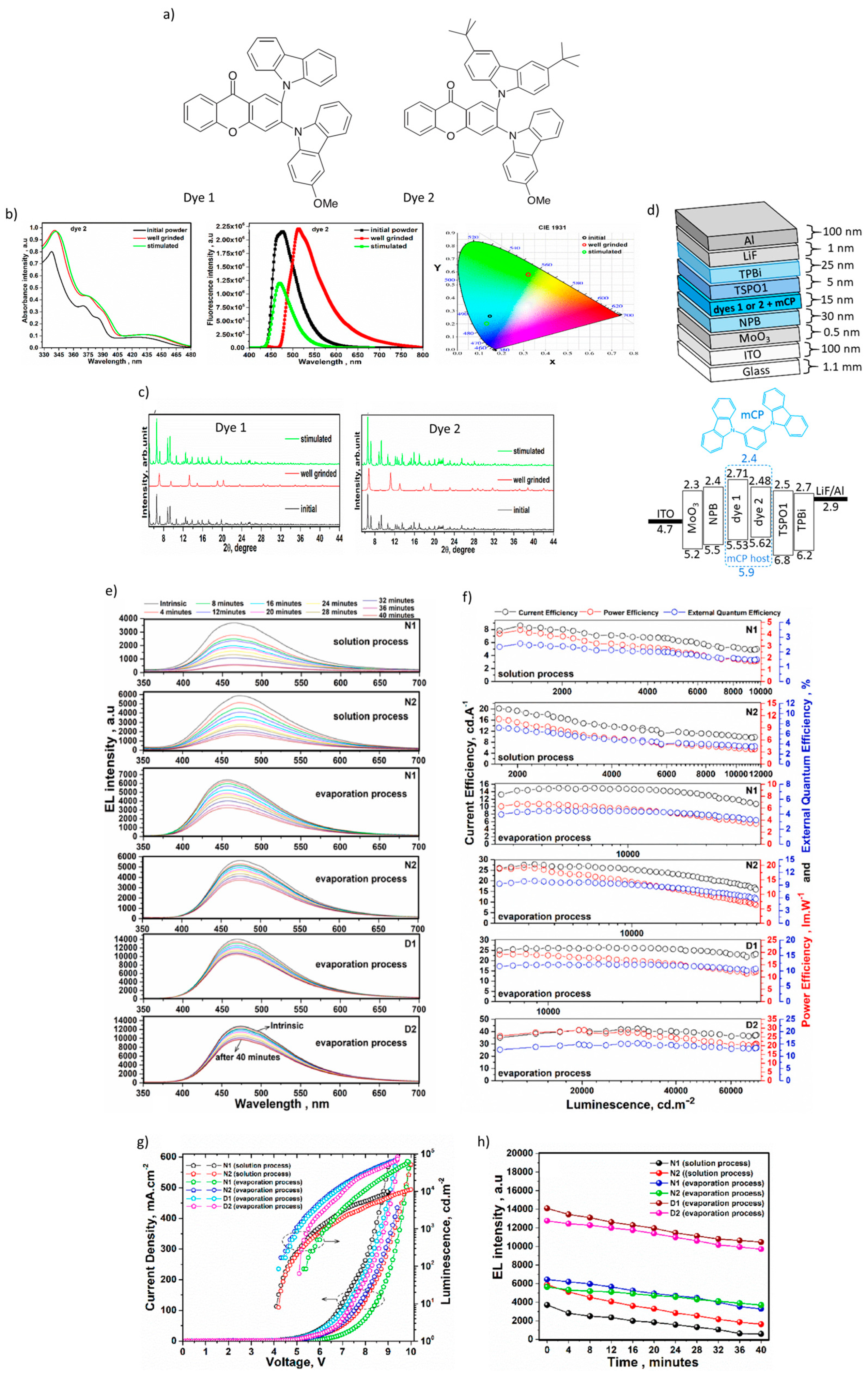
- Nasiri, S.; Dashti, A.; Hosseinnezhad, M.; Rabiei, M.; Palevicius, A.; Doustmohammadi, A.; Janusas, G. Mechanochromic and thermally activated delayed fluorescence dyes obtained from D–A–D′ type, consisted of xanthen and carbazole derivatives as an emitter layer in organic light emitting diodes. Chem. Eng. J. 2022, 430, 131877. [Google Scholar] [CrossRef]
- Mu, Y.; Liao, L.; Li, W.; Yang, Z.; Zhang, Y.; Huo, Y.; Chi, Z. Y-Shaped D-A Type Thioxanthone Derivatives: Mechano-Induced Thermally Activated Delayed Fluorescence and High-Contrast Mechano-Responsive Luminescence. Chem.—Eur. J. 2023, 29, e202300867. [Google Scholar] [CrossRef]
- Li, Z.; Liu, Y.; Marin, M.; Yin, Y. Thickness-dependent wrinkling of PDMS films for programmable mechanochromic responses. Nano Res. 2020, 13, 1882–1888. [Google Scholar] [CrossRef]
- Nasiri, S.; Hosseinnezhad, M.; Rabiei, M.; Palevicius, A.; Rahimi, Z.; Janusas, G.; Vilkauskas, A. New approach of mechanochromic, thermally activated delayed fluorescence’ dyes consisting of ‘thioxanthenone derivative as an acceptor unit and two carbazole derivatives as the donor units’ used as emitting layer in organic light-emitting diodes. Opt. Mater. 2022, 127, 112320. [Google Scholar] [CrossRef]
- Zhang, Z.; Wei, B.; Hu, Y.; Yang, D.; Ma, D.; Huang, S. Extraordinary sensitive mechanochromic hydrogels for visually detecting ultrasmall pressure. Cell Rep. Phys. Sci. 2023, 4, 101387. [Google Scholar] [CrossRef]
- Ito, S. Mechanochromic luminescence of soft crystals: Recent systematic studies in controlling the molecular packing and mechanoresponsive properties. J. Photochem. Photobiol. C Photochem. Rev. 2022, 51, 100481. [Google Scholar] [CrossRef]
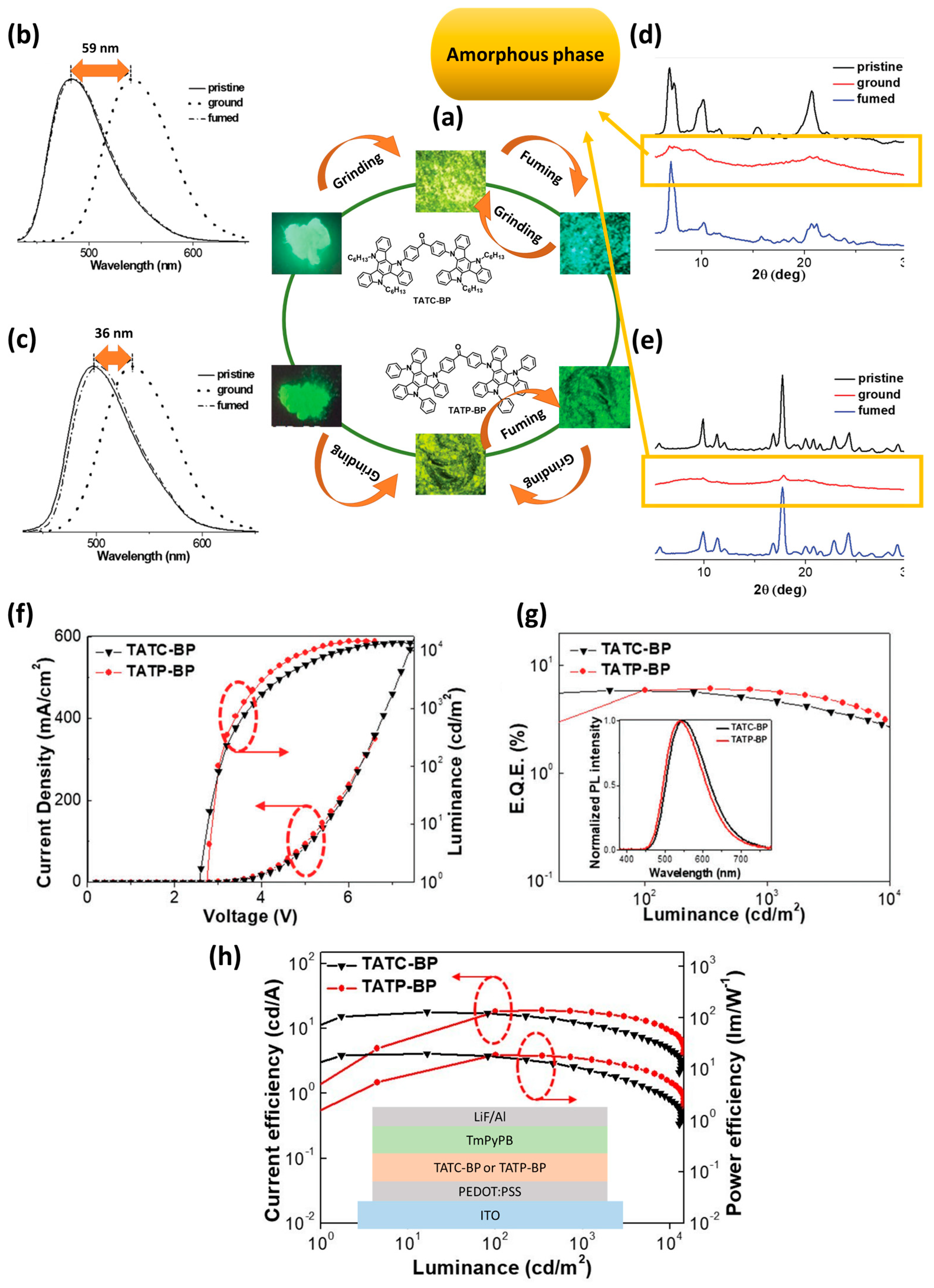
- Zeng, X.; Zhou, T.; Liu, J.; Wu, K.; Li, S.; Xiao, X.; Zhang, Y.; Gong, S.; Xie, G.; Yang, C. Incorporating Thermally Activated Delayed Fluorescence into Mechanochromic Luminescent Emitters: High-Performance Solution-Processed Yellow Organic Light Emitting Diodes. Adv. Opt. Mater. 2018, 6, 1801071. [Google Scholar] [CrossRef]
- Nasiri, S.; Hosseinnezhad, M.; Rabiei, M.; Palevicius, A.; Janusas, G.; Vilkauskas, A. Acceptor-phenyl-donor mechanochromic dyes based on 9-Bromoanthracene. J. Mol. Struct. 2023, 1278, 134953. [Google Scholar] [CrossRef]
- Xu, J.; Chi, Z. (Eds.) Mechanochromic Fluorescent Materials; Royal Society of Chemistry: Cambridge, UK, 2014. [Google Scholar] [CrossRef]
- Chen, Y.; Wang, S.; Wu, X.; Xu, Y.; Li, H.; Liu, Y.; Tong, H.; Wang, L. Triazatruxene-based small molecules with thermally activated delayed fluorescence, aggregation-induced emission and mechanochromic luminescence properties for solution-processable nondoped OLEDs. J. Mater. Chem. C Mater. 2018, 6, 12503–12508. [Google Scholar] [CrossRef]
- Zheng, K.; Yang, H.; Ni, F.; Chen, Z.; Gong, S.; Lu, Z.; Yang, C. Multifunctional Thermally Activated Delayed Fluorescence Emitters and Insight into Multicolor-Mechanochromism Promoted by Weak Intra- and Intermolecular Interactions. Adv. Opt. Mater. 2019, 7, 1900727. [Google Scholar] [CrossRef]
- Ganesan, P.; Ranganathan, R.; Chi, Y.; Liu, X.K.; Lee, C.S.; Liu, S.H.; Lee, G.H.; Lin, T.C.; Chen, Y.T.; Chou, P.T. Functional Pyrimidine-Based Thermally Activated Delay Fluorescence Emitters: Photophysics, Mechanochromism, and Fabrication of Organic Light-Emitting Diodes. Chem. Eur. J. 2017, 23, 2858–2866. [Google Scholar] [CrossRef]
- Kim, T.; Sohn, S.; Park, S.; Choi, W.; Ahn, H.; Jung, S.; Park, T. Intramolecular hydrogen bonding-induced conformation-locked multifunctional emitters for non-doped OLEDs. Chem. Eng. J. 2023, 478, 147444. [Google Scholar] [CrossRef]
- Hu, F.; Yang, W.; Li, L.; Miao, J.; Gong, S.; Ye, C.; Gao, X.; Yang, C. Multifunctional emitters with TADF, AIE, polymorphism and high-contrast multicolor mechanochromism: Efficient organic light-emitting diodes. Chem. Eng. J. 2023, 464, 142678. [Google Scholar] [CrossRef]
- Yadav, N.; Rajamalli, P. Multifunctional thermally activated delayed fluorescence emitter for both doped and non-doped organic light emitting diodes. Org. Electron. 2025, 136, 107157. [Google Scholar] [CrossRef]
- Ge, X.; Li, G.; Guo, D.; Yang, Z.; Mao, Z.; Zhao, J.; Chi, Z. A Strategy for Designing Multifunctional TADF Materials for High-Performance Non-doped OLEDs by Intramolecular Halogen Bonding. Adv. Opt. Mater. 2024, 12, 2302535. [Google Scholar] [CrossRef]
- Rajamalli, P.; Senthilkumar, N.; Gandeepan, P.; Ren-Wu, C.-Z.; Lin, H.-W.; Cheng, C.-H. A thermally activated delayed blue fluorescent emitter with reversible externally tunable emission. J. Mater. Chem. C Mater. 2016, 4, 900–904. [Google Scholar] [CrossRef]
- Sudhakar, P.; Gupta, A.K.; Cordes, D.B.; Zysman-Colman, E. Thermally activated delayed fluorescence emitters showing wide-range near-infrared piezochromism and their use in deep-red OLEDs. Chem. Sci. 2023, 15, 545–554. [Google Scholar] [CrossRef] [PubMed]
- Zhou, D.; Ryoo, C.H.; Liu, D.; Wang, S.; Qian, G.; Zheng, Y.; Park, S.Y.; Zhu, W.; Wang, Y. Cruciform Molecules Bearing Bis(phenylsulfonyl)benzene Moieties for High-Efficiency Solution Processable OLEDs: When Thermally Activated Delayed Fluorescence Meets Mechanochromic Luminescence. Adv. Opt. Mater. 2020, 8, 1901021. [Google Scholar] [CrossRef]
- He, J.; Chen, H.; Li, J.; Wang, J.; Xu, J.; Zhao, Z.; Tang, B.Z. Aggregation-induced delayed fluorescence molecules with mechanochromic behaviors for efficient blue organic light-emitting diodes. Cell Rep. Phys. Sci. 2022, 3, 100733. [Google Scholar] [CrossRef]
- Li, Z.; Jin, G.; Yuan, W.; Huang, B.; Liang, X.; Tao, Y. Solvent-induced polymorphism, thermally activated delayed fluorescence, and mechanochromic luminescence of a single compound. Dye Pigments 2022, 206, 110605. [Google Scholar] [CrossRef]
- Yu, H.; Song, X.; Xie, N.; Wang, J.; Li, C.; Wang, Y. Reversible Crystal-to-Crystal Phase Transitions with High-Contrast Luminescent Alterations for a Thermally Activated Delayed Fluorescence Emitter. Adv. Funct. Mater. 2021, 31, 2007511. [Google Scholar] [CrossRef]
- Rabiei, M.; Ghahary, R.; Hosseinnezhad, M.; Palevicius, A.; Vilkauskas, A.; Janusas, G.; Nasiri, S.; Nunzi, J.M.; Padgurskas, J.; Rukuiza, R. Light-emitting electrochemical cells based on mechanochromic, thermally activated delayed fluorescence fish-shaped structures consisting of carbazole derivatives as emitters in the active layer. Org. Electron. 2025, 141, 107214. [Google Scholar] [CrossRef]


| Device | Advantages | Disadvantages |
|---|---|---|
| OLEDs |
|
|
| LECs |
|
|
| Device Type | Advantages | Disadvantages |
|---|---|---|
| TADF-based OLEDs and LECs |
|
|
| Mechanochromic-based OLEDs and LECs |
|
|
| Device/Configuration or Compound | λPL (nm) | CIE (X, Y) | Von (V) | CEmax (cd/A) | PEmax (lm/W) | EQEmax/% | Lmax (cd/m2) | τd /µs | ΔEST/eV | λEL (nm) | ΦPL /% | EQE100/% | EQE 1000/% | Ref |
|---|---|---|---|---|---|---|---|---|---|---|---|---|---|---|
| OLED/D-A-D’ dye | 475/518/472 initial/well grinded/stimulated | (0.148, 0.269)/ (0.322, 0.588)/(0.131, 0.208) initial/well grinded/stimulated (0.1899, 0.2593) | 5.09 (at 63.68 cd/m2) | 37.32 | 20.99 | 13.41 | 72,565 | 1.956 | 0.37 | 473 | 41 | N/A | N/A | [96] |
| OLED/5,7TzPmPXZ | 543 | (0.43, 0.53) | N/A | 41.9 | N/A | 14.03 | 12,210 | 2.6 | 0.06 | 560 | 66 | 13.5 | 12.4 | [102] |
| OLED/TATP-BP (non-doped) | 520 | (0.38, 0.55) | 2.7 | 18.9 | 19.2 | 6.0 | N/A | 0.91 | 0.129 | 541 | 24.2 | roll-off of 3.3% | N/A | [105] |
| OLED/QBP-DMAC | 508 | (0.30, 0.53) | 3.6 | 56.8 | 55.8 | 18.8 | 2264 | 1.87 ms | 0.33 | 523 | 78 | 5.8 | 2.0 | [106] |
| OLED/D-A/diphenyl pyrimidine b | 566/483 initial/well grinded | (0.20,0.39) | 3 | 34.2 | 29.8 | 14.2 | 7385 | 2.52 | 0.077 | 490 | 43 | 11.5 | N/A | [107] |
| OLED/Qx-Py-2DMAC | 550 | (0.39, 0.54) | 2.82 | 33.6 | 30.1 | 11.1 | 3336 | 3.18 | 0.06 | 548 | 94 | N/A | 5.1 | [108] |
| OLED/DCNQ-DMAC | 546 | N/A | N/A | 47.7 | 42.9 | 14.6 | 13,576 | 1.4 | 0.02 | 528 | 36 | N/A | N/A | [109] |
| OLED/2BPy-mTC | 456/495 initial/well grinded | (0.17, 0.33) | 4.5 | 39.4 | 24.8 | 16.3 | 7266 | 31.8 | 0.2 | 484 | 42 | N/A | N/A | [110] |
| OLED/DMAC-2FDPS | 485 | N/A | 3.1 | 46.8 | 42.0 | 21.2 | 5239 | 2.0 | 0.03 | 488 | 93 | 16.5 | 10.4 | [111] |
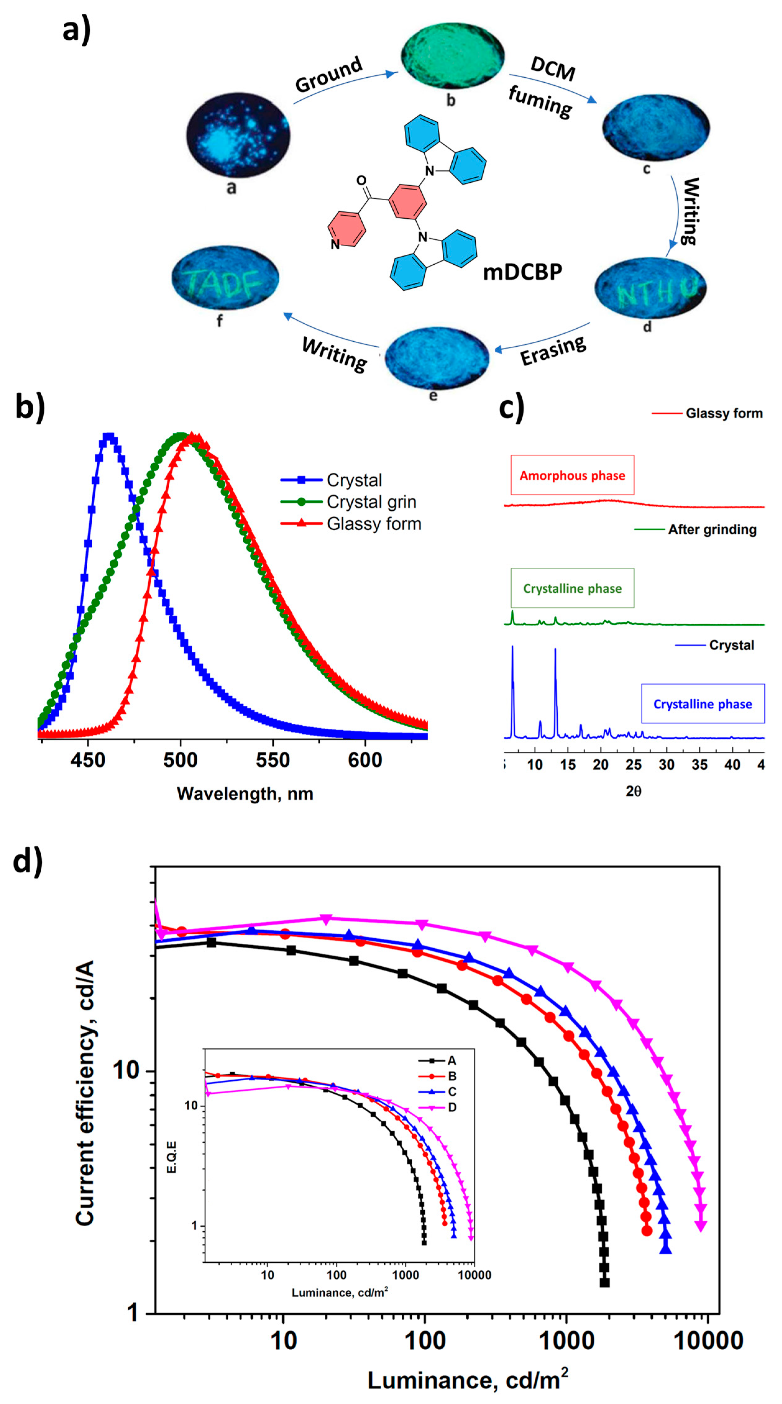
| OLED/mDCBP | 460/510 initial/well grinded | (0.16; 0.25) | 3.6 | 34.0 | 26.5 | 18.4 | 8900 | 0.2 | 0.06 | 474 | 90 | N/A | N/A | [112] |
| OLED/MeTPA-BQ | 650 | (0.64, 0.34) | 3.4 | 5.88 | 5.43 | 10.1 | N/A | 40.1 | 650 | 0.01 | 42 | 3.4 | 1.4 | [113] |
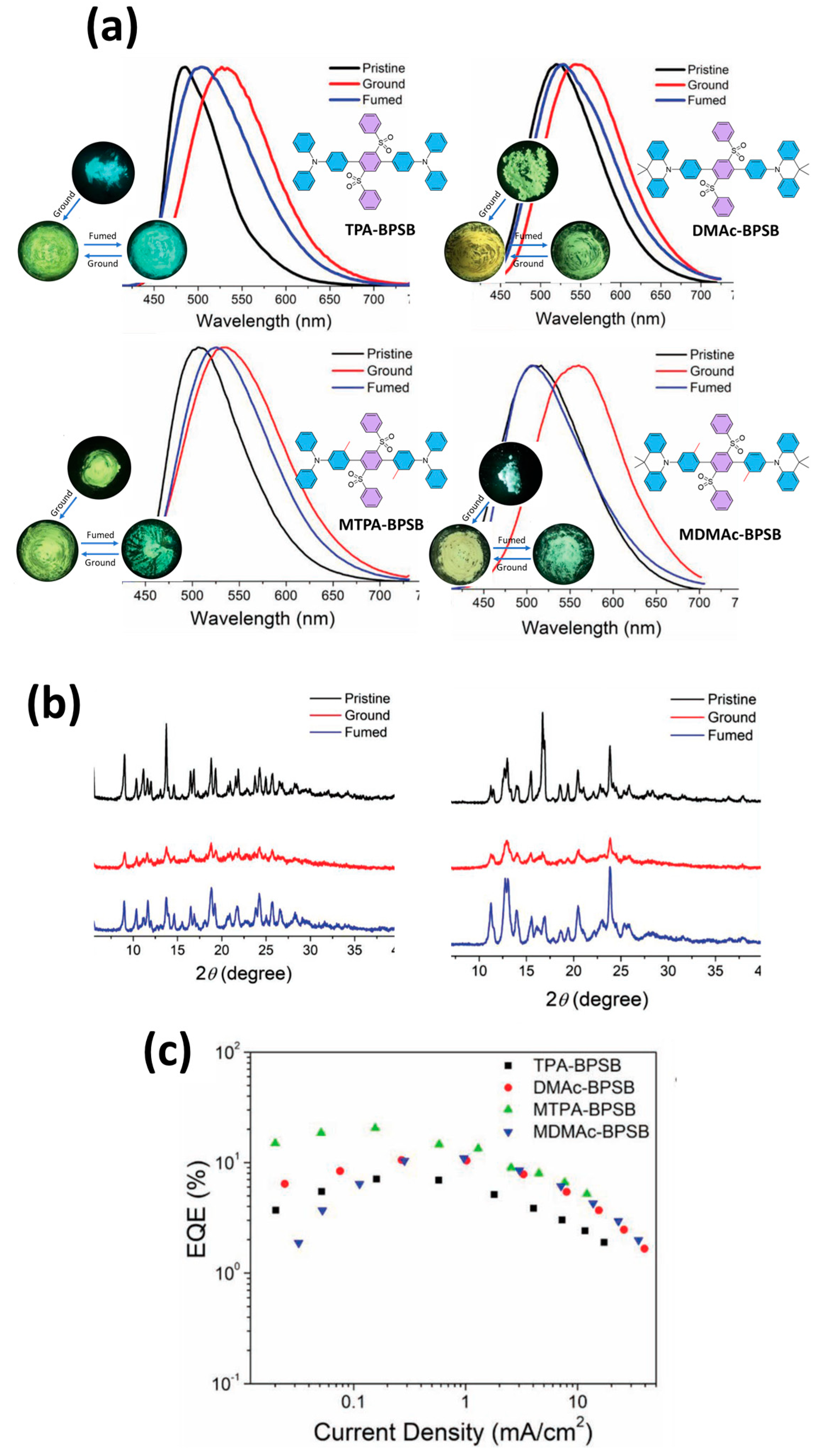
| OLED/MTPA-BPSB | 527 | (0.30, 0.50) | 3.2–4.8 | 61.6 | 37.2 | 20.5 | N/A | 10.6 | 0.07 | 527 | 76 | N/A | N/A | [114] |
| OLED/XT-BDPDBA | 486 | (0.158,0.341) | 3 | 55.0 | 57.5 | 27.0 | 19,319 | 2.4 | 0.025 | 484 | 91 | N/A | 22.0 | [115] |
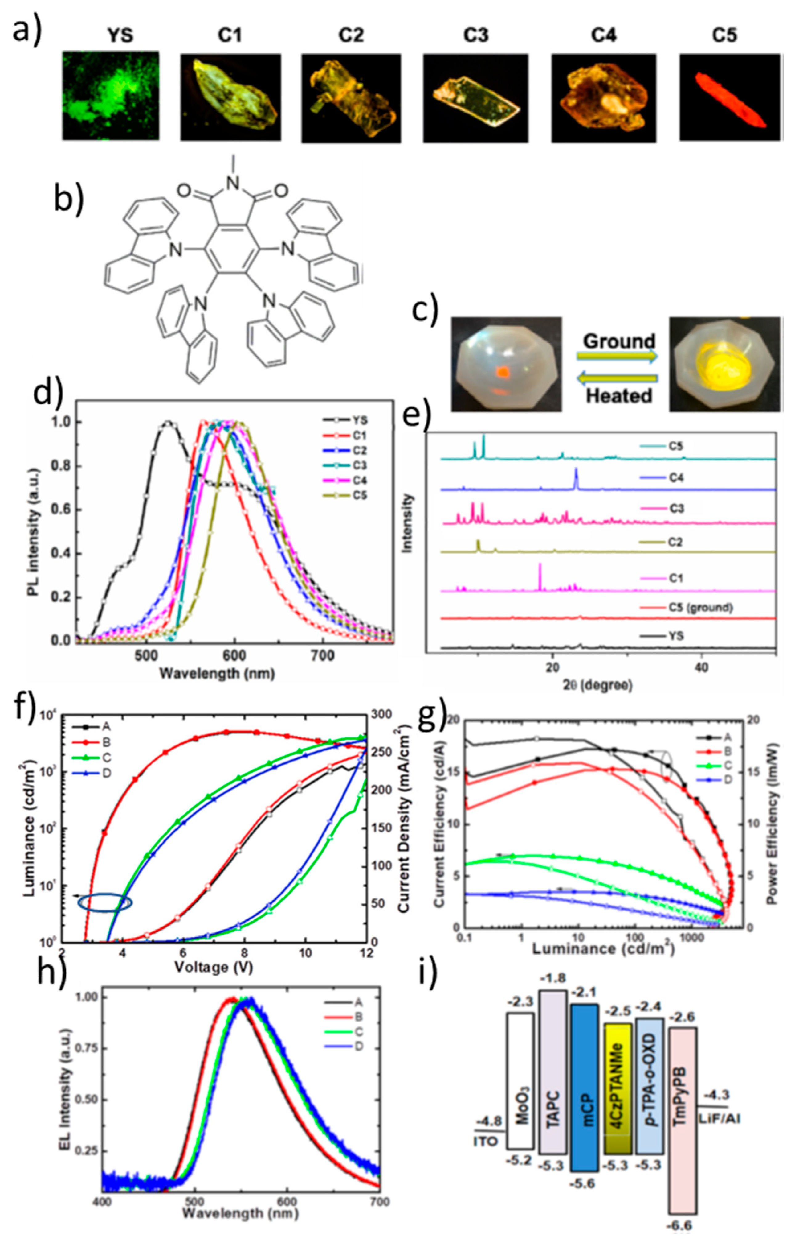
| OLED/4CzPTANMe | 602 | (0.59, 0.41) | 2.74 | 15.9 | 18.2 | 5.96 | N/A | 0.28 | 0.03 | 538 | 40 (ΦFL) | N/A | N/A | [116] |
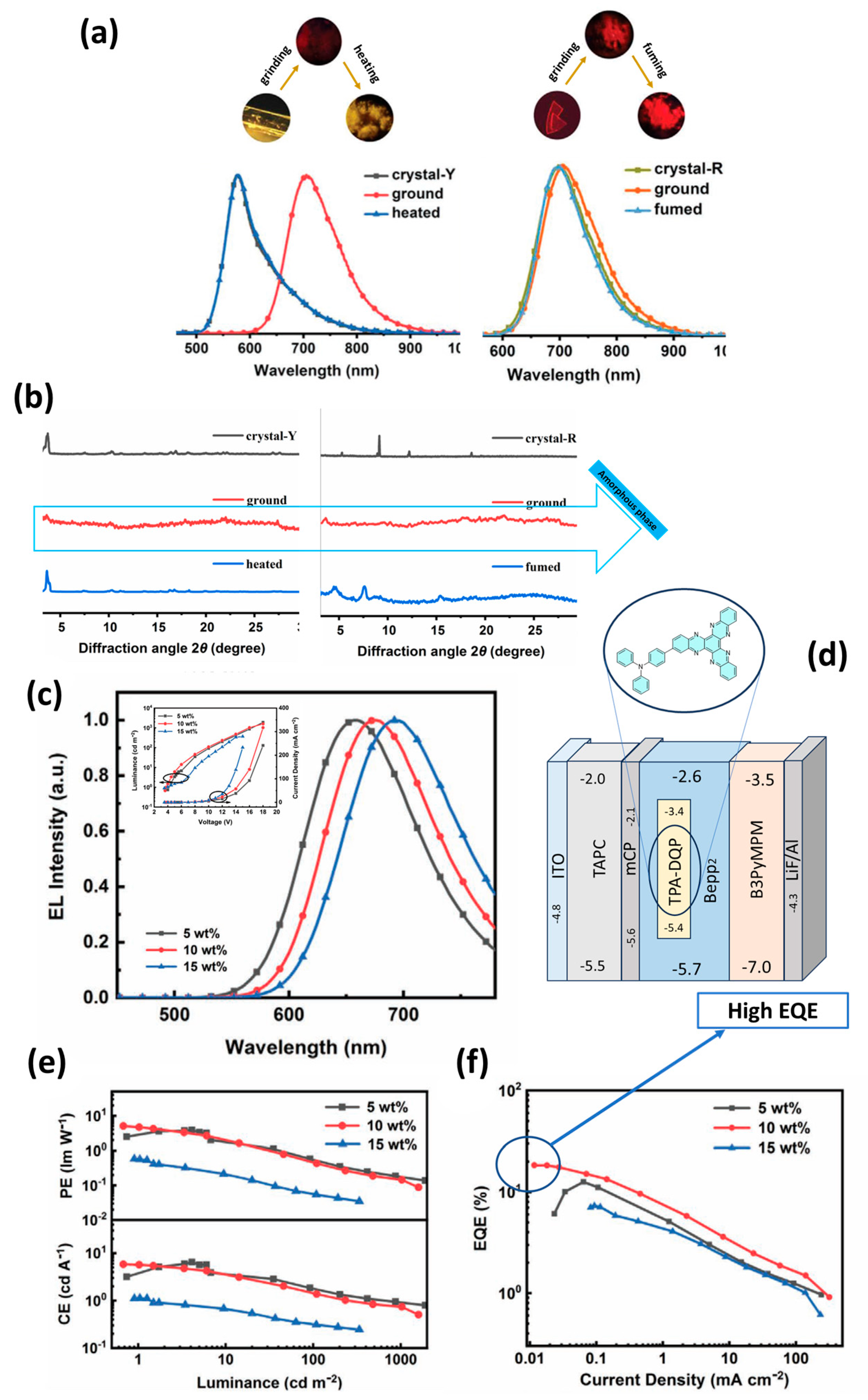
| OLED/TPA-DQP | 676 | (0.67, 0.32) | 3.8 | 5.69 | 4.7 | 18.3 | 1597 | 107.1 | 0.11 | 676 | 65 | N/A | N/A | [117] |
| LEC/fish-shaped structures based on carbazole derivatives | 520 | (0.344, 0.590) | 8.72 | 21.10 | 13.46 | 7.13 | 5944 | 6.8 | 0.04 | 533 | 39 | N/A | N/A | [118] |
Disclaimer/Publisher’s Note: The statements, opinions and data contained in all publications are solely those of the individual author(s) and contributor(s) and not of MDPI and/or the editor(s). MDPI and/or the editor(s) disclaim responsibility for any injury to people or property resulting from any ideas, methods, instructions or products referred to in the content. |
© 2025 by the authors. Licensee MDPI, Basel, Switzerland. This article is an open access article distributed under the terms and conditions of the Creative Commons Attribution (CC BY) license (https://creativecommons.org/licenses/by/4.0/).
Share and Cite
Ghahary, R.; Rabiei, M.; Nasiri, S.; Padgurskas, J.; Rukuiza, R. Overview on the Thermally Activated Delayed Fluorescence and Mechanochromic Materials: Bridging Efficiency and Versatility in LECs and OLEDs. Materials 2025, 18, 2714. https://doi.org/10.3390/ma18122714
Ghahary R, Rabiei M, Nasiri S, Padgurskas J, Rukuiza R. Overview on the Thermally Activated Delayed Fluorescence and Mechanochromic Materials: Bridging Efficiency and Versatility in LECs and OLEDs. Materials. 2025; 18(12):2714. https://doi.org/10.3390/ma18122714
Chicago/Turabian StyleGhahary, Raheleh, Marzieh Rabiei, Sohrab Nasiri, Juozas Padgurskas, and Raimundas Rukuiza. 2025. "Overview on the Thermally Activated Delayed Fluorescence and Mechanochromic Materials: Bridging Efficiency and Versatility in LECs and OLEDs" Materials 18, no. 12: 2714. https://doi.org/10.3390/ma18122714
APA StyleGhahary, R., Rabiei, M., Nasiri, S., Padgurskas, J., & Rukuiza, R. (2025). Overview on the Thermally Activated Delayed Fluorescence and Mechanochromic Materials: Bridging Efficiency and Versatility in LECs and OLEDs. Materials, 18(12), 2714. https://doi.org/10.3390/ma18122714