
Fs Laser Patterning of Amorphous As2S3 Thin Films


 ,
,  , , and
Abstract
1. Introduction
2. Materials and Methods
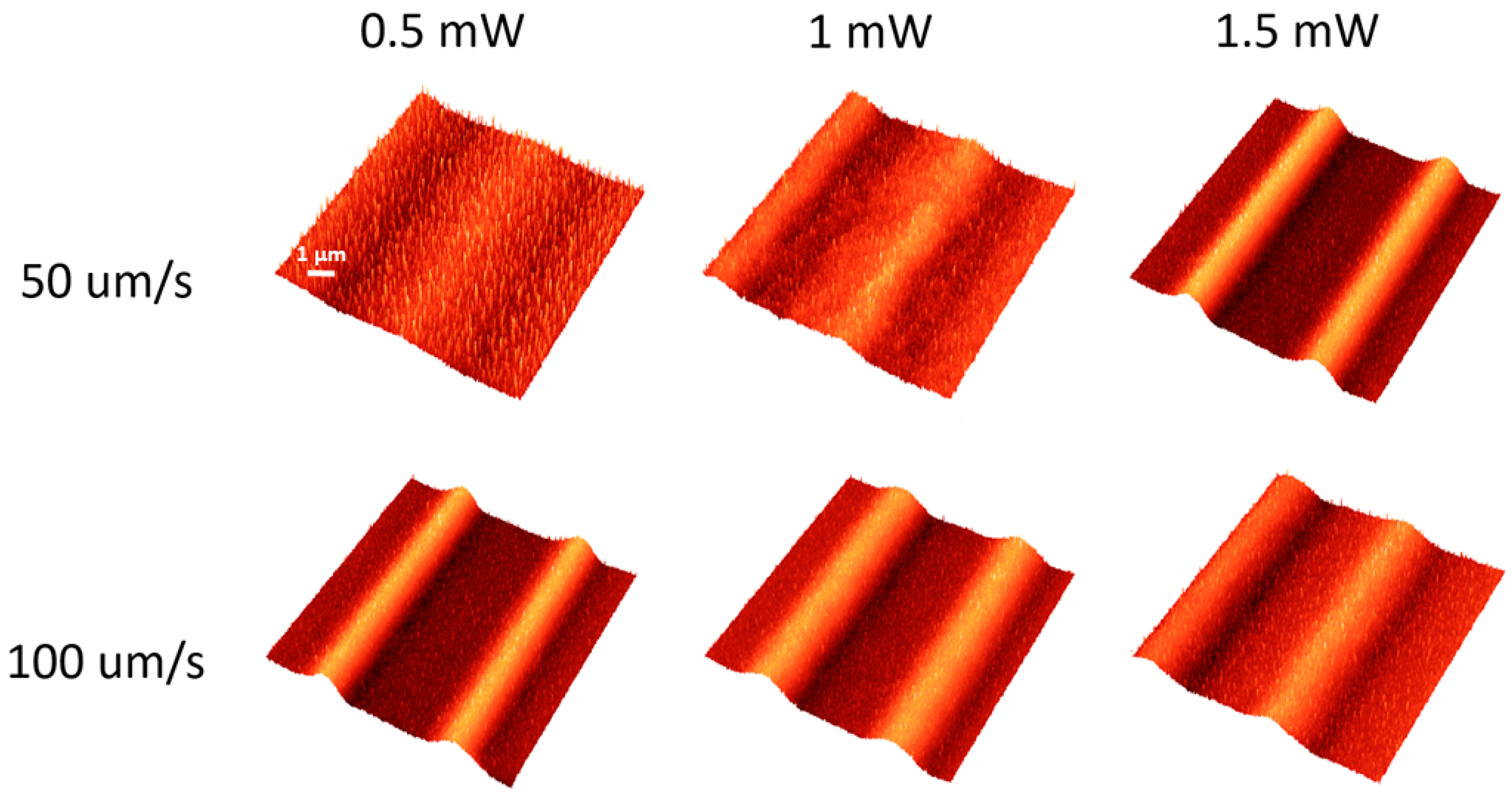
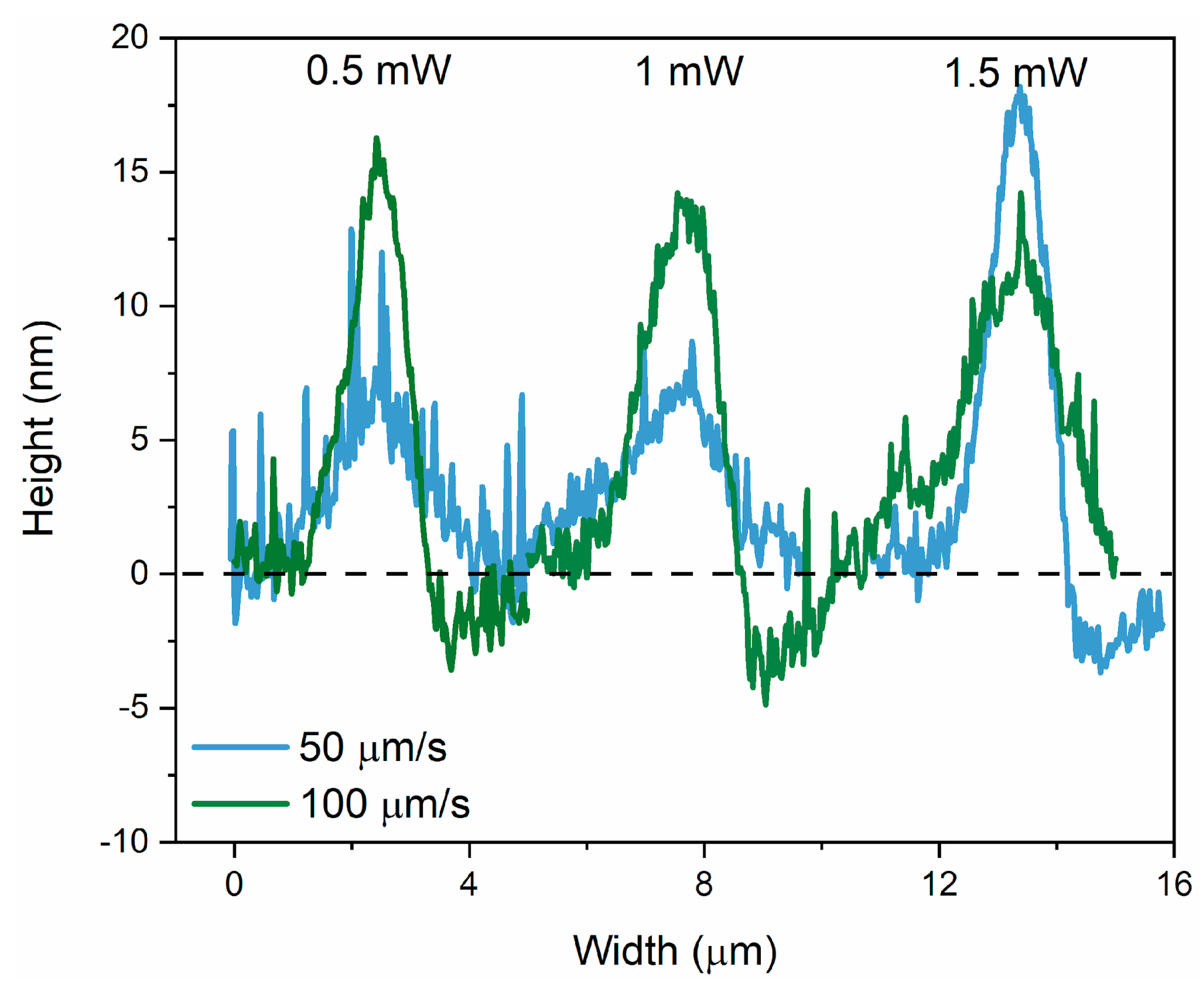
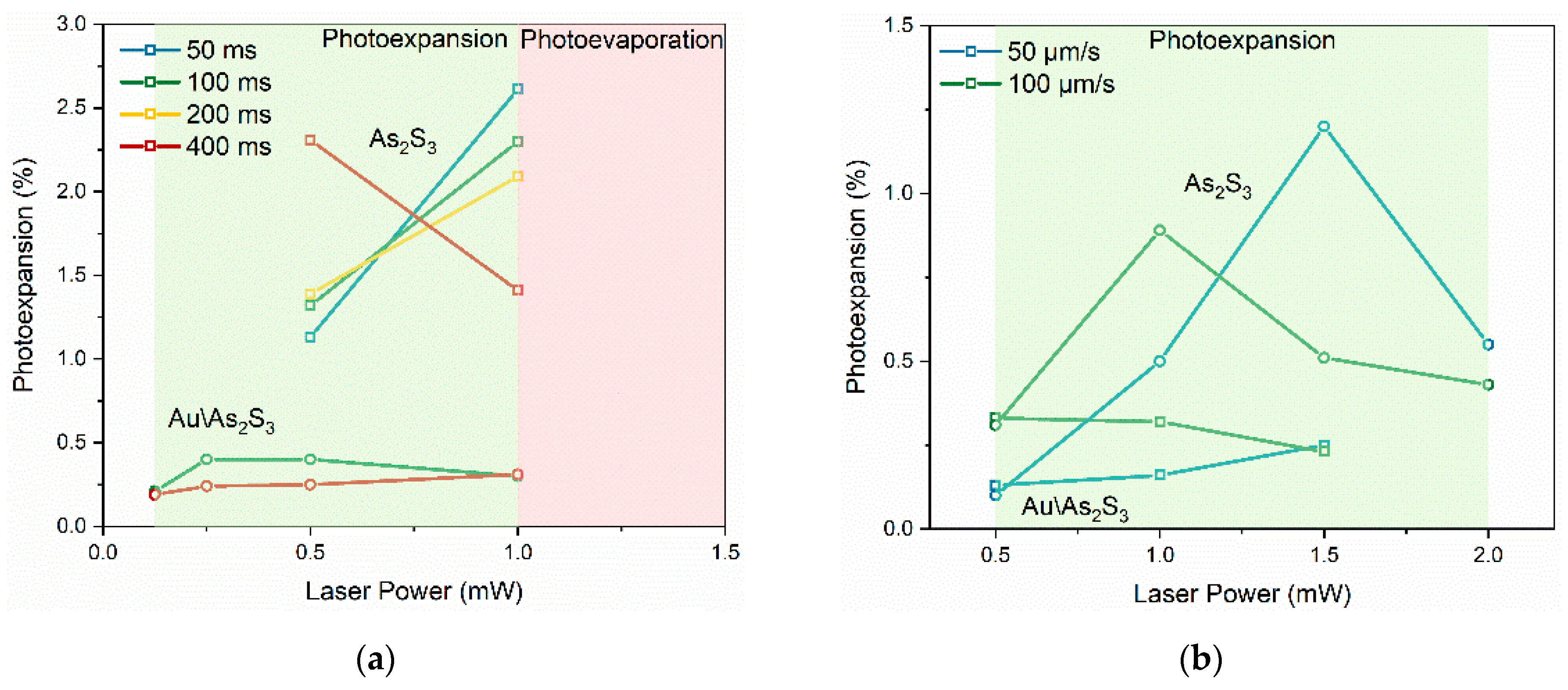
3. Results and Discussion
4. Conclusions
Author Contributions
Funding
Institutional Review Board Statement
Informed Consent Statement
Data Availability Statement
Conflicts of Interest
References
- Kolobov, A.V.; Kuznetsov, V.G.; Krbal, M.; Zabotnov, S.V. Lone-Pair-Enabled Polymorphism and Photostructural Changes in Chalcogenide Glasses. Materials 2023, 16, 6602. [Google Scholar] [CrossRef]
- Bureau, B.; Maurugeon, S.; Charpentier, F.; Adam, J.-L.; Boussard-Plédel, C.; Zhang, X.-H. Chalcogenide Glass Fibers for Infrared Sensing and Space Optics. Fiber Integr. Opt. 2009, 28, 65–80. [Google Scholar] [CrossRef]
- Zhang, X.; Guimond, Y.; Bellec, Y. Production of complex chalcogenide glass optics by molding for thermal imaging. J. Non-Cryst. Solids 2003, 326–327, 519–523. [Google Scholar] [CrossRef]
- Mägi, E.C.; Fu, L.B.; Nguyen, H.C.; Lamont, M.R.E.; Yeom, D.I.; Eggleton, B.J. Enhanced Kerr nonlinearity in sub-wavelength diameter As2Se3 chalcogenide fiber tapers. Opt. Express 2007, 15, 10324–10329. [Google Scholar] [CrossRef]
- Anderson, T.; Petit, L.; Carlie, N.; Choi, J.; Hu, J.; Agarwal, A.; Kimerling, L.; Richardson, K.; Richardson, M. Femtosecond laser photo-response of Ge23Sb7S70 films. Opt. Express 2008, 16, 20081–20098. [Google Scholar] [CrossRef]
- Li, L.; Lin, H.; Qiao, S.; Zou, Y.; Danto, S.; Richardson, K.; Musgraves, J.D.; Lu, N.; Hu, J. Integrated flexible chalcogenide glass photonic devices. Nat. Photonics 2014, 8, 643–649. [Google Scholar] [CrossRef]
- Shuleiko, D.; Zabotnov, S.; Sokolovskaya, O.; Poliakov, M.; Volkova, L.; Kunkel, T.; Kuzmin, E.; Danilov, P.; Kudryashov, S.; Pepelayev, D.; et al. Hierarchical Surface Structures and Large-Area Nanoscale Gratings in As2S3 and As2Se3 Films Irradiated with Femtosecond Laser Pulses. Materials 2023, 16, 4524. [Google Scholar] [CrossRef] [PubMed]
- Adam, J.; Calvez, L.; Trolès, J.; Nazabal, V. Chalcogenide Glasses for Infrared Photonics. Int. J. Appl. Glas. Sci. 2015, 6, 287–294. [Google Scholar] [CrossRef]
- Zhang, Q.; Lin, H.; Jia, B.; Xu, L.; Gu, M. Nanogratings and nanoholes fabricated by direct femtosecond laser writing in chalcogenide glasses. Opt. Express 2010, 18, 6885–6890. [Google Scholar] [CrossRef]
- Seong, D.; Lee, S.Y.; Seo, H.K.; Kim, J.-W.; Park, M.; Yang, M.K. Highly Reliable Ovonic Threshold Switch with TiN/GeTe/TiN Structure. Materials 2023, 16, 2066. [Google Scholar] [CrossRef]
- Raeis-Hosseini, N.; Rho, J. Metasurfaces Based on Phase-Change Material as a Reconfigurable Platform for Multifunctional Devices. Materials 2017, 10, 1046. [Google Scholar] [CrossRef]
- Adam, J.L.; Zhang, X. (Eds.) Chalcogenide Glasses: Preparation, Properties and Applications; Woodhead Pub: Philadelphia, PA, USA, 2013. [Google Scholar]
- Bindra, K.S.; Bookey, H.T.; Kar, A.K.; Wherrett, B.S.; Liu, X.; Jha, A. Nonlinear optical properties of chalcogenide glasses: Observation of multiphoton absorption. Appl. Phys. Lett. 2001, 79, 1939–1941. [Google Scholar] [CrossRef]
- Fazio, E.; Hulin, D.; Chumash, V.; Michelotti, F.; Andriesh, A.; Bertolotti, M. On-off resonance femtosecond non-linear absorption of chalcogenide glassy films. J. Non-Cryst. Solids 1994, 168, 213–222. [Google Scholar] [CrossRef]
- Popescu, A.; Miclos, S.; Savastru, D.; Savastru, R.; Ciobanu, M.; Popescu, M.; Lorinczi, A.; Sava, F.; Velea, A.; Jipa, F.; et al. Direct laser writing of two-dimensional photonic structures in amorphous As2S3 thin films. J. Optoelectron. Adv. M. 2009, 11, 1874–1880. [Google Scholar]
- Velea, A.; Popescu, M.; Sava, F.; Lőrinczi, A.; Simandan, I.D.; Socol, G.; Mihailescu, I.N.; Stefan, N.; Jipa, F.; Zamfirescu, M.; et al. Photoexpansion and nano-lenslet formation in amorphous As2S3 thin films by 800 nm femtosecond laser irradiation. J. Appl. Phys. 2012, 112, 033105. [Google Scholar] [CrossRef]
- Torun, G.; Kishi, T.; Bellouard, Y. Direct-write laser-induced self-organization and metallization beyond the focal volume in tellurite glass. Phys. Rev. Mater. 2021, 5, 055201. [Google Scholar] [CrossRef]
- Fernandez, T.; Sakakura, M.; Eaton, S.; Sotillo, B.; Siegel, J.; Solis, J.; Shimotsuma, Y.; Miura, K. Bespoke photonic devices using ultrafast laser driven ion migration in glasses. Prog. Mater. Sci. 2017, 94, 68–113. [Google Scholar] [CrossRef]
- Musgraves, J.D.; Carlie, N.; Petit, L.; Boudebs, G.; Choi, J.; Richardson, M.; Richardson, K. Effect of Replacement of As by Ge and Sb on the Photo-Response under Near Infrared Femtosecond Laser Irradiation in As-based Sulfide Glasses. Int. J. Appl. Glas. Sci. 2011, 2, 308–320. [Google Scholar] [CrossRef]
- Hu, Y.; Tian, K.; Li, T.; Zhang, M.; Ren, H.; Qi, S.; Yang, A.; Feng, X.; Yang, Z. Mid-infrared nonlinear optical performances of Ge-Sb-S chalcogenide glasses. Opt. Mater. Express 2021, 11, 695–706. [Google Scholar] [CrossRef]
- Feltz, A.; Burckhardt, W.; Voigt, B.; Linke, D. Optical glasses for IR transmittance. J. Non-Cryst. Solids 1991, 129, 31–39. [Google Scholar] [CrossRef]
- Popescu, M.; Velea, A.; Lorinczi, A.; Zamfirescu, M.; Jipa, F.; Miclos, S.; Popescu, A.; Ciobanu, M.; Savastru, D. Two dimensional photonic structures based on As-S chalcogenide glass. Dig. J. Nanomater. Bios. 2010, 5, 1101–1105. [Google Scholar]
- Paula, K.T.; Dutta, N.S.; Almeida, J.M.; Nolasco, L.; Andrade, M.B.; Arnold, C.B.; Mendonça, C.R. Femtosecond laser induced damage threshold incubation and oxidation in AS2S3 and AS2Se3 thin films. Appl. Surf. Sci. 2024, 654, 159449. [Google Scholar] [CrossRef]
- Kang, M.; Triplett, B.M.; Shalaginov, M.Y.; Deckoff-Jones, S.; Blanco, C.; Truman, M.; Shirshneva-Vashchenko, E.; Cook, J.; Du, Q.; Karnik, T.S.; et al. Photochemically Engineered Large-Area Arsenic Sulfide Micro-Gratings for Hybrid Diffractive–Refractive Infrared Platforms. Adv. Photon-Res. 2024, 5, 2300241. [Google Scholar] [CrossRef]
- Verger, F.; Pain, T.; Nazabal, V.; Boussard-Plédel, C.; Bureau, B.; Colas, F.; Rinnert, E.; Boukerma, K.; Compère, C.; Guilloux-Viry, M.; et al. Surface enhanced infrared absorption (SEIRA) spectroscopy using gold nanoparticles on As2S3 glass. Sens. Actuators B Chem. 2012, 175, 142–148. [Google Scholar] [CrossRef]
- Tanaka, K. Have we understood the optical absorption edge in chalcogenide glasses? J. Non-Cryst. Solids 2016, 431, 21–24. [Google Scholar] [CrossRef]
- Tanaka, K.; Shimakawa, K. Amorphous Chalcogenide Semiconductors and Related Materials, 2nd ed.; Springer: Cham, Switzerland, 2021. [Google Scholar]
- Hisakuni, H.; Tanaka, K. Giant photoexpansion in As2S3 glass. Appl. Phys. Lett. 1994, 65, 2925–2927. [Google Scholar] [CrossRef]
- Tanaka, K. Spectral dependence of photoexpansion in As2S3 glass. Philos. Mag. Lett. 1999, 79, 25–30. [Google Scholar] [CrossRef]
- Wang, H.; Qi, D.; Yu, X.; Zhang, Y.; Zhang, Z.; Xu, T.; Zhang, X.; Dai, S.; Shen, X.; Song, B.; et al. In-Situ and Ex-Situ Characterization of Femtosecond Laser-Induced Ablation on As2S3 Chalcogenide Glasses and Advanced Grating Structures Fabrication. Materials 2018, 12, 72. [Google Scholar] [CrossRef]
- Csarnovics, I.; Veres, M.; Nemec, P.; Molnár, S.; Kökényesi, S. Surface plasmon enhanced light-induced changes in Ge-Se amorphous chalcogenide—Gold nanostructures. J. Non-Cryst. Solids 2021, 553, 120491. [Google Scholar] [CrossRef]
- Jain, H.; Vlcek, M. Glasses for lithography. J. Non-Cryst. Solids 2008, 354, 1401–1406. [Google Scholar] [CrossRef]
- Kovalskiy, A.; Cech, J.; Vlcek, M.; Waits, C.M.; Dubey, M.; Heffner, W.R.; Jain, H. Chalcogenide glass e-beam and photoresists for ultrathin grayscale patterning. J. Micro/Nanolithography MEMS MOEMS 2009, 8, 043012. [Google Scholar] [CrossRef]
- Sava, F.; Popescu, M.; Lőrinczi, A.; Velea, A. Possible mechanism of Ag photodiffusion in a-As2S3 thin films. Phys. Status Solidi (B) 2013, 250, 999–1003. [Google Scholar] [CrossRef]
- Charnovych, S.; Kokenyesi, S.; Glodán, G.; Csik, A. Enhancement of photoinduced transformations in amorphous chalcogenide film via surface plasmon resonances. Thin Solid Film. 2011, 519, 4309–4312. [Google Scholar] [CrossRef]
- Lyubin, V.; Klebanov, M.; Rosenwaks, S.; Volterra, V. Anisotropy of photoinduced light-scattering in glassy As2S3. J. Non-Cryst. Solids 1993, 164–166, 1165–1168. [Google Scholar] [CrossRef]
- Kolobov, A.V.; Lyubin, V.; Yasuda, T.; Klebanov, M.; Tanaka, K. Photoinduced anisotropy in vitreousAs2S3:mA reflectance-difference study. Phys. Rev. B 1997, 55, 8788–8792. [Google Scholar] [CrossRef]
- Morigaki, K. Physics of Amorphous Semiconductors; Imperial College Press: London, UK, 1999. [Google Scholar]
- Tanaka, K. The charged defect exists? J. Optoelectron. Adv. Mater. 2001, 3, 189–198. [Google Scholar]
- Juodkazis, S.; Kondo, T.; Misawa, H.; Rode, A.; Samoc, M.; Luther-Davies, B. Photo-structuring of As2S3glass by femtosecond irradiation. Opt. Express 2006, 14, 7751–7756. [Google Scholar] [CrossRef]
- Hisakuni, H.; Tanaka, K. Optical Microfabrication of Chalcogenide Glasses. Science 1995, 270, 974–975. [Google Scholar] [CrossRef]
- Popescu, M.; Lőrinczi, A.; Sava, F.; Velea, A.; Simandan, I.; Badica, P.; Burdusel, M.; Galca, A.; Socol, G.; Jipa, F.; et al. Thin films of amorphous Ga2S3 and rare-earth sulphides. Mater. Lett. 2015, 142, 229–231. [Google Scholar] [CrossRef]
- Lőrinczi, A.; Sava, F.; Simandan, I.-D.; Velea, A.; Popescu, M. Photoexpansion in amorphous As2S3: A new explanation. J. Non-Cryst. Solids 2016, 447, 123–125. [Google Scholar] [CrossRef]
- Popescu, M.; Velea, A.; Miclos, S.; Savastru, D. Optics of microlenses created by irradiation of As2S3amorphous chalcogenide films with femtosecond laser pulses. Philos. Mag. Lett. 2013, 93, 213–220. [Google Scholar] [CrossRef]
- Moreno, T.V.; Zanuto, V.S.; Astrath, N.G.; Silva, G.R.; Fonseca, E.J.; Souza, S.T.; Zhao, D.; Jain, H.; Malacarne, L.C. In situ measurements of photoexpansion inAs2S3bulk glass by atomic force microscopy. Opt. Mater. 2019, 94, 9–14. [Google Scholar] [CrossRef]
- Tanaka, K.; Saitoh, A. Pulsed light effects in amorphous As2S3: Review. J. Mater. Sci. Mater. Electron. 2022, 33, 22029–22052. [Google Scholar] [CrossRef]
- Zhao, D.; Jain, H.; Malacarne, L.C.; Pedreira, P.R.B. Role of photothermal effect in photoexpansion of chalcogenide glasses. Phys. Status Solidi (B) 2013, 250, 983–987. [Google Scholar] [CrossRef]
- Fritzsche, H. Photo-induced fluidity of chalcogenide glasses. Solid State Commun. 1996, 99, 153–155. [Google Scholar] [CrossRef]


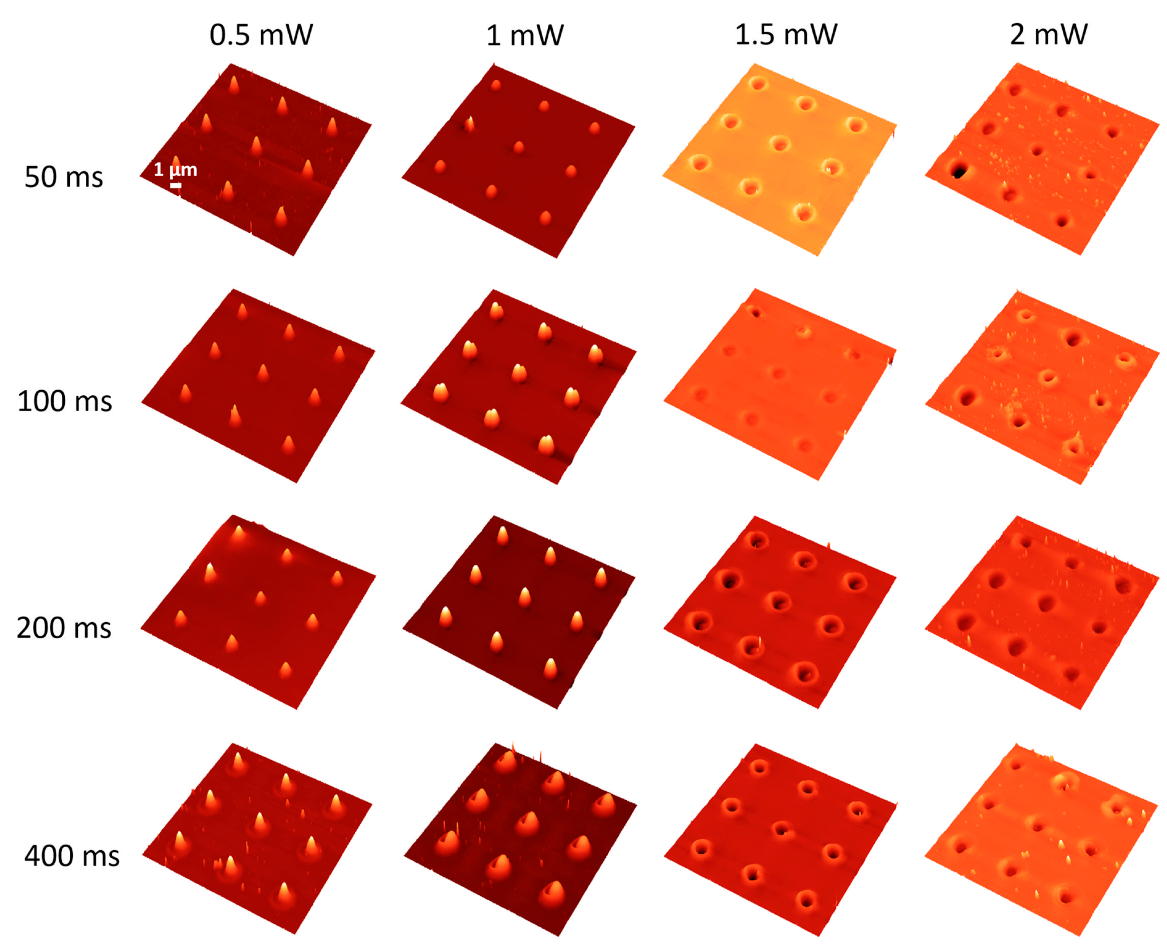
| Average Laser Power (mW) | 0.5 | 1 | 1.5 | 2 | |
|---|---|---|---|---|---|
| Laser Fluence (µJ/cm2) | 88.5 | 176.9 | 265.4 | 353.9 | |
| Laser Intensity (MW/cm2) | 5.9 | 11.8 | 17.7 | 23.6 | |
| Exposure Time | Computed Parameter | ||||
| 50 ms | A (µm2) | 0.034 | 0.097 | 0.043 | 0.092 |
| w (µm) | 0.51 | 0.63 | 0.72 | 0.56 | |
| (%) | 2.3 | 5.2 | - | - | |
| h/d (nm) | 52 | 112 | 44 | 119 | |
| 100 ms | A (µm2) | 0.039 | 0.084 | 0.038 | 0.111 |
| w (µm) | 0.50 | 0.62 | 0.73 | 0.63 | |
| (%) | 5.2 | 4.6 | - | - | |
| h/d (nm) | 62 | 103 | 46 | 133 | |
| 200 ms | A (µm2) | 0.046 | 0.080 | 0.026 | 0.097 |
| w (µm) | 0.56 | 0.65 | 0.80 | 0.72 | |
| (%) | 2.8 | 4.2 | - | - | |
| h/d (nm) | 63 | 91 | 25 | 98 | |
| 400 ms | A (µm2) | 0.071 | 0.064 | 0.039 | 0.099 |
| w (µm) | 0.52 | 0.77 | 0.50 | 0.74 | |
| (%) | 4.6 | 2.8 | - | - | |
| h/d (nm) | 110 | 66 | 49 | 99 | |
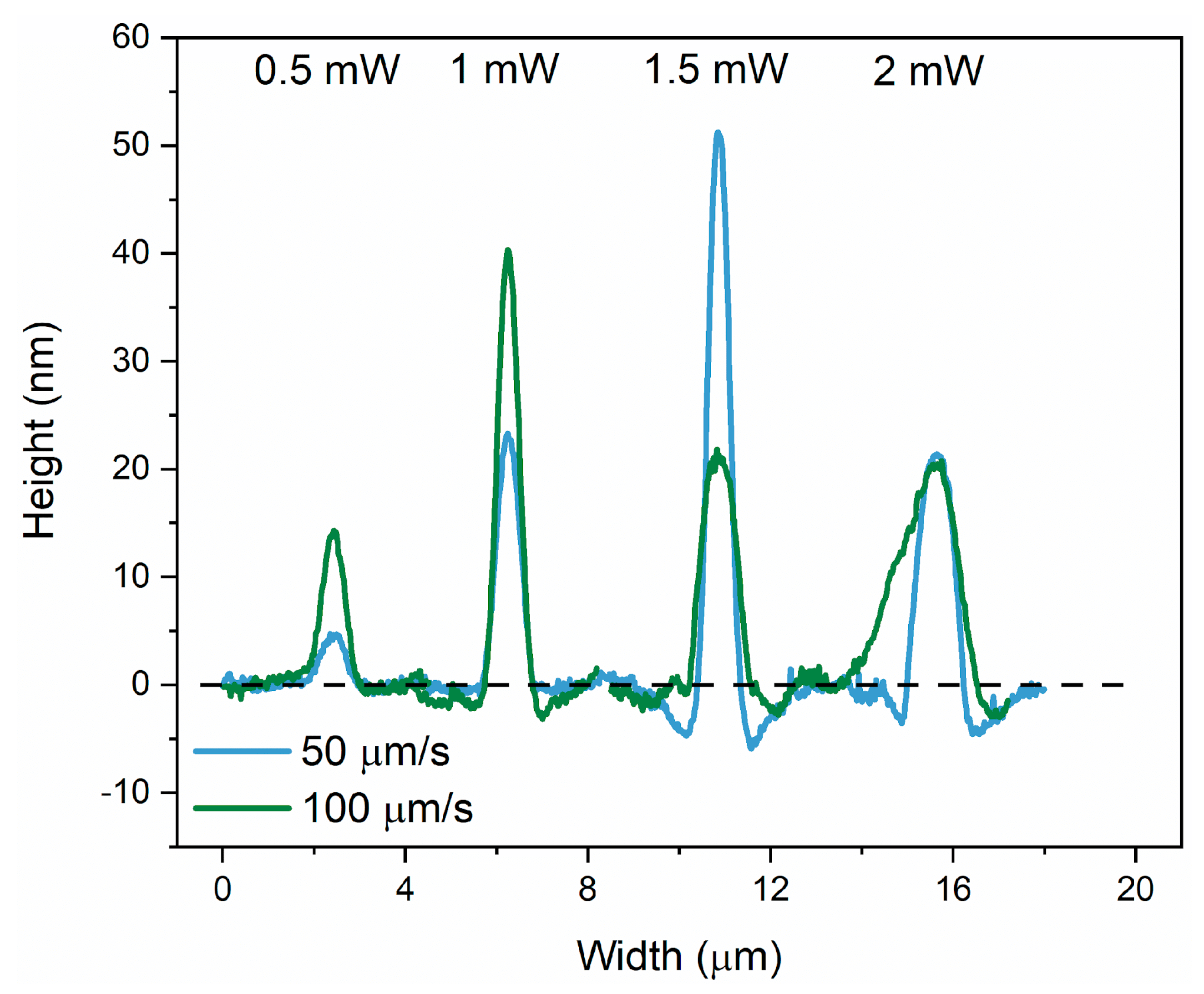
| CW Laser Power (mW) | 0.5 | 1 | 1.5 | 2 | |
|---|---|---|---|---|---|
| Laser Intensity (kW/cm2) | 7.1 | 14.2 | 21.2 | 28.3 | |
| Laser Scanning Speed | Computed Parameter | ||||
| 50 µm/s | A (µm2) | 0.003 | 0.014 | 0.029 | 0.021 |
| w (µm) | 0.50 | 0.47 | 0.41 | 0.65 | |
| (%) | 0.2 | 1.0 | 2.4 | 1.1 | |
| h (nm) | 5 | 23 | 51 | 22 | |
| 100 µm/s | A (µm2) | 0.009 | 0.023 | 0.021 | 0.032 |
| w (µm) | 0.49 | 0.44 | 0.70 | 1.24 | |
| (%) | 0.6 | 1.8 | 1.0 | 0.9 | |
| h (nm) | 15 | 40 | 23 | 22 | |
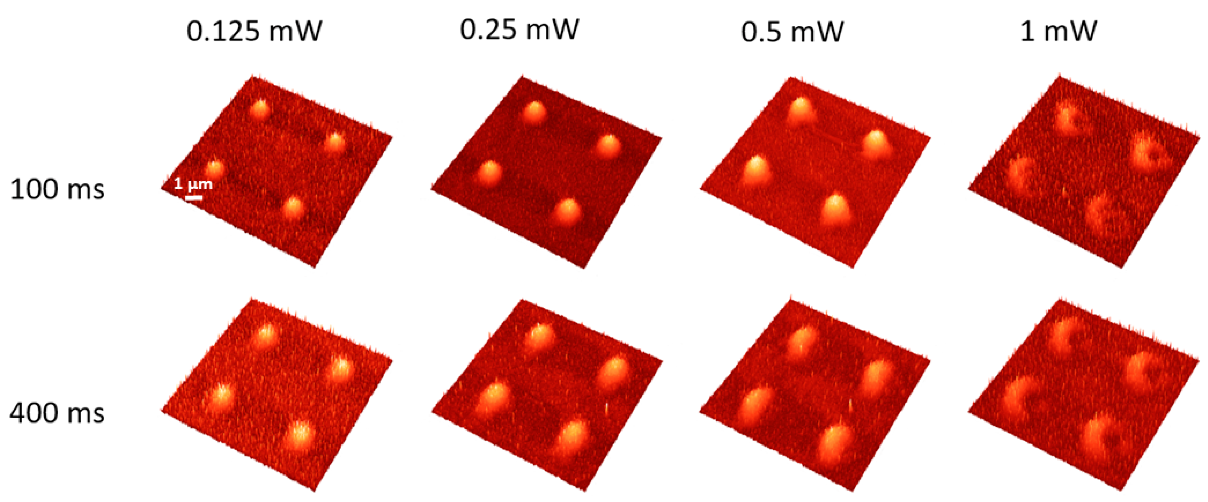
| Average Laser Power (mW) | 0.125 | 0.25 | 0.5 | 1 | |
|---|---|---|---|---|---|
| Laser Fluence (µJ/cm2) | 22.125 | 44.25 | 88.5 | 176.9 | |
| Laser Intensity (MW/cm2) | 1.475 | 2.95 | 5.9 | 11.8 | |
| Exposure Time | Computed Parameter | ||||
| 100 ms | A (µm2) | 0.009 | 0.019 | 0.022 | 0.011 |
| w (µm) | 0.71 | 0.81 | 0.94 | 0.62 | |
| (%) | 0.4 | 0.8 | 0.8 | 0.6 | |
| h (nm) | 10 | 18 | 19 | 16 | |
| 400 ms | A (µm2) | 0.010 | 0.014 | 0.013 | 0.013 |
| w (µm) | 0.87 | 0.99 | 0.89 | 0.72 | |
| (%) | 0.4 | 0.5 | 0.5 | 0.6 | |
| h (nm) | 10 | 12 | 11 | 16 | |
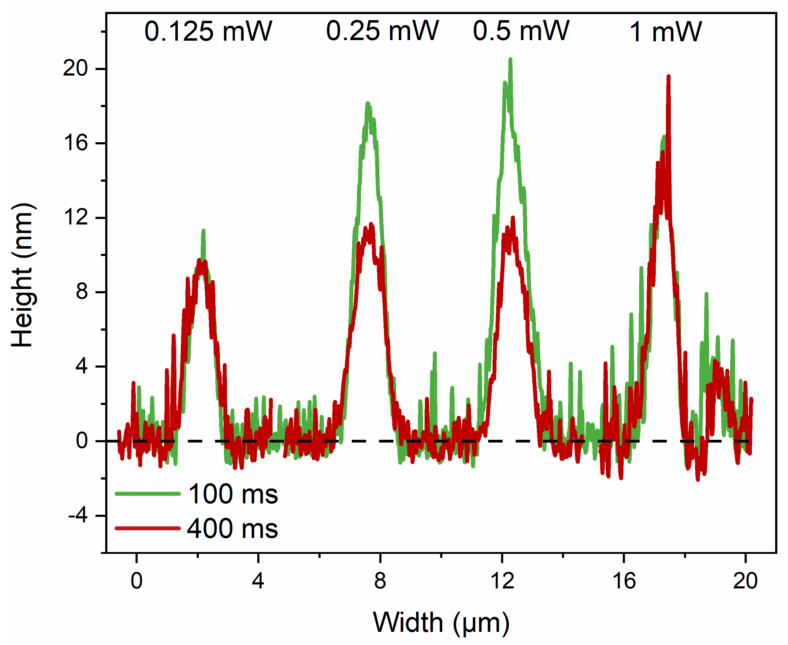
| CW Laser Power (mW) | 0.5 | 1 | 1.5 | |
|---|---|---|---|---|
| Laser Intensity (kW/cm2) | 7.1 | 14.2 | 21.2 | |
| Laser Scanning Speed | Computed Parameter | |||
| 50 µm/s | A (µm2) | 0.012 | 0.013 | 0.014 |
| w (µm) | 1.46 | 1.34 | 0.93 | |
| (%) | 0.3 | 0.3 | 0.5 | |
| h (nm) | 7 | 7 | 18 | |
| 100 µm/s | A (µm2) | 0.018 | 0.023 | 0.027 |
| w (µm) | 0.92 | 1.20 | 1.75 | |
| (%) | 0.7 | 0.6 | 0.5 | |
| h (nm) | 16 | 14 | 11 |
Disclaimer/Publisher’s Note: The statements, opinions and data contained in all publications are solely those of the individual author(s) and contributor(s) and not of MDPI and/or the editor(s). MDPI and/or the editor(s) disclaim responsibility for any injury to people or property resulting from any ideas, methods, instructions or products referred to in the content. |
© 2024 by the authors. Licensee MDPI, Basel, Switzerland. This article is an open access article distributed under the terms and conditions of the Creative Commons Attribution (CC BY) license (https://creativecommons.org/licenses/by/4.0/).
Share and Cite
Mihai, C.; Jipa, F.; Socol, G.; Kiss, A.E.; Zamfirescu, M.; Velea, A. Fs Laser Patterning of Amorphous As2S3 Thin Films. Materials 2024, 17, 798. https://doi.org/10.3390/ma17040798
Mihai C, Jipa F, Socol G, Kiss AE, Zamfirescu M, Velea A. Fs Laser Patterning of Amorphous As2S3 Thin Films. Materials. 2024; 17(4):798. https://doi.org/10.3390/ma17040798
Chicago/Turabian StyleMihai, Claudia, Florin Jipa, Gabriel Socol, Adrian E. Kiss, Marian Zamfirescu, and Alin Velea. 2024. "Fs Laser Patterning of Amorphous As2S3 Thin Films" Materials 17, no. 4: 798. https://doi.org/10.3390/ma17040798
APA StyleMihai, C., Jipa, F., Socol, G., Kiss, A. E., Zamfirescu, M., & Velea, A. (2024). Fs Laser Patterning of Amorphous As2S3 Thin Films. Materials, 17(4), 798. https://doi.org/10.3390/ma17040798